Characterisation and
Performance
Optimisation of GaN
HEMTs and Amplifiers for
Radar Applications
Francesco Fornetti
A dissertation submitted to the University of Bristol in accordance with the requirements for award of the degree of Doctor of Philosophy in the Faculty of Engineering
Department of Electrical and Electronic Engineering December 2010
II
Abstract
New bandgap semiconductor materials, such as Gallium Nitride (GaN), promise to revolutionise the world of microwave power amplifiers by providing high power density, linear operation and robustness up to Ka-band frequencies (35GHz). Applications which require very high RF powers still utilise vacuum tube devices, thus a breakthrough in semiconductor technology is long overdue. Nevertheless, despite the great potential of these new technologies, they still suffer from physical and fabrication issues which may prevent devices fabricated on GaN and other III-V alloys from achieving the performance and reliability levels required. In addition, some of these issues, such as trapping effects, may be exacerbated when the devices are operated in pulsed mode as is done in Radar systems. A number of studies have investigated both commercial and prototype GaN devices in Continuous Wave (CW) mode. This thesis addresses the suitability of such devices to pulsed applications and provides corrective experimental characterisation and recommendations.
In this thesis, a thorough analysis of physics, technology and research status of GaN High Electron Mobility Transistors (HEMTs) is first presented. Amplifiers built around GaN HEMTs supplied by leading device manufacturers Cree and Nitronex are subsequently subjected to extensive investigations both in the frequency and time domain. Such tests aim at verifying the presence of possible trapping effects and their effect on the performance of pulsed GaN amplifiers. New measures, as Spectral Asymmetry and spectrum-derived Pulse Width Variation, are also introduced which may be useful performance indicators for pulsed amplifiers and be of aid to device manufacturers and circuit designers. In addition, device level tests are also carried out on both Cree and Nitronex devices which investigate the presence of the trapping effects, and their influence on the operation of pulsed amplifiers, though a dedicated pulsed I-V characterisation.
From the rigorous studies conducted, it was found that significant trapping effects are present in commercially available devices and, more importantly, that they have much longer time constants (10s and 100s of seconds) than are encountered in other technologies such as GaAs (ms). An appropriate characterisation setup is therefore required, at device level, in order to obtain meaningful I-V characteristics. Operational parameters such as pulse repetition frequency and duty cycle were also found to affect the I-V characteristic of the devices and should therefore be taken into account when designing pulsed amplifiers.
It was also observed that the performance of pulsed amplifiers based on Cree devices did not appear to be greatly affected by trapping effects across a wide range of Pulse Repetition Frequencies (PRFs) and power levels. This demonstrates that such GaN devices may be suitable for Radar applications. Nevertheless, when the amplifiers were pushed to higher drive levels, a considerable increase in fall time was observed which was chiefly due to third order non-linearites and could be modelled by means of third order polynomials. In addition, the new performance measures introduced were found to be very useful in the selection of appropriate bias points for the transistor. An appropriate choice of bias was found to considerably improve the performance of a pulsed amplifier in terms of pulse symmetry, spectral symmetry and efficiency. The automated test rig devised by the author will also be suited to the characterisation of higher frequency amplifiers which have recently become available.
III
Acknowledgements
First and foremost I would like to thank Prof Mark Beach for offering this wonderful opportunity to me, establishing the liaisons with MBDA and procuring the funding for my Ph.D. I would also like to thank him for being very understanding and supportive particularly through the difficult times. I am also thankful to Dr Kevin Morris for being my supervisor and for being engaging in our meetings and discussions.
I would also like to thank Chris Carter and MBDA for their support and help and for the interest and admiration that they have shown for my work.
I am also very grateful to Dr Jim Rathmell of the University of Sydney who, with his partner Rose, went out of his way to look after me during my time in Australia. Not only did he give me the opportunity to greatly further my technical knowledge but he also ensured that I was fully integrated in the teaching and research community of Sydney and Macquarie Universities.
Mr Ken Stevens deserves a really special mention for his help and support on both a technical and personal level. His encouragement and technical know-how were key to the successful realisation of the test setups used for the experiments.
I am also very grateful to Prof McGeehan for his advice and encouragement and for his support and praise for the hard work that I put into my research.
I would also like to thank Andrew Wallace and AWR Corporation for granting a free license for their simulation tools, Cree Inc and Nitronex for supplying free samples and Marco Brunetti for his help with the graphics.
In addition there are no words to express my gratitude to my dearest friends Magnus and Roger who were always there for me through all the adversities that life challenged me with in the last four years. Without their help, encouragement and support I could not have achieved this.
IV
Author’s Declaration
I declare that the work in this dissertation was carried out in accordance with the requirements of the University's Regulations and Code of Practice for Research Degree Programmes and that it has not been submitted for any other academic award. Except where indicated by specific reference in the text, the work is the candidate's own work. Work done in collaboration with, or with the assistance of, others, is indicated as such. Any views expressed in the dissertation are those of the author.
V
Table of Contents
1 Introduction ... 1
1.1 Solid State Power Amplifiers and Radar Transmitters ... 1
1.2 Monopulse Radar ... 5
1.3 Key Objectives ... 8
1.4 Overview of the Research Work ... 8
1.5 Contributions Made ... 10
2 Physics of Semiconductors and Heterojunctions ... 12
2.1 Introduction ... 12
2.2 Semiconductor Materials and High Frequency Solid State Electronic Devices ... 13
2.4 BasicHeterostructurePhysics ... 19
2.5 Modulation Doping ... 24
2.6 Band Bending and Carrier Transport Parallel to Heterojunctions ... 26
2.7 2DEG Mobility and Electron Sheet Density ... 29
3 GaN HEMTs: Physics, Limitations, Research Status and Commercial availability ... 31
3.1 HEMTs: Structure and Characteristics ... 31
3.2 Spontaneous and Piezoelectric Polarization Effects in AlGaN/GaN Heterostructures ... 33
3.3 GaN HEMTs ... 36
3.4 Research in GaN HEMTs: an Overview ... 40
3.5 Surface States... 41
3.6 Buffer Traps ... 44
3.7 The Concept of Virtual Gate... 46
3.8 DC Characterisation of GaN HEMTs ... 48
3.9 Drain Current Transients ... 50
3.10 RF Performance Limitations in GaN Transistors ... 53
3.11 Models ... 56 3.12 Field Plates ... 58 3.13 DHFET ... 61 3.14 Reliability ... 63 3.15 Substrates ... 63 3.16 Important Developments ... 64
VI
3.17 Commercial Availability of GaN HEMTs ... 66
3.18 Conclusions ... 69
4 Design and Characterisation Techniques for pulsed GaN Amplifiers ... 70
4.1 Introduction ... 70
4.2 Amplifier Design and Characteristics ... 71
4.3 The Modulator ... 74
4.4 Automated Measurement Test Rig ... 78
4.4.1 Setup 1 – Time Domain Measurements with Fast Digital Scope ... 78
4.4.2 Setup 2 - Frequency Domain Measurements with Signal Analyser ... 80
4.4.3 Alternative Tests ... 83
4.5 Conclusions ... 83
5 Characterisation and Performance Evaluation of Pulsed GaN Amplifiers ... 85
5.1 Introduction ... 85
5.2 Time Domain Measurements ... 87
5.2.1 Preliminary Tests ... 87
5.2.2 Power and Gain Profiles ... 98
5.2.3 Switching Times ... 101
5.2.4 Time Waveforms ... 106
5.3 Frequency Domain Measurements ... 109
5.3.1 Power Profiles ... 109
5.3.2 Spectral power imbalance ... 109
5.3.3 Zero Span Time Domain Envelope Analysis ... 111
5.3.4 Pulse Width Deviation ... 113
5.4 Conclusions ... 115
6 Pulsed IV Characterisation of GaN HEMTs ... 118
6.1 Introduction ... 118
6.2 The APSPA System ... 119
6.3 Long Time Constant Traps ... 120
6.3.1 Nitronex NPTB00025 ... 120
6.3.2 Cree CGH40010 ... 122
6.4 Pseudo-DC Characteristics ... 124
6.4.1 Nitronex ... 124
6.4.2 Cree ... 127
VII
6.5.1 Nitronex ... 130
6.5.2 Cree ... 132
6.6 The Importance at Settling Time... 133
6.7 Current Vs Time ... 134
6.7.1 Nitronex ... 134
6.7.2 Cree ... 135
6.8 Conclusions ... 136
7 Conclusions and Future Work ... 138
7.1 Conclusions ... 138
7.2 Future Work ... 141
7.2.1 High Frequency Devices ... 142
7.2.2 High Frequency Time Domain Measurements ... 143
7.2.3 Extended Pulsed IV Characterisation ... 144
7.2.4 Noise in Inter-Pulse period ... 145
References ... 146
Appendix A ... 151
VIII
Abbreviations
2DEG 2 Dimensional Electron Gas 2DHG 2 Dimensional Hole GasC-Band 4-8 GHz
CFA Cross Field Amplifier
CW Continuous Wave
DARPA Defense Advanced Research Projects Agency DBI Digital Bandwidth Interleave
DHFET Double Heterojunction Field Effect Transistors
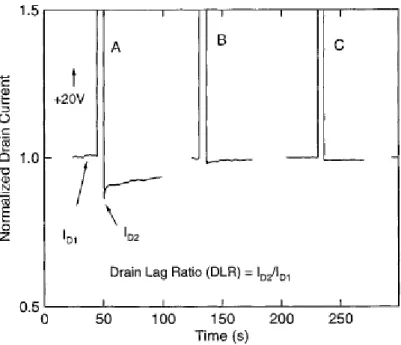
DLR Drain Lag Ratio
DMD Diamond Microwave Devices
FET Field Effect Transistor
FP Field Plate
GaAs Gallium Arsenide
GaN Gallium Nitride
GC-FP Gate Connected Field Plate HBT Heterojunction Bipolar Transistor HEMT High Electron Mobility Transistor Ka-Band 26.5-40 GHz
KTS Knowledge Transfer Secondment Ku-Band 12-18 GHz
L-Band 1-2 GHz
MBE Molecular Beam Epitaxy
MESFET Metal Semiconductor Field Effect Transistor MOCVD Metal-Organic Chemical Vapour Deposition MTBF Mean Time Between Failures
PAE Power Added Efficiency PRF Pulse Repetition Frequency
S-Band 2-4 GHz
SBH Schottky Barrier Height SC-FP Source Connected Field Plate
SHFET Single Heterojunction Field Effect Transistor
Si Silicon
SiC Silicon Carbide
SSPA Solid State Power Amplifier
T/R Transmit / Receive
TOI Third Order Intercept
TWT Travelling Wave Tube
VED Vacuum Electronic Device
WBG Wide Bandgap
IX
Symbols
Cgd Gate-Drain Capacitance Cgs Gate-Source CapacitanceEC Breakdown Field
fmax Maximum Oscillation Frequency
fT Unity-Gain Frequency
gm Transconductance
ID Drain Current
VGS Gate-Source Voltage
VDS Drain-Source Voltage
ns Electron Sheet Density Rds Drain-Source Resistance
Rg Gate Resistance
vs Electron Saturation velocity
α Line Spectrum Desensitization Factor
μn Carrier Mobility
τ Pulse Width
τeff Effective Pulse Width
1
1
Introduction
1.1
Solid State Power Amplifiers and Radar Transmitters
Once used exclusively for military applications, Radars are now an integral part of a number of systems which are used extensively in everyday life. Typical implementations include weather observation, civilian air traffic control, high-resolution imaging along with various military applications such as ground penetration, ground and air surveillance, target tracking, and fire control.
When first developed however, their main application was the identification of moving objects and targets over long distances and to achieve this purpose, early Radar transmitters needed to produce RF output powers of the order of 100s and 1000s of Watts. The power hungry nature of Radar Transmitters lead to the development of Vacuum Electron Devices (VEDs) such as travelling wave tubes (TWTs), klystrons, magnetrons, gyrotrons, and cross field amplifiers (CFA).
Figure 1.1-1 (a) A Travelling Wave Tube (b) A Klystron Modulator
VEDs have been used extensively over the past 70 years. They are capable of working in the MHz range up to hundreds of GHz and vary in power from watts to hundreds of kilowatts. However these devices are complex modules to manufacture that require unique materials and skill sets.
Today’s civilian and military radar systems rely both on conventional VEDs and solid-state transmitters, mainly based on gallium arsenide- (GaAs-) and silicon- (Si-) amplifiers, to deliver watts to hundreds of kilowatts of pulsed and continuous wave power covering both microwave and millimetre frequencies. Unlike their VED counterparts, solid-state amplifiers are robust, compact, reliable and relatively inexpensive. This is why they have superseded vacuum devices in most applications. Nonetheless, the generation of high RF and microwave powers remains a difficult
2
challenge for semiconductor devices and, although they may be used to generate kW level output power, this requires the use of power-combining and/or phased array techniques. Even when combining is used however, high powers may only be achieved by solid state devices at relatively low frequencies (Figure 2.2-2) hence systems which require high power at high frequency still need to resort to VEDs.
The world of solid state devices has however witnessed significant advances in recent years and is rapidly changing with the introduction of devices fabricated on novel wide bandgap semiconductor alloys. These alloys, based on III and V group elements, are characterised by a considerably higher breakdown field. This allows them to produce much higher powers at high frequency and reach power levels which would be adequate for some radar systems.
Figure 1.1-2 Radar Amplifier Technology Adoption Projections
Gallium Nitride- (GaN-) in particular is a very promising material and after 10 years of intensive research into this compound, GaN transistors have recently been introduced in the semiconductor market. Next-generation amplifiers based on GaN transistors will help reduce the size and complexity of the overall amplifier module with ever-increasing improvement of efficiency and high-power operation of radar systems. Figure 1.1-2 shows the potential of GaN technology and how it may significantly enhance the output power and frequency capabilities of solid-state amplifiers.
Compared with vacuum-tube devices, solid-state devices offer a number of advantages [1]:
- Low maintenance. Most Vacuum devices require regular maintenance to replenish the
3
- Instantaneous operation. No hot cathodes are required therefore there is no warm-up
delay, no wasted heater power, and a much higher operating life.
- Cheaper and lighter power supplies. Transistor amplifiers operate at power supply voltages of the order of 10s of volts rather than kilovolts. Compared with a high-voltage power supply, a low-voltage supply uses fewer non-standard parts and is generally less expensive and more reliable.
- Improved meantime between failures (MTBF). Transmitters designed with solid-state devices exhibit improved meantime between failures (MTBF) in comparison with tube-type transmitters. Amplifier module MTBFs greater than 500,000 hours have been extrapolated from accelerated life testing. A factor of 4 improvement in the transmitter system MTBF has been reported for an S-band solid-state transmitter used as a replacement for a klystron transmitter.
- Graceful Degradation. Since a large number of solid-state devices are usually combined
to provide the required power for a radar transmitter, graceful degradation of system performance occurs when individual modules fail.
- Wide Bandwidth. This is an important advantage of solid- state devices. While high-power microwave radar tubes can achieve 10 to 20% bandwidth, solid-state transmitter modules can achieve up to 50% bandwidth or more with acceptable efficiency.
As a result of unavoidable losses in combining the outputs of many solid-state devices, it is advantageous to avoid combining before radiating, since combining in space is essentially lossless. For this reason, many solid-state transmitters consist of amplifier modules that feed either rows, columns, or single elements of an array antenna. The most common example is phased array radar systems where the antenna is made up of a number of modules each incorporating both transmit and receive path amplifiers (T/R module).
Solid-state devices offer important advantages in such systems. Firstly RF distribution losses that normally occur in a tube-powered system between a point-source tube amplifier and the face of the array are eliminated. In addition, phase shifting for beam steering can be implemented at low power levels on the input feed side of an active array module. This avoids the high-power losses of the phase shifters at the radiating elements and raises overall efficiency. Also, peak RF power levels at any point are relatively low because the outputs are combined only in space [1].
4
Figure 1.1-3 A Phased-Array Radar Systems
Another application to which solid-state amplifiers would be ideally suited is monopulse radars. The operating principle behind these radar systems, mainly used for tracking, will be briefly described in section 1.2.
Although powers attainable with solid state devices are yet not comparable with those achievable with vacuum tube devices (Figure 2.2-2), GaN transistors may offer an order of magnitude increase in output power. GaN based amplifiers are regarded as excellent candidates to displace incumbent technologies near-term in L-, S-, and C-band1 and longer term in X-, Ku-, and Ka-band2 radar systems.
GaN technology however is not as well understood and established as more mature technologies like Si and GaAs. A number of studies have investigated the behaviour and performance of GaN transistors in CW (Continuous Wave) operation however trapping effects could potentially be exacerbated by operating the devices in pulsed mode. This highlighted the need for appropriate characterisation of GaN devices and amplifiers when operated in a fashion typical of radar systems.
The goal of this thesis is to provide and indepth characterisation of GaN devices for pulsed power application, providing recommendations on device level characterisation of GaN transistors, pulsed amplifier design based on GaN HEMTs and amplifier characterisation methods for design verification and performance optimisation.
1
L-band (1-2 GHz), S-band (2-4 GHz), C-band (4-8 GHz)
2
5
1.2
Monopulse Radar
Monopulse radars differ from other types of radars in that, instead of broadcasting the signal out of the antenna "as is", they split the beam into parts and then send the two signals out of the antenna in slightly different directions. When the reflected signals are received they are amplified separately and compared to each other, indicating which direction has a stronger return, and thus the general direction of the target relative to the boresight3. Since this comparison is carried out during one pulse, which is typically a few microseconds, changes in target position will have no effect on the comparison [2].
Making such a comparison requires that different parts of the beam be distinguished from each other. Normally this is achieved by splitting the pulse into two parts and polarizing each one separately before sending it to a set of slightly off-axis feed horns. This results in a set of lobes, usually two, overlapping on the boresight. These lobes are then rotated to scan the desired space. On reception the signals are separated again, and then one signal is inverted in power and the two are then summed. If the target is to one side of the boresight the resulting sum will be positive, if it's on the other, negative, as shown in Figure 1.2-1 [2].
Figure 1.2-1 Antenna Patterns for amplitude-comparison (-) monopulse system [1].
Figure 1.2-2 shows an amplitude-comparison monopulse feed using a four-horn square. It provides a symmetry so that when the targeted spot is centred equal energy falls on each of the four horns. However, if the target moves off axis, causing the spot to shift, there is an unbalance of energy in the horns. The radar is then able to sense any displacement of the spot from the centre of the focal plane by comparing the amplitude of the echo signal excited in each of the horns[1]. The RF circuitry for a conventional four-horn square subtracts the output of the left pair from the output of the right pair to sense any unbalance in the azimuth direction. It also subtracts the output of the top pair from the output of the bottom pair to sense any unbalance in the elevation direction. The sum of all four horn outputs provides a reference signal to allow angle-tracking sensitivity (volts per degree error) even though the target echo signal varies over a large dynamic range [1].
3 The optical axis of a directional antenna i.e. the direction in which one is physically pointing the antenna with
6
Figure 1.2-2 Microwave-comparator circuitry used with a four-horn monopulse [1]
A variant of the Amplitude comparison monopulse is the Phase-Comparison Monopulse. This technique uses multiple antennas with overlapping beams pointed at the target. Interpolating target angles within the beam is accomplished, as shown in Figure 1.2-3 , by comparing the phase of the signals from the antennas. If the target were on the antenna boresight axis, the outputs of each individual aperture would be in phase. As the target moves off axis in either direction, there is a change in relative phase. The amplitudes of the signals in each aperture are the same so that the output of the angle error phase detector is determined by the relative phase only. The basic performance of amplitude- and phase-comparison monopulse is essentially the same [1].
Solid state devices are particularly suited to this type of Radar since the power from four separate modules may be combined spatially to provide the required output power. This avoids the need for complex and lossy combining structures within the RF circuitry.
Also Monopulse systems may operate at powers of 80-100W requiring 20-25 watts per feed module. These powers are a very realistic target for new semiconductor devices and particularly High Electron Mobility Transistors (HEMTs) fabricated on GaN (Gallium Nitride).
At the very heart of such devices is a heterojunction4 based on a III-V alloy. The development of heterostructures in the 1980s offered the opportunity of tremendous progress in the performance of microwave transistors since it allows complex multiple layer device structures to be fabricated and optimized for maximized device performance. Now with the introduction of new devices based on GaN heterostructures, the performance of microwave transistor has greatly
4
7
improved and GaN HEMTs promise to revolutionise the world of microwave power amplifiers by providing high power density, linearity and robustness up to Ka-band frequencies (35 GHz).
Figure 1.2-3 (a) Wavefront phase relationships in a phase comparison monopulse radar. (b) Block diagram of a phase comparison monopulse radar (one angle coordinate) [1]
8
1.3
Key Objectives
As mentioned in previous sections, being able to utilise solid-state devices in radar systems would bring about a number of advantages. Wide bandgap semiconductor technology such as GaN has been advancing at a very fast pace thereby making this possibility very feasible and, as a consequence, interest in solid state PAs for radar applications has been rapidly growing.
The main objective of this work is to provide an in-depth characterisation of GaN devices for pulsed power applications, since this technology is not yet mature and may present anomalies which are not observed in devices fabricated on more established materials such as Si and GaAs. The key objectives of the author’s research are summarised below:
- Gaining a thorough understanding of the physics of wide bandgap semiconductors and GaN and creating reference material for the author and the research community
- A comprehensive review of the research into GaN technology and devices with a specific focus on high frequency devices such as High Electron Mobility Transistors (HEMTs) - Identifying the commercial availability of GaN HEMTs
- Establishing liaisons with GaN manufacturers and procuring samples - Designing amplifier circuits suitable for pulsed operation
- Devising pulse modulators which could achieve realistic specifications
- Developing suitable tests and characterisation methods to evaluate the suitability of GaN HEMTs to pulsed applications and the achievable performance
- Defining optimal operational points and trade-offs
1.4
Overview of the Research Work
Firstly amplifier circuits were designed using GaN HEMTs supplied by Cree and Nitronex. These operated at frequencies of 3.5 and 2.8 GHz respectively and are described in section 4.2.
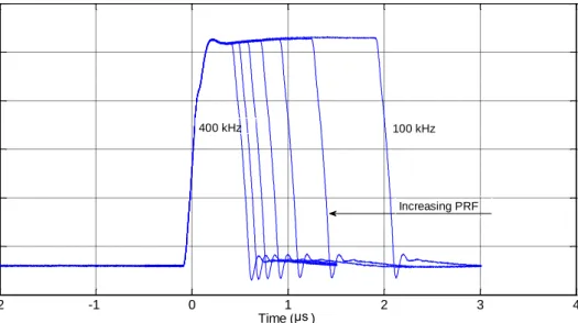
A comprehensive test plan (section 4.1) was devised which was aimed at evaluating the performance of the amplifiers when operated in pulsed mode. The test methodologies and setups utilised for such investigations are presented in chapter 4. The investigations focussed on determining achievable rise and fall times at pulse repetition frequencies (PRFs) of up to 450 kHz and on the detection of possible trapping effects which would affect pulse shape and power. A suitable gate-pulsing circuit was developed which could achieve rise and fall times characteristic of realistic radar systems (< 100ns). The principles of operation of the modulator are described in section 4.3 and its performance and improvements in section 5.2.
The amplifiers were subjected to a number of pulsed tests and examined both in the frequency and time domain. Fast sampling digital scopes (section 4.4.1) were utilised for time domain
9
characterisation of the amplifiers which is described in section 5.2. Frequency domain tests were carried out by means of Signal Analysers (section 4.4.2) and are illustrated in section 5.3.
New measures, such as Spectral Asymmetry and spectrum-derived Pulse Width Variation, are also introduced in section 5.3. Such measures may be useful performance indicators and avoid the need to resort to expensive instrumentation for high-frequency characterisation of pulsed amplifiers.
In addition device level tests (chapter 6) are also carried out on both Cree and Nitronex devices which investigate the presence of trapping effects through a bespoke pulsed I-V characterisation system designed to identify problems specific to GaN HEMTs technology. In Particular traps with release times of 100s of seconds and their effect on the operation of the devices when pulsed at typical radar PRFs are examined (section 6.5).
The author’s work investigated GaN devices both a transistor level and at amplifier level. The amplifier level work was carried out first, because of the limited device characterisation facilities available at Bristol University. Subsequently however the opportunity arose to carry out device level characterisation work with Sydney and Macquarie Universities, who had also been studying GaN devices but on a more fundamental level. This collaboration started when the author and Dr Rathmell of Sydney University met at EuMic 2009, where they presented papers in the same session. This collaborative work was seen by the author as the perfect opportunity to gain a deeper insight into GaN HEMTs operation and also to investigate how a customised pulsed I-V characterisation could aid the design of pulsed amplifiers and help understand amplifier performance shortcomings encountered during his tests at Bristol.
The work carried out by the author in Sydney allowed him to achieve a good understanding of transistor level issues which are often encountered with this technology. In addition this collaboration allowed him to conduct new experiments, bespoke to his pulsed applications, which highlighted new facts about the behaviour of GaN transistors when operated in pulsed mode, at typical Radar pulse repetition frequencies and duty cycles (section 6.5).
This work has raised considerable interest from the his sponsoring company MBDA Missile Systems and their partners, such as DMD5, who are eagerly awaiting the publication of the results and are considering setting up the appropriate facilities to carry out similar characterisation on their devices as a first step in the amplifier design process. To this end, Dr Rathmell and the author will present their work in December 2010 to DMD and MBDA.
5
10
1.5
Contributions Made
When the author first started researching wide bandgap semiconductor materials and GaN in particular, he found that relevant material on the physics of wide bandgap semiconductors was hard to come by. This made it difficult to understand the research papers on the topic, particularly considering that the work also appeared to be spread across a number of authors and research groups. The author’s first task was to compile a document which would give the GaN novice all the necessary material to get started and also provide a comprehensive review of GaN physics, technology, research status and commercial availability. This document, which is currently being considered by the IOP (Institute of Physics) for publication, provides information from the most relevant papers and books and a comprehensive list of references which will point the reader, who wishes to further investigate a specific topic, in the right direction. The document received very good reviews from Cree Inc, one of the leading manufacturers of GaN, who requested permission to use it within their organisation. The contents of this review document are summarised in chapters 2 and 3. The physical tests carried out confirmed the suitability of the GaN samples from Cree Inc to pulsed operation. The tests also highlighted important characterisation parameters which should be utilised in the design and performance enhancement of GaN amplifiers to be used in pulsed mode.
Through this work the author managed to:
- Design a modulator which could achieve high pulse repetition frequencies up to 450 kHz whilst maintaining rise and fall times below 100ns.
- Devise an unconventional modulating technique which greatly helps with the amplifier stability. This was achieved through pulsing the gate bias of the transistor instead of the drain bias which is what is normally done.
- Integrate data acquisition from instruments with signal processing through MatLab and its Instrument Control Toolbox. This allows for a cheaper implementation of the characterisation rig since most engineering companies already own MatLab licenses. It also makes the software and signal processing more easily modifiable since MatLab is now a universal tool which many engineers already use.
- Introduce zero-span measurements with Signal Analysers for pulse envelope recovery which allows for measurement to be made at carrier frequencies up to 26 GHz6.
- Introduce Spectral Imbalance and Pulse Width Deviation measurements which may help optimise the drive level and gate bias of the amplifier for maximum pulse fidelity and spectral symmetry.
6 Provided that the Signal Analyser has a resolution bandwidth which is wide enough to encompass most of
11
- Characterise achievable rise and fall times based on PRF and drive level.
- Prove that characteristic rise and fall times could be achieved with GaN amplifiers - Verify the absence of pulse envelope distortion due to current collapse and trapping
effects.
- Verify the existence of traps with release times of the order of 100s of seconds within the devices utilised but also the fact that such traps have no significant effects on the I-V characteristic of the devices at typical radar PRFs and duty cycles.
- Highlight the importance of using the appropriate I-V curve, based on the target operational PRF, when designing a pulsed amplifier with GaN HEMTs. The I-V curve was found to change significantly with the PRF.
The author’s research lead to following publications:
- Fornetti, F, Beach, MA & Morris, KA. 'Time and frequency domain analysis of commercial GaN HEMTs operated in pulsed mode', IEEE Asia Pacific Microwave Conference, 2009 (APMC 2009)
- Fornetti, F, Morris, KA & Beach, MA. 'Evaluation of commercial GaN HEMTS for pulsed power applications', IET European Pulsed Power Conference, 2009
- Fornetti, F, Morris, KA & Beach, MA. 'Pulsed operation and performance of commercial GaN HEMTs', 39th European Microwave Integrated Circuits Conference, 2009 (EuMIC 2009)
- Fornetti, F. ‘A review of high power solid state devices for microwave applications, materials, technology, research status and commercial availability’ (Awaiting Official Publication)
Forthcoming publications:
- A Review of High Power Solid State Devices for Microwave Applications: Materials, Technology, Research Status and Commercial Availability (Institute of Physics) - GaN Devices in Staggered-PRF Radar Systems (EuRad 2011)
The work carried out by the author has raised considerable interest from industry and it is now being implemented and improved for use in amplifier design and characterisation at MBDA, through a Knowledge Transfer Secondment.
12
2
Physics of Semiconductors and Heterojunctions
2.1
Introduction
Semiconductor devices have come a long way since they were first introduced as a replacement for vacuum tube devices. What was once a field dominated by Silicon and Germanium, has seen the introduction of several semiconductor alloys and in particular Gallium Arsenide (GaAs). This has enabled the fabrication of transistors with a frequency performance which would have been unachievable with other semiconductor materials. Despite the increase in the operating frequency however, the output power has remained limited and the generation of high RF power levels, of the order of 100’s to 1000’s of Watts is still difficult to achieve with solid state devices.
When it comes to power hungry systems such as radar, power-combining and/or phased array techniques need to be employed to achieve the required output levels with solid state devices, thus their application to such systems has so far been limited.
High power transmitters currently require the use of microwave vacuum tube devices. This is due to the fact that solid state devices are limited in the DC voltage that may be applied across their terminals when compared to vacuum devices. Such limitations are the direct consequence of the inherent critical field for breakdown that the semiconductor can sustain. A limited DC voltage means that high RF power operation can only be achieved with large DC and RF currents, which require large area devices. However large area devices have inherently high capacitance and low impedance, which limit the operating frequency. Series losses also become significant at the expense of efficiency [3].
Wide bandgap semiconductors such as SiC (Silicon Carbide), GaN (Gallium Nitride) and related heterostructures are characterised by a much higher breakdown voltage and therefore they may allow fabrication of devices with an order of magnitude improved RF output power compared to traditional solid state devices [4]. They have been the object of an extensive amount of research in the last decade and have now made their debut in the semiconductor devices market. GaN HEMTs (High electron Mobility Transistors) in particular are an increasingly popular choice when power, linearity and robustness are required.
Wide bandgap semiconductor devices however are currently limited in performance due to several physical effects associated with material-related and design-related issues. Nevertheless solutions to these problems are emerging, and these devices are now starting to find practical application [3]. In this chapter an overview of the properties of semiconductor materials is first presented. The physics of heterostructures and heterojunctions based on III-V semiconductor alloys is subsequently explored.
13
2.2
Semiconductor Materials and High Frequency Solid State Electronic
Devices
A major breakthrough in the development of semiconductor devices was the introduction of heterojunction growth technology which allows complex multiple layer device structures to be fabricated and optimized for maximized device performance. Technologies which permit the growth of epitaxial layers of precise thickness and impurity doping concentration (e.g. MBE7 and MOCVD8) have been developed and allow the fabrication of devices with layer thickness of only a few angstroms. This level of control permits devices with frequency performance well over 100–300 GHz to be fabricated [4].
The DC and RF performance capability of semiconductor devices is fundamentally dependent upon the electronic, thermal, and mechanical properties of the materials from which the devices are fabricated. In this section an overview of materials properties and their significance is presented along with the current technology status and a comparison of merits and demerits of various classes of devices.
Material Properties
Table 2.2-1 Main properties of semiconductor materials [4]
A summary of some of the semiconductor material properties most important to electronic device performance is listed in Table 2.2-1 for several semiconductors.
7 Molecular Beam Epitaxy
8
Metal-Organic Chemical Vapour Deposition
Material Eg (eV) εr Κ(W/°K-cm) Ec (V/m) Vacuum - 1 - - Si 1.12 11.9 1.5 3×10⁵ GaAs 1.43 12.5 0.54 4×10⁵ InP 1.34 12.4 0.67 4.5×10⁵ 3C-SiC 2.3 9.7 4 1.8×10⁶ 4H-SiC 3.2 10.0 4 3.5×10⁶ 6H-SiC 2.86 10.0 4 3.8×10⁶ GaN 3.4 9.5 1.3 2×10⁶ Diamond 5.6 5.5 20-30 5×10⁶
14
Desirable material properties include a large energy gap, Eg (eV), a low value of dielectric constant, εr, high thermal conductivity, κ (W/ºK-cm), and high critical electric field for breakdown Ec (V/cm).
Wide bandgap energy allows a material to withstand high internal electric fields before electronic breakdown occurs.
The dielectric constant gives an indication of the capacitive loading of a device and affects the terminal impedance. A low value for the semiconductor dielectric constant may reduce the capacitive loading and allows larger area devices to be fabricated for a specified impedance. Increased area permits larger RF currents and higher RF power to be generated [4].
The thermal conductance needs to be as high as possible in order to extract heat from the device efficiently. Diamond and SiC are excellent thermal conductors and have been used as substrates for GaN HEMTs [4].
Finally, the critical electric field for electronic breakdown should be high. This parameter is an indication of the strength of the electric fields that can be supported internally by the device before breakdown occurs. High electric fields permit large RF voltages to be supported, and hence high RF power to be generated. One of the attractive features of the wide bandgap materials is a high value for the critical field for breakdown, which is typically an order of magnitude greater than that of conventional semiconductors.
v-E Characteristics
A current is defined as the movement of charge and expressed as the product between the charge density and transport velocity. Therefore, the DC and RF currents that flow through a device are directly dependent upon the charge carrier velocity versus electric field transport characteristics of the semiconductor material. Generally, for high currents and high frequency, high charge carrier mobility and high saturation velocity are desirable. A comparison of the electron velocity-electric field v-E characteristics for several semiconductors is shown in Figure 2.2-1 [4].
The v-E characteristic is described in terms of charge carrier mobility μn (units of cm2/V·s), defined from the slope of the v-E characteristic at low electric field, and the saturated velocity vs (units of cm/sec), defined when the carrier velocity obtains a constant, field-independent magnitude, generally at high electric field. The high value for electron mobility of GaAs (typically, μn ~5000 cm2/V·s) is the main reason that FETs fabricated from this material have such excellent low noise and high-frequency performance [4].
15
Figure 2.2-1 Electron velocity vs. electric field characteristic for several semiconductors (Nd=1017cm-3)[4] In general, both high mobility and high saturation velocity are desirable for high RF current. Si and GaAs have electron saturation velocities that are limited to about vs = 1 х 107 cm/s, and this limits both the power that can be generated and the frequency response of the device. Wide bandgap semiconductors have electron saturation velocities that are a factor of two higher. The combination of high current and high voltage capability make wide bandgap semiconductors very attractive candidate materials for fabrication of high-power and high-performance electronic devices[4].
16
Technology StatusFigure 2.2-2 Average RF output power versus frequency for various electronic devices [4]
A large variety of semiconductor devices for high-frequency applications have been proposed, fabricated, demonstrated, and used in practical applications. A review of these devices has been presented in [5]. Figure 2.2-2 shows a comparison of state-of-the-art RF and microwave solid-state devices with microwave tubes. Solid-state devices produce RF power of about 100 W in S-band and 1W at 100 GHz. It is apparent that the output power and frequency range of solid-state devices is significantly lower than that obtainable from electronic vacuum tubes. The reduced RF power capability of solid-state devices is mainly due to:
1) Lower bias voltage that can be applied
2) Reduced electron velocity in the semiconductor which reduces the current and 3) The thermal limitation caused by the semiconductor thermal impedance
Solid-state RF output power can be increased by means of power combining techniques however the maximum power achievable is still limited to the 10’s to 100’s of kilowatt level in the microwave region. For megawatt systems it is difficult to efficiently combine the large number of devices necessary for practical systems.
17
The following list summarises the major merits (M) and drawbacks (D) of different microwave transistor types, together with some comments (C) [6]. The list has been restricted to devices that can or have the potential to work at high frequency.
GaAs MESFET
M Matured technology, simple device, low cost especially ion-implanted GaAs.
D Not well suited for operation above 20 GHz.
C Still important in both low-noise and power applications
GaAs HEMT
M Meanwhile matured technology. High operating frequency, low noise figure, reasonable output power
D Commonly a no ally-on device (needs a negative gate voltage to switch off), limited output power at high frequency.
C Most popular are the GaAs pHEMTs, conventional AlGaAs HEMTs are less important
GaAs HBT
M Relaxed requirements on lithography (no lateral submicron structures necessary) high linearity, high output power density
D Application in very low-power circuits problematic because of high emitter turn-on voltage
C Popular device for power amplification in cellular phones
InP HEMT
M Very high operating frequencies and frequency limits. Lowest noise figure of all microwave transistor types
D Expensive technology
C Application still limited to low-volume high-performance markets
InP HBT
M Highest operating frequencies and frequency limits of all bipolar transistors. Low emitter turn-on voltage (less than Si BJT, important for very-low-power applications)
18
C Application still limited to low-volume high-performance markets
Wide bandgap FETs (AlGaN/GaN HEMT, SiC MESFET)
M Highest output power density of all microwave FETs. High operating temperatures, high breakdown voltage
D Expensive and immature technology. Reliability still an open question
C SiC MESFETs commercially available but limited to X-band, AlGaN HEMTs commerciallyavailable at WiMax frequencies. Targeted application: power amplification at GHz frequencies.
19
2.4
Basic
Heterostructure
Physics
The development of heterostructures in the 1980s offered the opportunity of tremendous progress in the performance of microwave transistors. Such structures are now a key component in modern high-performance microwave devices such as HEMTs9 (High Electron Mobility Transistors) and HBTs (Heterostructure Bipolar transistors).
A heterostructure is a structure consisting of at least two layers of different semiconducting materials with distinct bandgaps. The interface between two of these layers is called a
heterojunction or heterointerface[6].
Figure 2.4-1 The Three Types of Heterostructure: (a) type I; (b) type II; (c) type III [6]
9
HEMTs are often called HFETs (Heterostructure Field Effect Transistors) in the literature
EC EV AlxGa1-xAs GaAs EC EV ∆EC ∆EV (a) EC EV Al0.48Ga0.52As InP EC EV ∆EC ∆EV (b) EC EV GaSb InAs EC EV ∆EC ∆EV (c) ∆EV
20
Consider two materials forming the heterostructure, materials 1 and 2, with energy gaps EG1 and EG2 respectively. Since the energy gaps are different, the conduction and valence bands of the two materials cannot be simultaneously continuous across the heterointerface. Generally, both the conduction band and valence band edges are discontinuous at a heterointerface. The energy differences between the conduction band and valence band edges at the interface are called the conduction and valence band offsets ∆EC and ∆EV.
Figure 2.4-1 shows the three different classes of heterostructures: type I, II, and III. The type I heterostructure (Figure 2.4-1.a) is the most common. An important example of a type I heterostructure is the GaAs-AlGaAs material system. Another important type I heterostructure, which is gaining increasing popularity in the semiconductor arena, is the GaN-AlGaN material system. In a type I heterostructure, the sum of the conduction band and valence band edge discontinuities is equal to the energy gap difference ∆EG
Eq. 2.4-1
The type II heterostructure (Figure 2.4-1.b) is arranged such that the discontinuities have different signs. The bandgap discontinuity in this case is given as the difference between the conduction band and valence band edge discontinuities. A typical type II heterostructure is formed by AlInAs and InP. In type III heterostructures (Figure 2.4-1.c), the band structure is such that the top of the valence band in one material lies above the conduction band minimum of the other material. An example of this type of heterostructure is that formed by GaSb and InAs (Figure 2.4-1.c ). As for the type II case, the bandgap discontinuity is equal to the difference between the conduction band and valence band edge discontinuities [7].
Figure 2.4-2 shows typical band diagrams and bandgap values for commonly used heterostructure systems. The bandgap difference and the band offsets are extremely important factors for the performance and operation of heterostructure devices such as HBTs and HEMTs [6].
Heterojunctions are subject to a further classification based on the atomic properties of their constituents namely, crystal type and lattice constants (see Appendix A, table A-1).
At the beginning of heterostructure research it was believed that only materials with nearly the same lattice constant could result in heterostructures useful for electron devices. However it was later realised that it is also possible to grow good quality heterostructures from materials with different lattice constants, provided the thickness of the grown layer does not exceed a certain critical value tc.
21
Figure 2.4-2 Band diagrams for different heterostructure pairs. (a)-(c) Type I, (d) Type II. The values of bandgaps and band offsets are in eV [7]
For layer thickness above the critical thickness, the lattice mismatch cannot be accommodated through strain, dislocations10
are produced and the strain relaxes as is seen in Figure 2.4-3b. If the grown layer is thinner than tc , its crystalline structure accommodates to that of the substrate material i.e. it adopts the lattice constant of the surrounding layers (Figure 2.4-3a). This causes a lattice deformation in the grown layer, and a pseudomorphic layer, frequently also called a strained layer, is created. This layer will be either compressed (compressive strain) or expanded (tensile strain) from its usual bulk crystal shape [6].
The amount of strain depends on the lattice mismatch between substrate and layer, and on the layer thickness. As an example, Figure 2.4-4 shows the schematic of a pseudomorphic AlGaAs/InGaAs/GaAs heterostructure in which the pseudomorphic InGaAs layer is under compressive strain [6].
Since GaAs and AlGaAs have a nearly identical lattice constant, it would appear counter intuitive to insert a mismatched layer between those two materials. This structure however can significantly improve electron mobility as explained in section 2.7.
10
Dislocations are crystal defects, or irregularities, within a crystal structure. They are linear defects around which some of the atoms of the crystal lattice are misaligned
1.80 Al0.48Ga0.52As GaAs 1.422 1.451 In0.52Al0.48As 0.737 In0.53Ga0.47As In0.53Ga0.47As 0.737 1.451 In0.52Al0.48As 1.353 InP 1.353 InP ∆EC = 0.219 ∆EV = 0.159 ∆EC = 0.271 ∆EV = 0.345 ∆EC = 0.52 ∆EV = 0.194 ∆EC = 0.253 ∆EV = 0.155 (a) (b) (c) (d)
22
(a) (b)
Heterointerface Epitaxial Layer
Figure 2.4-3 (a) Thin epitaxial layer strained to accommodate the various lattice constants of the underlying semiconductor layer and (b) a thicker epitaxial layer that has relaxed. In part (b) the epitaxial layer is thicker than the critical thickness and dislocations appear at the interface [6]
The third and newest kind of heterostructures currently used in microwave transistors is the so-called metamorphic type. The basic concept is to use a substrate material (e.g., GaAs) and to overgrow a graded buffer layer (e.g., InAlAs) with a thickness much greater than to tc. The buffer layer serves as a relaxed pseudo-substrate for the actual device layer. Because the buffer is extremely thick dislocations arising at the interface substrate/buffer barely influence the electrical properties of the device layer on top of the buffer. The main advantage of the metamorphic approach is that inexpensive GaAs substrates can be used to obtain high ∆EC values, and thus InP-HEMT-like performance can be attained with GaAs [6].
The use of heterostructures in high-speed devices resulted from the progress made in the epitaxial growth based on molecular beam epitaxy (MBE). Using MBE11
, it is possible to grow layers with a thickness of only a few nanometres and with sharp interfaces between the adjacent layers. Another epitaxial growth technique used to produce high-quality heterostructures for microwave transistors is metal organic chemical vapour deposition (MOCVD) [6].
11
23
Figure 2.4-4 Pseudomorphic heterostructure (on the right) consisting of the layer sequence AlGaAs-InGaAs-GaAs (on the left). The arrows indicate the compressive strain occurring in the pseudomorphic InGaAs layer[6]
24
2.5
Modulation Doping
Modulation doping offers an important advantage in device engineering since it provides a mechanism by which the free carrier concentration within a semiconductor layer can be increased significantly without the introduction of dopant impurities. Although conventional doping techniques can significantly increase the free carrier concentration and conductivity of a semiconductor, they come at the expense of increased ionized impurity scattering12
and a concomitant reduction in the carrier mobility and speed of the device.
Modulation doping on the other hand allows the free carrier concentration to be increased significantly without compromising the mobility. In a modulation-doped heterostructure, the free carriers are spatially separated from the dopants. The spatial separation of the dopants and free carriers reduces the deleterious action of ionized impurity scattering.
Modulation doping can be understood as follows. In its simplest implementation, one constructs a heterostructure formed by an n-type wide-bandgap semiconductor with an unintentionally doped, relatively narrow gap semiconductor, as shown in Figure 2.5-1(a).
The most commonly used materials systems for modulation doping are GaAs and AlGaAs. As shown in the diagram, the AlGaAs layer, which has the larger bandgap, is doped n-type, while the narrower gap GaAs layer is unintentionally doped13
.
In equilibrium the Fermi levels must align throughout the structure. When the two materials AlGaAs and GaAs are initially apart (Figure 2.5-1a), the Fermi level lies closer to the conduction band edge in the AlGaAs than in the GaAs since the AlGaAs is doped n-type. When the two materials are placed into contact, as shown in Figure 2.5-1(b), electrons must be transferred from the AlGaAs layer into the GaAs layer to align the Fermi level.
Another way to see this is that the conduction band on the AlGaAs side lies energetically higher than that on the GaAs side. Thus, the energy of the electrons in the conduction band of the AlGaAs layer is higher than that of the GaAs layer. Because electrons tend to occupy the lowest allowed energy state, they are encouraged to move from AlGaAs to GaAs. This results in a sizable increase in the electron concentration within the GaAs layer even without the introduction of ionized donor impurities.
12
Collisions and scattering by electrically charged impurities and crystal imperfections. The scattering probability decreases rapidly with increasing temperature because the faster-moving electron, on average, will spend less time near
the impurity. This reduces the scattering probability and increases the electron mobility. [8][8. Kwok, H.L., Electronic Materials. 1997: PWS.
13
25
Figure 2.5-1 (a) energy band diagrams of the AlGaAs and GaAs layers when apart and in equilibrium; (b) energy band diagram of the heterostructure. The two dashed horizontal lines at the heterointerface in the GaAs layer represent
energy subbands arising from spatial quantization effects [7]
The ionized donor atoms within the AlGaAs result in a net positive charge, which balances the net negative charge due to the electrons transferred in the GaAs layer. Although the ionized donor atoms in the AlGaAs obviously influence the electrons transferred in the GaAs, the spatial separation between the two charge species mitigates the Coulomb interaction between them. As a result, ionized impurity scattering of the transferred electrons is reduced, resulting in a higher electron mobility [7]. Ef AlGaAs GaAs Ef1 Ef2 (a) (b) Vacuum Level
26
2.6
Band Bending and Carrier Transport Parallel to Heterojunctions
Inspection of Figure 2.5-1(b) and Figure 2.6-1 shows that the conduction band edge in the GaAs layer is strongly bent near the heterointerface.
Figure 2.6-1 Expanded view of the conduction band edge discontinuity in the n-AlGaAs and i-GaAs heterojunction, showing two energy sub-bands. The energy sub-bands form due to spatial quantization effects in the heterostructure [7]
The band bending is a consequence of the electron transfer. The way in which the bands bend can be determined is as follows.
Consider AlGaAs, material 1 and GaAs material 2 respectively. If a Gaussian surface is drawn around the entire system, material 1 and 2, the net charge is zero. The system has to be space-charge neutral. Nevertheless, since there has been a net transfer of electrons from material 1 to 2, 2 has a net negative charge compared with 1. There is a positive charge in material 1 because of the ionized donors that precisely balance the negative charge due to the electron transfer. As an electron in material 1 approaches material 2, it sees a net negative charge that acts to raise its energy. Hence the bands bend upward from 1 to 2, as drawn in the diagram [9].
From the other side, as an electron is moved from 2 to 1, it sees a net positive charge due to the ionized donors present in material 1. Thus the closer the electron comes to material 1, the more net positive charge it sees, which reduces its energy. Hence the bands bend downward. The presence of the conduction-band-edge discontinuity forms a notch in the conduction band of the narrow-gap material, as shown in Figure 2.5-1b and Figure 2.6-1. Electrons within this region of the semiconductor are then confined by a triangular well-like potential [9].
27
Typically, the dimensions of this triangular well are very small, of the order of 10 nm or less, depending on the doping differential. Within this potential well spatial quantization effects occur [9]. Spatial quantization produces discrete energy bands, called sub-bands, in the potential well, as shown by the dashed lines in Figure 2.5-1b.
Figure 2.6-1 shows an expanded view of the conduction band edge formed at the interface of n-type AlGaAs and i-GaAs. The direction of quantization is perpendicular to the heterointerface (labelled as the z direction in Figure 2.6-1) and the energy along this direction is quantized. However, in the directions parallel to the interface (x and y), no spatial quantization effects occur since the motion of the electrons is not restricted by the band bending. Therefore, the electrons behave as free particles for motion along the x and y axes (those parallel to the interface) but are quantized in the direction perpendicular to the z direction. That is they can move only in a two-dimensional plane parallel to the heterointerface but not perpendicular to it because of the two potential barriers confining the potential well. Thus, these electrons constitute the so-called two-dimensional electron gas (2DEG)[7].
Figure 2.6-2 Band diagram of N+-AlGaAs/ p--GaAs heterojunction as used in AlGaAs/GaAs HEMTs under thermal equilibrium condition [6]
Now consider an N+-AlGaAs/ p--GaAs heterojunction. The + and - signs indicate that the AlGaAs and GaAs layers are heavily and lightly doped, respectively. This type of heterojunction is the heart of the conventionalAlGaAs/GaAsHEMT. The heavily doped layer with the higher conduction band is called the barrier layer, and the lightly doped layer with the lower conduction band is called the channel layer [6].
28
In this case holes also diffuse from the p-type channel layer to the barrier layer, although this effect is much less significant due to the presence of the valence band offset. Moreover a two-dimensional hole gas (2DHG) can be found at a p--GaAs/ N+-AlGaAs heterointerface. Because of their higher mobility, 2DEGs are far more popular and practical than 2DHGs in microwave transistors. Therefore, the following discussions are focused on 2DEGs[6].
Figure 2.6-2 also shows the space-charge region thickness dsc = dsc1 + dsc2. An electric field is present in the space-charge region which is mainly due to the uncompensated donor ions on the AlGaAs side and to the accumulated electrons on the GaAs side (which originally stem from the now uncompensated donor ions in the AlGaAs), and, to a much lesser extent, to the uncompensated acceptor ions on the GaAs side.
Frequently in HEMTs, a so-called spacer layer with a thickness dsp of a few nanometers is inserted between the heavily doped barrier layer and the lightly doped channel layer. The spacer consists of the same material as the barrier layer, i.e., AlGaAs in our example, and is undoped. It is used to further separate the 2DEG and ions in the AlGaAs layer, thereby enhancing the 2DEG mobility[6].
29
2.7
2DEG Mobility and Electron Sheet Density
The calculation of the electron density in a 2DEG differs from that in bulk material. To describe the electron density in a 2DEG, the 2DEG sheet density ns typically is used. Note that ns is in cm2, whereas the electron density n in bulk material is in cm3. The knowledge of the electron density in the 2DEG is essential for the description of the currents in a HEMT.
In structures consisting of doped AlGaAs and undoped GaAs layers, the electrons parallel to the heterointerfaces can have a much higher mobility compared to that in the doped bulk GaAs layers. Experimental results show that the 2DEG mobility is higher than the bulk mobility over a wide range of temperatures.
The increase in mobility compared to the bulk material is very significant at low temperatures (1 or more orders of magnitude) but much less pronounced at room temperature (a factor of two or less). The reason for the distinct mobility advantage of the AlGaAs/GaAs system at low temperatures is the fact that the 2DEG electrons located on the GaAs side are spatially isolated from the donor ions situated on the AlGaAs side of the heterojunction. Thus ionized impurity scattering (Coulomb scattering), which is the main limiting factor for mobility at low temperature, is reduced significantly in such a heterostructure. In a doped bulk GaAs, on the other hand, the ionized donors and the free electrons are not separated, and ionized impurity scattering is much more active.
The mobility however is influenced by several different scattering mechanisms (impurity, optical phonon, acoustic phonon, and surface roughness scattering) and at room temperature the main scattering mechanism limiting the mobility is not Coulomb scattering but optical phonon scattering. This mechanism is found in both the 2DEG and the bulk material. At room temperature the mobility is still higher in the 2DEG but just by a factor less than two [6].
When a spacer is introduced between the AlGaAs and GaAs layers, the separation between ionized donors and 2DEG electrons is increased, and the effect of Coulomb scattering can be further reduced. There is, however, a trade-off between spacer thickness and 2DEG sheet density. A thicker spacer layer leads to a higher mobility but a lower sheet density. It should be mentioned that microwave transistors are commonly operated at room temperature (or above when self heating is non negligible). Therefore the benefit of reduced Coulomb scattering in these devices is less than one would expect.
The mobility in III-V heterostructures can be increased considerably by replacing GaAs with InxGa1-xAs. Bulk lnxGa1-xAs possesses a higher electron mobility than bulk GaAs (i.e., zero In content), which translates into a higher 2DEG mobility [6].
30
Interestingly, the 2DEG mobilities in pseudomorphic GaAs HEMTs (the typical In content x is in the range of 0.15-0.25) are not necessarily higher than those in conventional AlGaAs HEMTs. This suggests that the strain in the InGaAs layer of these transistors has a detrimental effect on the mobility. However the choice of InGaAs instead of GaAs leads to a larger conduction band offset as well, and a larger ∆EC results in a higher sheet density [6].
A high mobility and a high 2DEG sheet density are design targets for HEMTs, which is why InGaAs layers with high In contents are widely used in high-performance HEMTs. It is desirable that these quantities be both large, thus giving a large product μ0 x ns. The incorporation of In, however, brings the drawback of a lower bandgap and thus a lower breakdown field in the lnGaAs layer [6].
31
3
GaN HEMTs: Physics, Limitations, Research Status and Commercial
availability
3.1
HEMTs: Structure and Characteristics
The main application of heterostructures is in High Electron Mobility Transistors (HEMTs). The high electron mobility and the low noise associated with the 2DEG are very useful for high-frequency and low-noise applications.
The 2DEG created at the AlGaAs-GaAs heterojunction makes the HEMT channel. As Figure 3.1-1 illustrates, contacts are fabricated at each end of the channel to create source and drain terminals. Also a gate in the form of a Schottky contact is created between the source and drain, to provide the means of controlling the device current [10].
Negative gate voltages reduce the electron concentration in the channel, and can completely repel the electrons, turning the device off. Therefore, the HEMT operates as a depletion-type FET. The transfer and output characteristics are analogous to those of the depletion-type MOSFET, JFET, and MESFET. Electrons pass through a couple of heterojunctions between the source terminal and the 2DEG, as well as between the 2DEG and the drain terminal. The energy-band diagrams shown in Figure 3.1-1 illustrate the barrier shapes associated with these heterojunctions at typical drain-to-source bias VDS [10].
It can be seen that electrons have to tunnel from the N+GaAs source into the N+AlGaAs layer, and tunnel again from the drain end of the 2DEG back into the N+AlGaAs layer. This introduces significant source and drain resistances, which adversely affect the high-speed and noise performance of the HEMT. Consequently, a number of modifications to source and drain contacts have been introduced to minimize the adverse effects of the source and drain resistances. The gate resistance is also very important, especially for noise performance. The gate is typically made in a mushroom shape (Figure 3.3-4) to decrease its resistance while not increasing the input capacitance, as well as improving the noise figure of the HEMT [10].
HEMTs have extremely high-frequency performance capability and very low noise performance, primarily due to the very high mobility characteristics of the 2DEG and RF operation up to 300 GHz has been demonstrated [4]. These devices are also used for microwave and mm-wave power applications and above X-band are superior to MESFETs.
The frequency response of a FET can be defined by the gain-bandwidth product and described by the device
f
T(GHz) as [10]L
v
C
g
f
s gs m T
2
2
Eq. 3.1-132
where vs (cm/s) is the saturation velocity of the electrons in the conducting channel, gm(mS) is the
device transconductance, Cgs(pF) is the gate-source capacitance, and
L
(μm) is the gate length.Figure 3.1-1 HEMT structure and energy bands at source and drain contacts [10]
High current gain and high-frequency response require short gate lengths and high electron saturation velocity. The former is controlled by the lithography and process technology employed to fabricate the gate and the latter is a function of the semiconductor (Figure 2.2-1). The highest frequency at which the transistor has positive gain is defined as the maximum frequency of oscillation fmaxand written in the form
g ds T
R
R
f
f
2
max
Eq. 3.1-2where Rdsis the drain/source resistance, and Rgis the gate resistance (Figure 3.11-1). A high fmax
requires a high
f
Tand a large ratioRds/Rg. Thef
T represents current gain and the ratio Rds/Rgrepresents voltage gain. Power gain can be obtained at frequencies above
f
T, but only byestablishing suitable voltage gain and this requires large output impedance to input impedance ratios. This is difficult to achieve at microwave frequencies and high performance mm-wave devices require high
f
T[4].![Figure 2.2-1 Electron velocity vs. electric field characteristic for several semiconductors (N d =10 17 cm -3 )[4]](https://thumb-us.123doks.com/thumbv2/123dok_us/680808.2582878/24.892.179.689.121.452/figure-electron-velocity-vs-electric-field-characteristic-semiconductors.webp)
![Figure 2.2-2 Average RF output power versus frequency for various electronic devices [4]](https://thumb-us.123doks.com/thumbv2/123dok_us/680808.2582878/25.892.143.718.164.526/figure-average-output-versus-frequency-various-electronic-devices.webp)
![Figure 3.3-3 Predicted RF performance for an AlGaN–GaN HEMT class amplifier at 100 GHz (V = 30 V, class A)[4]](https://thumb-us.123doks.com/thumbv2/123dok_us/680808.2582878/47.892.195.704.101.473/figure-predicted-performance-algan-hemt-class-amplifier-class.webp)
![Figure 3.7-2 Typical I–V characteristics showing load line drawn to maximize the area of the power triangle shown by the dotted lines [26]](https://thumb-us.123doks.com/thumbv2/123dok_us/680808.2582878/56.892.215.647.111.413/figure-typical-characteristics-showing-drawn-maximize-triangle-dotted.webp)
![Figure 3.10-2 AlGaN/GaN HEMT Structure and Sources of Operational Nonlinearities [3]](https://thumb-us.123doks.com/thumbv2/123dok_us/680808.2582878/63.892.180.720.306.619/figure-algan-gan-hemt-structure-sources-operational-nonlinearities.webp)
![Figure 3.10-3 HEMT Source Resistance Modulation Due to High Current Injection Conditions (V DS =8 v) [3]](https://thumb-us.123doks.com/thumbv2/123dok_us/680808.2582878/64.892.201.709.285.585/figure-hemt-source-resistance-modulation-current-injection-conditions.webp)
![Figure 3.11-1 AlGaN/GaN HEMT Equivalent Circuit with a Nonlinear Modulated Source Resistance Under High Current Injection Conditions [14]](https://thumb-us.123doks.com/thumbv2/123dok_us/680808.2582878/65.892.229.671.267.529/equivalent-circuit-nonlinear-modulated-resistance-current-injection-conditions.webp)
![Figure 3.11-2 Large-Signal Equivalent circuit Model Including Gate Tunnel Leakage Current Effect [14]](https://thumb-us.123doks.com/thumbv2/123dok_us/680808.2582878/66.892.174.710.145.503/figure-signal-equivalent-circuit-including-tunnel-leakage-current.webp)