DO NOT COPY
DO NOT COPY
DO NOT COPY
DO NOT COPY
DO NOT COPY
DO NOT COPY
DO NOT COPY
DO NOT COPY
DO NOT COPY
8.4 Counters
The name counter is generally used for any clocked sequential circuit whose state diagram contains a single cycle, as in Figure 8-26. The modulus of a counter is the number of states in the cycle. A counter with m states is called a
modulo-m counter or, sometimes, a divide-by-m counter. A counter with a
non-power-of-2 modulus has extra states that are not used in normal operation. HOW MUCH
DOES IT COST?
Once you understand the capabilities of different PLDs, you might ask, “Why not just always use the most capable PLD available?” For example, even if a circuit fits in a 20-pin 16V8, why not specify the slightly larger, 24-pin 20V8 so that spare inputs are available in case of trouble? And, once you’ve specified a 20V8, why not use the somewhat more capable 22V10 which comes in the same 24-pin package?
In the real world of product design and engineering, the constraint is cost. Otherwise, the argument of the previous paragraph could be extended ad nauseum, using CPLDs and FPGAs with even more capability (see \chapref{CPLDsFPGAs). Like automobiles and fine wines, digital devices such as PLDs, CPLDs, and FPGAs are not always priced proportionally to their capabilities and benefits. In particular, the closer a device’s capability is to the “bleeding edge,” the higher the premium you can expect to pay. Thus, when selecting a devices to realize a design, you must evaluate many trade-offs. For example, a high-density, high-cost CPLD or FPGA may allow a design to be realized in a single device whose internal functions are easily changed if need be. On the other hand, using two or more lower density PLDs, CPLDs, or FPGAs may save component cost but increase board area and power consumption, while making it harder to change the design later (since the device interconnections must be fixed when the board is fabricated).
What this goes to show is that overall cost must always be considered along with design elegance and convenience to create a successful (i.e., profitable) product. And minimizing the cost of a product usually involves a plethora of com-mon-sense economic and engineering considerations that are far removed from the turn-the-crank, algorithmic gate minimization methods of Chapter 4.
counter modulus S1 Sm S5 S4 S3 S2 Figure 8-26 General structure of a counter’s state diagram—a single cycle. modulo-m counter divide-by-m counter
DO NOT COPY
DO NOT COPY
DO NOT COPY
DO NOT COPY
DO NOT COPY
DO NOT COPY
DO NOT COPY
DO NOT COPY
DO NOT COPY
Probably the most commonly used counter type is an n-bit binary counter. Such a counter has n flip-flops and has 2n states, which are visited in the sequence 0, 1, 2, …, 2n−1, 0, 1, …. Each of these states is encoded as the corresponding n-bit binary integer.
8.4.1 Ripple Counters
An n-bit binary counter can be constructed with just n flip-flops and no other components, for any value of n. Figure 8-27 shows such a counter for n = 4. Recall that a T flip-flop changes state (toggles) on every rising edge of its clock input. Thus, each bit of the counter toggles if and only if the immediately preceding bit changes from 1 to 0. This corresponds to a normal binary counting sequence—when a particular bit changes from 1 to 0, it generates a carry to the next most significant bit. The counter is called a ripple counter because the carry information ripples from the less significant bits to the more significant bits, one bit at a time.
8.4.2 Synchronous Counters
Although a ripple counter requires fewer components than any other type of binary counter, it does so at a price—it is slower than any other type of binary counter. In the worst case, when the most significant bit must change, the output is not valid until time n ⋅ tpTQ after the rising edge of CLK, where tpTQ is the
propagation delay from input to output of a T flip-flop.
A synchronous counter connects all of its flip-flop clock inputs to the same common CLK signal, so that all of the flip-flop outputs change at the same time, after only tpTQ ns of delay. As shown in Figure 8-28, this requires the use of Tflip-flops with enable inputs; the output toggles on the rising edge of T if and only if EN is asserted. Combinational logic on the EN inputs determines which, if any, flip-flops toggle on each rising edge of T.
n-bit binary counter
Q Q T CLK T T T Q0 Q1 Q2 Q3 Q Q Q Q Q Q Figure 8-27 A 4-bit binary ripple counter. ripple counter synchronous counter
DO NOT COPY
DO NOT COPY
DO NOT COPY
DO NOT COPY
DO NOT COPY
DO NOT COPY
DO NOT COPY
DO NOT COPY
DO NOT COPY
As shown in Figure 8-28, it is also possible to provide a master count-enable signal CNTEN. Each T flip-flop toggles if and only if CNTEN is asserted and all of the lower-order counter bits are 1. Like the binary ripple counter, a synchronous n-bit binary counter can be built with a fixed amount of logic per bit—in this case, a T flip-flop with enable and a 2-input AND gate.
The counter structure in Figure 8-28 is sometimes called a synchronous
serial counter because the combinational enable signals propagate serially from
the least significant to the most significant bits. If the clock period is too short, there may not be enough time for a change in the counter’s LSB to propagate to the MSB. This problem is eliminated in Figure 8-29 by driving each EN input with a dedicated AND gate, just a single level of logic. Called a synchronous
parallel counter, this is the fastest binary counter structure.
Q T EN CLK CNTEN Q T Q T Q T Q0 Q1 Q2 Q3 EN EN EN Figure 8 -2 8 A synchronous 4-bit binary counter with serial enable logic.
synchronous serial counter Q T EN CLK CNTEN Q T Q T Q T Q0 Q1 Q2 Q3 EN EN EN Figure 8 -2 9 A synchronous 4-bit binary counter with parallel enable logic
synchronous parallel counter
DO NOT COPY
DO NOT COPY
DO NOT COPY
DO NOT COPY
DO NOT COPY
DO NOT COPY
DO NOT COPY
DO NOT COPY
DO NOT COPY
8.4.3 MSI Counters and Applications
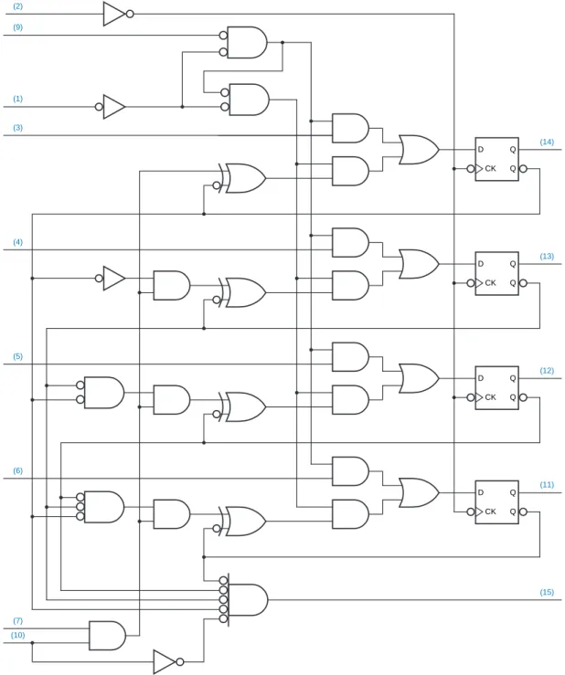
The most popular MSI counter is the 74x163, a synchronous 4-bit binary counter with active-low load and clear inputs, with the traditional logic symbol shown in Figure 8-30. Its function is summarized by the state table in Table 8-11, and its internal logic diagram is shown in Figure 8-31.
The ’163 uses D flip-flops rather than T flip-flops internally to facilitate the load and clear functions. Each D input is driven by a 2-input multiplexer consist-ing of an OR gate and two AND gates. The multiplexer output is 0 if the CLR_L input is asserted. Otherwise, the top AND gate passes the data input (A, B, C, orD) to the output if LD_L is asserted. If neither CLR_L nor LD_L is asserted, the bottom AND gate passes the output of an XNOR gate to the multiplexer output.
Ta b l e 8 - 1 1 State table for a 74x163 4-bit binary counter.
Inputs Current State Next State
CLR_L LD_L ENT ENP QD QC QB QA QD∗ QC∗ QB∗ QA∗ 0 x x x x x x x 0 0 0 0 1 0 x x x x x x D C B A 1 1 0 x x x x x QD QC QB QA 1 1 x 0 x x x x QD QC QB QA 1 1 1 1 0 0 0 0 0 0 0 1 1 1 1 1 0 0 0 1 0 0 1 0 1 1 1 1 0 0 1 0 0 0 1 1 1 1 1 1 0 0 1 1 0 1 0 0 1 1 1 1 0 1 0 0 0 1 0 1 1 1 1 1 0 1 0 1 0 1 1 0 1 1 1 1 0 1 1 0 0 1 1 1 1 1 1 1 0 1 1 1 1 0 0 0 1 1 1 1 1 0 0 0 1 0 0 1 1 1 1 1 1 0 0 1 1 0 1 0 1 1 1 1 1 0 1 0 1 0 1 1 1 1 1 1 1 0 1 1 1 1 0 0 1 1 1 1 1 1 0 0 1 1 0 1 1 1 1 1 1 1 0 1 1 1 1 0 1 1 1 1 1 1 1 0 1 1 1 1 1 1 1 1 1 1 1 1 0 0 0 0 74x163 74x163 CLR CLK LD QA QB 2 14 11 1 9 ENP ENT 7 10 A B 3 4 C D 5 6 QC QD 15 RCO 13 12 Figure 8-30 Traditional logic symbol for the 74x163.
DO NOT COPY
DO NOT COPY
DO NOT COPY
DO NOT COPY
DO NOT COPY
DO NOT COPY
DO NOT COPY
DO NOT COPY
DO NOT COPY
Q Q CLK CK D (14) QA Q Q CK D (13) QB Q Q CK D (12) QC Q Q CK D (11) QD RCO (15) (6) D (7) ENP (10) ENT (5) C (4) B (3) A (1) CLR_L (9) (2) LD_LFigure 8-31 Logic diagram for the 74x163 synchronous 4-bit binary counter, including pin numbers for a standard 16-pin dual in-line package.
DO NOT COPY
DO NOT COPY
DO NOT COPY
DO NOT COPY
DO NOT COPY
DO NOT COPY
DO NOT COPY
DO NOT COPY
DO NOT COPY
The XNOR gates perform the counting function in the ’163. One input of each XNOR is the corresponding count bit (QA, QB, QC, or QD); the other input is 1, which complements the count bit, if and only if both enables ENP and ENT are asserted and all of the lower-order count bits are 1. The RCO (“ripple carry out”) signal indicates a carry from the most significant bit position, and is 1 when all of the count bits are 1 and ENT is asserted.
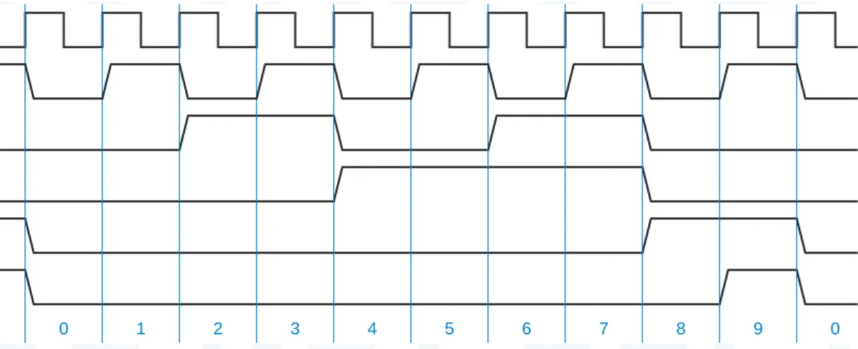
Even though most MSI counters have enable inputs, they are often used in a free-running mode in which they are enabled continuously. Figure 8-32 shows the connections to make a ’163 operate in this way, and Figure 8-33 shows the resulting output waveforms. Notice that starting with QA, each signal has half the frequency of the preceding one. Thus, a free-running ’163 can be used as a divide-by-2, -4, -8, or -16 counter, by ignoring any unnecessary high-order output bits.
Note that the ’163 is fully synchronous; that is, its outputs change only on the rising edge of CLK. Some applications need an asynchronous clear function, free-running counter 74x163 CLR CLK LD QA QB 2 14 11 1 9 ENP ENT 7 10 A QA QB QC QD RCO B 3 4 C D 5 6 QC QD 15 RCO U1 13 12 CLOCK RPU +5 V R Figure 8-32 Connections for the 74x163 to operate in a free-running mode. CLK QA QB QC QD COUNT 0 1 2 3 4 5 6 7 8 9 10 11 12 13 14 15 0 RCO
DO NOT COPY
DO NOT COPY
DO NOT COPY
DO NOT COPY
DO NOT COPY
DO NOT COPY
DO NOT COPY
DO NOT COPY
DO NOT COPY
as provided by the 74x161. The ’161 has the same pinout as the ’163, but itsCLR_L input is connected to the asynchronous clear inputs of its flip-flops. The 74x160 and 74x162 are more variations with the same pinouts and general functions as the ’161 and ’163, except that the counting sequence is modified to go to state 0 after state 9. In other words, these are modulo-10 counters, sometimes called decade counters. Figure 8-34 shows the output waveforms for a free-running ’160 or ’162. Notice that although the QD and QC outputs have one-tenth of the CLK frequency, they do not have a 50% duty cycle, and the QC output, with one-fifth of the input frequency, does not have a constant duty cycle. We’ll show the design of a divide-by-10 counter with a 50% duty-cycle output later in this subsection.
Although the ’163 is a modulo-16 counter, it can be made to count in a modulus less than 16 by using the CLR_L or LD_L input to shorten the normal counting sequence. For example, Figure 8-35 shows one way of using the ’163 as a modulo-11 counter. The RCO output, which detects state 15, is used to force
74x161 74x160 74x162 decade counter CLOCK QA QB QC QD COUNT 0 1 2 3 4 5 6 7 8 9 0 RCO
Figure 8-34 Clock and output waveforms for a free-running divide-by-10 counter.
74x163 74x04 CLR CLK LD QA QB 2 14 11 1 1 9 ENP ENT 7 10 A Q0 Q1 Q2 Q3 B 3 4 C D 5 6 QC QD 15 2 RCO 13 12 CNT15 CNT15_L U1 U2 CLOCK RPU +5 V R Figure 8-35 Using the 74x163 as a modulo-11 counter with the counting sequence 5, 6, …, 15, 5, 6, ….
DO NOT COPY
DO NOT COPY
DO NOT COPY
DO NOT COPY
DO NOT COPY
DO NOT COPY
DO NOT COPY
DO NOT COPY
DO NOT COPY
the next state to 5, so that the circuit will count from 5 to 15 and then start at 5 again, for a total of 11 states per counting cycle.
A different approach for modulo-11 counting with the ’163 is shown in Figure 8-36. This circuit uses a NAND gate to detect state 10 and force the next state to 0. Notice that only a 2-input gate is used to detect state 10 (binary 1010). Although a 4-input gate would normally be used to detect the condition CNT10
=Q3 ⋅ Q2′⋅ Q1 ⋅ Q0′, the 2-input gate takes advantage of the fact that no other state in the normal counting sequence of 0–10 has Q3 = 1 and Q1 = 1. In general, to detect state N in a binary counter that counts from 0 to N, we need to AND only the state bits that are 1 in the binary encoding of N.
There are many other ways to make a modulo-11 counter using a ’163. The choice of approach—one of the preceding or a combination of them (as in Exercise 8.25)—depends on the application. As another example, in Section 2.10 we promised to show you how to build a circuit that counts in the
74x163 74x00 CLR CLK LD QA QB 2 14 11 1 1 2 9 ENP ENT 7 10 A Q0 Q1 Q2 Q3 B 3 4 C D 5 6 QC QD 15 3 RCO 13 12 CNT10_L U1 U2 CLOCK RPU +5 V R Figure 8-36 Using the 74x163 as a modulo-11 counter with the counting sequence 0, 1, 2, …, 10, 0, 1, …. 74x163 74x00 CLR CLK LD QA QB 2 14 11 1 1 2 9 ENP ENT 7 10 A Q0 Q1 Q2 Q3 B C D QC QD 15 3 RCO 13 12 S11XX_L U1 U2 +5 V CLOCK RPU R 3 4 5 6 Figure 8-37 A 74x163 used as an excess-3 decimal counter.
DO NOT COPY
DO NOT COPY
DO NOT COPY
DO NOT COPY
DO NOT COPY
DO NOT COPY
DO NOT COPY
DO NOT COPY
DO NOT COPY
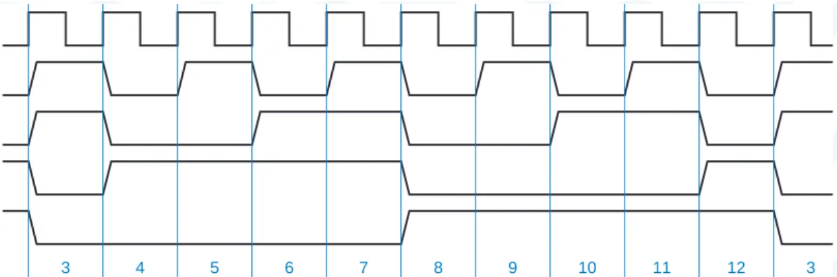
excess-3 decimal code, shown in Table 2-9 on page 45. Figure 8-37 shows theconnections for a ’163 to count in the excess-3 sequence. A NAND gate detects state 1100 and forces 0011 to be loaded as the next state. Figure 8-38 shows the resulting timing waveforms. Notice that the Q3 output has a 50% duty cycle, which may be desirable for some applications.
A binary counter with a modulus greater than 16 can be built by cascading 74x163s. Figure 8-39 shows the general connections for such a counter. The CLK, CLR_L, and LD_L inputs of all the ’163s are connected in parallel, so that all of them count or are cleared or loaded at the same time. A master count-enable (CNTEN) signal is connected to the low-order ’163. The RCO4 output is asserted if and only if the low-order ’163 is in state 15 and CNTEN is asserted; RCO4 is connected to the enable inputs of the high-order ’163. Thus, both the carry information and the master count-enable ripple from the output of one
CLOCK Q0 Q1 Q2 Q3 COUNT 3 4 5 6 7 8 9 10 11 12 3
Figure 8-38 Timing waveforms for the ’163 used as an excess-3 decimal counter.
74x163 CLR CLK LD QA QB 2 14 11 1 9 ENP ENT 7 10 A Q0 Q1 Q2 Q3 B 3 4 C D 5 6 Q4 Q5 Q6 Q7 RCO8 QC QD 15 RCO 13 12 U1 74x163 CLR CLK LD QA QB 2 1 9 14 11 ENP ENT 7 10 A B 3 4 C D 5 6 QC QD 15 RCO 13 12 U2 CLOCK RESET_L D0 D1 D2 D3 D4 D5 D6 D7 LOAD_L CNTEN RCO4
DO NOT COPY
DO NOT COPY
DO NOT COPY
DO NOT COPY
DO NOT COPY
DO NOT COPY
DO NOT COPY
DO NOT COPY
DO NOT COPY
4-bit counter stage to the next. Like the synchronous serial counter of Figure 8-28, this scheme can be extended to build a counter with any desired number of bits; the maximum counting speed is limited by the propagation delay of the ripple carry signal through all of the stages (but see Exercise 8.27).
Even experienced digital designers are sometimes confused about the difference between the ENP and ENT enable inputs of the ’163 and similar counters, since both must be asserted for the counter to count. However, a glance at the 163’s internal logic diagram, Figure 8-31 on page 597, shows the difference quite clearly—ENT goes to the ripple carry output as well. In many applications, this distinction is important.
For example, Figure 8-40 shows an application that uses two ’163s as a modulo-193 counter that counts from 63 to 255. The MAXCNT output detects state 255 and stops the counter until GO_L is asserted. When GO_L is asserted, the counter is reloaded with 63 and counts up to 255 again. (Note that the value of GO_L is relevant only when the counter is in state 255.) To keep the counter
74x163 CLR CLK LD QA QB 2 14 11 1 9 1 9 ENP ENT 7 10 A Q0 Q1 Q2 Q3 B 3 4 6 C D 5 4 5 3 1 2 6 Q4 Q5 Q6 Q7 MAXCNT QC QD 15 RCO 13 12 U2 U1 U1 74x163 CLR CLK LD QA QB 2 14 11 ENP ENT 7 10 A B 3 4 C D 5 6 QC QD 15 RCO 13 12 U3 CLOCK RESET_L GO_L RELOAD_L CNTEN RPU 74x00 74x00 +5 V R RCO4 Figure 8-40 Using 74x163s as a modulo-193 counter with the counting sequence 63, 64, …, 255, 63, 64, ….
DO NOT COPY
DO NOT COPY
DO NOT COPY
DO NOT COPY
DO NOT COPY
DO NOT COPY
DO NOT COPY
DO NOT COPY
DO NOT COPY
stopped, MAXCNT must be asserted in state 255 even while the counter isstopped. Therefore, the low-order counter’s ENT input is always asserted, its RCO output is connected to the high-order ENT input, and MAXCNT detects state 255 even if CNTEN is not asserted (compare with the behavior of RCO8 in Figure 8-39). To enable counting, CNTEN is connected to the ENP inputs in parallel. A NAND gate asserts RELOAD_L to go back to state 63 only if GO_L is asserted and the counter is in state 255.
Another counter with functions similar to 74x163’s is the 74x169, whose logic symbol is shown in Figure 8-41. One difference in the ’169 is that its carry output and enable inputs are active low. More importantly, the ’169 is an up/
down counter; it counts in ascending or descending binary order depending on
the value of an input signal, UP/DN. The ’169 counts up when UP/DN is 1 and down when UP/DN is 0.
8.4.4 Decoding Binary-Counter States
A binary counter may be combined with a decoder to obtain a set of 1-out-of-m-coded signals, where one signal is asserted in each counter state. This is useful when counters are used to control a set of devices where a different device is enabled in each counter state. In this approach, each output of the decoder enables a different device.
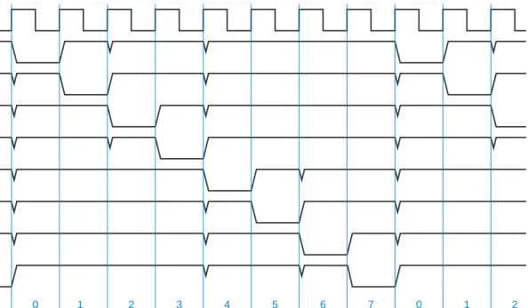
Figure 8-42 shows how a 74x163 wired as a modulo-8 counter can be com-bined with a 74x138 3-to-8 decoder to provide eight signals, each one representing a counter state. Figure 8-43 shows typical timing for this circuit. Each decoder output is asserted during a corresponding clock period.
Notice that the decoder outputs may contain “glitches” on state transitions where two or more counter bits change, even though the ’163 outputs are glitch free and the ’138 does not have any static hazards. In a synchronous counter like the ’163, the outputs don’t change at exactly the same time. More important,
74x169 74x169 UP/DN CLK LD QA QB 2 14 11 1 9 ENP ENT 7 10 A B 3 4 C D 5 6 QC QD 15 RCO 13 12 Fi gure 8-41 Logic symbol for the 74x169 up/down counter. up/down counter 74x163 CLR CLK LD QA QB 2 14 11 1 9 ENP ENT 7 10 A Q1 Q2 Q3 B 3 4 C D 5 6 QC QD 15 RCO U1 13 12 CLOCK RPU +5 V R S0_L S1_L S2_L S3_L S4_L S5_L S6_L S7_L 74x138 G2A G1 G2B Y0 Y1 Y2 Y3 6 15 14 13 7 4 5 B A C Y4 Y5 Y6 Y7 1 12 11 10 9 2 3 U2 Figure 8-42 A modulo-8 binary counter and decoder. decoding glitches
DO NOT COPY
DO NOT COPY
DO NOT COPY
DO NOT COPY
DO NOT COPY
DO NOT COPY
DO NOT COPY
DO NOT COPY
DO NOT COPY
multiple signal paths in a decoder like the ’138 have different delays; for exam-ple, the path from B to Y1_L is faster than the path from A to Y1_L. Thus, even if the input changes simultaneously from 011 to 100, the decoder may behave as if the input were temporarily 001, and the Y1_L output may have a glitch. In the present example, it can be shown that the glitches can occur in any realization of the binary decoder function; this problem is called a function hazard.
In most applications, the decoder output signals portrayed in Figure 8-43 would be used as control inputs to registers, counters, and other edge-triggered devices (e.g., EN_L in a 74x377, LD_L in a 74x163, or ENP_L in a 74x169). In such a case, the decoding glitches in the figure are not a problem, since they occur after the clock tick. They are long gone before the next tick comes along, when the decoder outputs are sampled by other edge-triggered devices. However, the glitches would be a problem if they were applied to something like the S_L or R_L inputs of an S-R latch. Likewise, using such potentially glitchy signals as clocks for edge-triggered devices is a definite no-no.
If necessary, one way to “clean up” the glitches in Figure 8-43 is to connect the ’138 outputs to another register that samples the stable decoded outputs on the next clock tick, as shown in Figure 8-44. Notice that the decoded outputs have been renamed to account for the 1-tick delay through the register. However, once you decide to pay for an 8-bit register, a less costly solution is to use an 8-bit “ring counter,” which provides glitch-free decoded outputs directly, as we’ll show in Section 8.5.6.
CLOCK_L S0_L S1_L S2_L S3_L S4_L S5_L S6_L S7_L COUNT 0 1 2 3 4 5 6 7 0 1 2
Figure 8-43 Timing diagram for a modulo-8 binary counter and decoder, showing decoding glitches.
DO NOT COPY
DO NOT COPY
DO NOT COPY
DO NOT COPY
DO NOT COPY
DO NOT COPY
DO NOT COPY
DO NOT COPY
DO NOT COPY
8.4.5 Counters in ABEL and PLDsBinary counters are good candidates for ABEL- and PLD-based design, for several reasons:
• A large state machine can often be decomposed into two or more smaller state machines where one of the smaller machines is a binary counter that keeps track of how long the other machine should stay in a particular state. This may simplify both the conceptual design and the circuit design of the machine.
• Many applications require almost-binary-modulus counters with special requirements for initialization, state detection, or state skipping. For exam-ple, a counter in an elevator controller may skip state 13. Instead of using an off-the-shelf binary counter and extra logic for the special requirements, a designer can specify exactly the required functions in an ABEL program. • Most standard MSI counters have only 4 bits, while a single 24-pin PLD
can be used to create a binary counter with up to 10 bits.
The most popular MSI counter is the 74x163 4-bit binary counter, shown in Figure 8-31 on page 597. A glance at this figure shows that the excitation logic for this counter isn’t exactly simple, especially considering its use of XNOR gates. Nevertheless, ABEL provides a very simple way of defining counter behavior, which we describe next.
Recall that ABEL uses the “+” symbol to specify integer addition. When two sets are “added” with this operator, each is interpreted as a binary number; the rightmost set element corresponds to the least significant bit of the number. Thus, the function of a 74x163 can be specified by the ABEL program in Table 8-12. When the counter is enabled, 1 is added to the current state.
74x163 CLR CLK LD QA QB 2 14 11 1 9 ENP ENT 7 10 A Q1 Q2 Q3 B 3 4 C D 5 6 QC QD 15 RCO U1 13 12 CLOCK RPU +5 V R S0_L S1_L S2_L S3_L S4_L S5_L S6_L S7_L RS0_L RS1_L RS2_L RS3_L RS4_L RS5_L RS6_L RS7_L 74x138 G2A G1 G2B Y0 Y1 Y2 Y3 6 15 14 13 7 4 5 B A C Y4 Y5 Y6 Y7 1 12 11 10 9 2 3 U2 U3 74x374 OE CLK 1D 1Q 11 1 2 2Q 5 3 2D 4 3D 7 4D 8 5D 13 6D 14 3Q 6 9 5Q 12 15 4Q 6Q 7D 17 16 7Q 8D 18 19 8Q
DO NOT COPY
DO NOT COPY
DO NOT COPY
DO NOT COPY
DO NOT COPY
DO NOT COPY
DO NOT COPY
DO NOT COPY
DO NOT COPY
T a b l e 8 - 1 2 ABEL program for a 74x163-like 4-bit binary counter.
module Z74X163
title '4-bit Binary Counter' " Input pins
CLK, !LD, !CLR, ENP, ENT pin; A, B, C, D pin; " Output pins
QA, QB, QC, QD pin istype 'reg'; RCO pin istype 'com'; " Set definitions
INPUT = [D, C, B, A]; COUNT = [QD, QC, QB, QA]; equations
COUNT.CLK = CLK;
COUNT := !CLR & ( LD & INPUT
# !LD & (ENT & ENP) & (COUNT + 1) # !LD & !(ENT & ENP) & COUNT); RCO = (COUNT == [1,1,1,1]) & ENT;
end Z74X163
T a b l e 8 - 1 3 MInimized equations for the 4-bit binary counter in page 606.
QA := (CLR & LD & ENT & ENP & !QA # CLR & LD & !ENP & QA # CLR & LD & !ENT & QA # CLR & !LD & A);
QB := (CLR & LD & ENT & ENP & !QB & QA # CLR & LD & QB & !QA
# CLR & LD & !ENP & QB # CLR & LD & !ENT & QB # CLR & !LD & B);
QC := (CLR & LD & ENT & ENP & !QC & QB & QA # CLR & LD & QC & !QA
# CLR & LD & QC & !QB # CLR & LD & !ENP & QC # CLR & LD & !ENT & QC # CLR & !LD & C);
QD := (CLR & LD & ENT & ENP & !QD & QC & QB & QA # CLR & !LD & D
# CLR & LD & QD & !QB # CLR & LD & QD & !QC # CLR & LD & !ENP & QD # CLR & LD & !ENT & QD # CLR & LD & QD & !QA); RCO = (ENT & QD & QC & QB & QA);
DO NOT COPY
DO NOT COPY
DO NOT COPY
DO NOT COPY
DO NOT COPY
DO NOT COPY
DO NOT COPY
DO NOT COPY
DO NOT COPY
Table 8-13 shows the minimized logic equations that ABEL generates for the 4-bit counter. Notice that each more significant output bit requires one more product term. As a result, the size of counters that can be realized in a 16V8 or even a 20V8 is generally limited to five or six bits. Other devices, including the X-series PLDs and some CPLDs, contain an XOR structure that can realize larger counters without increasing product-term requirements.
Designing a specialized counting sequence in ABEL is much simpler than adapting a standard binary counter. For example, the ABEL program in Table 8-12 can be adapted to count in excess-3 sequence (Figure 8-38 on page 601) by changing the equations as follows:
COUNT := !CLR & ( LD & INPUT # !LD & (ENT & ENP) &
((COUNT==12) & 3) # ((COUNT!=12) & (COUNT + 1)) # !LD & !(ENT & ENP) & COUNT);
RCO = (COUNT == 12) & ENT;
PLDs can be cascaded to obtain wider counters, by providing each counter stage with a carry output that indicates when it is about to roll over. There are two basic approaches to generating the carry output:
• Combinational. The carry equation indicates that the counter is enabled
and is currently in its last state before rollover. For a 5-bit binary up counter, we have
COUT = CNTEN & Q4 & Q3 & Q2 & Q1 & Q0;
Since CNTEN is included, this approach allows carries to be rippled through cascaded counters by connecting each COUT to the next CNTEN.
• Registered. The carry equation indicates that the counter is about to enter
its last state before rollover. Thus, at the next clock tick, the counter enters this last state and the carry output is asserted. For a 5-bit binary up counter with load and clear inputs, we have
COUT := !CLR & !LD & CNTEN
& Q4 & Q3 & Q2 & Q1 & !Q0 # !CLR * !LD * !CNTEN
& Q4 & Q3 & Q2 & Q1 & Q0 # !CLR & LD
& D4 & D3 & D2 & D1 & D0;
The second approach has the advantage of producing COUT with less delay than the combinational approach. However, external gates are now required between stages, since the CNTEN signal for each stage should be the logical AND of the master count-enable signal and the COUT outputs of all lower-order counters. These external gates can be avoided if the higher-order counters have multiple enable inputs.
combinational carry output
DO NOT COPY
DO NOT COPY
DO NOT COPY
DO NOT COPY
DO NOT COPY
DO NOT COPY
DO NOT COPY
DO NOT COPY
DO NOT COPY
8.4.6 Counters in VHDLLike ABEL, VHDL allows counters to be specified fairly easily. The biggest challenge in VHDL, with its strong type checking, is to get all of the signal types defined correctly and consistently.
Table 8-14 is a VHDL program for a 74x163-like binary counter. Notice that the program uses the IEEE.std_logic_arith.all library, which includes the UNSIGNED type, as we described in Section 5.9.6 on page 389. This library includes definitions of “+” and “-” operators that perform unsigned addition and subtraction on UNSIGNED operands. The counter program declares the counter input and output as UNSIGNED vactors and uses “+” to increment the counter value as required.
In the program, we defined an internal signal IQ to hold the counter value. We could have used Q directly, but then we’d have to declare its port type as buffer rather than out. Also, we could have defined the type of ports D and Q to be STD_LOGIC_VECTOR, but then we would have to perform type conversions inside the body of the process (see Exercise 8.33).
T a b l e 8 - 1 4 VHDL program for a 74x163-like 4-bit binary counter.
library IEEE;
use IEEE.std_logic_1164.all; use IEEE.std_logic_arith.all; entity V74x163 is
port ( CLK, CLR_L, LD_L, ENP, ENT: in STD_LOGIC; D: in UNSIGNED (3 downto 0);
Q: out UNSIGNED (3 downto 0); RCO: out STD_LOGIC );
end V74x163;
architecture V74x163_arch of V74x163 is signal IQ: UNSIGNED (3 downto 0); begin
process (CLK, ENT, IQ) begin
if (CLK'event and CLK='1') then
if CLR_L='0' then IQ <= (others => '0'); elsif LD_L='0' then IQ <= D;
elsif (ENT and ENP)='1' then IQ <= IQ + 1; end if;
end if;
if (IQ=15) and (ENT='1') then RCO <= '1'; else RCO <= '0';
end if; Q <= IQ; end process; end V74x163_arch;
DO NOT COPY
DO NOT COPY
DO NOT COPY
DO NOT COPY
DO NOT COPY
DO NOT COPY
DO NOT COPY
DO NOT COPY
DO NOT COPY
As in ABEL, specialized counting sequences can be specified very easily using behavioral VHDL code. For example, Table 8-15 modifies the 74x163-like counter to count in excess-3 sequence (3, … , 12, 3, … ).
Unfortunately, some VHDL synthesis engines do not synthesize counters particularly well. In particular, they tend to synthesize the counting step using a binary adder with the counter value and a constant 1 as operands. This approach requires much more combinational logic than what we’ve shown for discrete counters, and is particularly wasteful in CPLDs and FPGAs containing T flip-flops, XOR gates, or other structures optimized for counters. In this case, a useful alternative is to write structural VHDL that is targeted to the cells available in a particular CPLD, FPGA, or ASIC technology.
For example, we can construct one bit-cell for a 74x163-like counter using the circuit in Figure 8-45. This circuit is designed to use serial propagation for the carry bits, so the same circuit can be used at any stage of an arbitrarily large counter, subject to fanout constraints on the common signals that drive all of the stages. The signals in the bit-cell have the following definitions:
CLK (common) The clock input for all stages.
LDNOCLR (common) Asserted if the counter’s LD input is asserted and CLR is negated.
NOCLRORLD (common) Asserted if the counter’s CLR and LD inputs are both negated.
CNTENP (common) Asserted if the counter’s ENP input is asserted. Di (per cell) Load data input for cell i.
T a b l e 8 - 1 5 VHDL architecture for counting in excess-3 order.
architecture V74xs3_arch of V74x163 is signal IQ: UNSIGNED (3 downto 0); begin
process (CLK, ENT, IQ) begin
if CLK'event and CLK='1' then
if CLR_L='0' then IQ <= (others => '0'); elsif LD_L='0' then IQ <= D;
elsif (ENT and ENP)='1' and (IQ=12) then IQ <= ('0','0','1','1'); elsif (ENT and ENP)='1' then IQ <= IQ + 1;
end if; end if;
if (IQ=12) and (ENT='1') then RCO <= '1'; else RCO <= '0';
end if; Q <= IQ; end process; end V74xs3_arch;
DO NOT COPY
DO NOT COPY
DO NOT COPY
DO NOT COPY
DO NOT COPY
DO NOT COPY
DO NOT COPY
DO NOT COPY
DO NOT COPY
CNTENi (per cell) Serial count enable input for cell i. CNTENi+1 (per cell) Serial count enable output for cell i.
Qi (per cell) Counter output for cell i.
Table 8-16 is a VHDL program corresponding to the bit-cell in the figure. In the program, the D flip-flop component Vdffqqn is assumed to be already defined; it is similar to the D flip-flop in Table 8-6 with the addition of a QN (complemented) output. In an FPGA or ASIC design, a flip-flop component type would be chosen from the manufacturer’s standard cell library.
T a b l e 8 - 1 6 VHDL program for counter cell of Figure 8-45.
library IEEE;
use IEEE.std_logic_1164.all; entity syncsercell is
port( CLK, LDNOCLR, NOCLRORLD, CNTENP, D, CNTEN: in STD_LOGIC; CNTENO, Q: out STD_LOGIC );
end syncsercell;
architecture syncsercell_arch of syncsercell is component Vdffqqn
port( CLK, D: in STD_LOGIC; Q, QN: out STD_LOGIC ); end component;
signal LDAT, CDAT, DIN, Q_L: STD_LOGIC; begin
LDAT <= LDNOCLR and D;
CDAT <= NOCLRORLD and ((CNTENP and CNTEN) xor not Q_L); DIN <= LDAT or CDAT;
CNTENO <= (not Q_L) and CNTEN;
U1: Vdffqqn port map (CLK, DIN, Q, Q_L); end syncsercell_arch; Qi Di CNTENi CNTENP LDNOCLR Q Q CK D DINi LDATi CDATi CDi CEi CLK NOCLRORLD CNTENi+1 CNTEN_Li Q_Li
DO NOT COPY
DO NOT COPY
DO NOT COPY
DO NOT COPY
DO NOT COPY
DO NOT COPY
DO NOT COPY
DO NOT COPY
DO NOT COPY
Table 8-17 shows how to create an 8-bit synchronous serial counter using the cell defined previously. The first two assignments in the architecture body synthesize the common LDNOCLR and and NOCLRORLD signals. The next two statements handle boundary condition for the serial count-enable chain. Finally, the generate statement (introduced on page 413) instantiates eight 1-bit counter cells and hooks up the count-enable chain as required.
It should be clear that a larger or smaller counter can be created simply by changing a few definitions in the program. You can put VHDL’s generic statement to good use here to allow you to change the counter’s size with a one-line change (see Exercise 8.35).
T a b l e 8 - 1 7 VHDL program for an 8-bit 74x163-like synchronous serial counter.
library IEEE;
use IEEE.std_logic_1164.all; entity V74x163s is
port( CLK, CLR_L, LD_L, ENP, ENT: in STD_LOGIC; D: in STD_LOGIC_VECTOR (7 downto 0); Q: out STD_LOGIC_VECTOR (7 downto 0); RCO: out STD_LOGIC );
end V74x163s;
architecture V74x163s_arch of V74x163s is component syncsercell
port( CLK, LDNOCLR, NOCLRORLD, CNTENP, D, CNTEN: in STD_LOGIC; CNTENO, Q: out STD_LOGIC );
end component;
signal LDNOCLR, NOCLRORLD: STD_LOGIC; -- common signals
signal SCNTEN: STD_LOGIC_VECTOR (8 downto 0); -- serial count-enable inputs begin
LDNOCLR <= (not LD_L) and CLR_L; -- create common load and clear controls NOCLRORLD <= LD_L and CLR_L;
SCNTEN(0) <= ENT; -- serial count-enable into the first stage
RCO <= SCNTEN(8); -- RCO is equivalent to final count-enable output g1: for i in 0 to 7 generate -- generate the eight syncsercell stages
U1: syncsercell port map ( CLK, LDNOCLR, NOCLRORLD, ENP, D(i), SCNTEN(i), SCNTEN(i+1), Q(i));
end generate; end V74x163s_arch;
A MATTER OF STYLE
Note that Table 8-16 uses a combination of dataflow and structural VHDL styles. It could have been written completely structurally, for example using an ASIC manu-facturer’s gate component definitions, to guarantee that the synthesized circuit conforms exactly to Figure 8-45. However, most synthesis engines can do a good job of picking the best gate realization for the simple signal assignments used here.