Current-Processing Current-Controlled
Universal Biquad Filter
Sajai Vir SINGH
1, Sudhanshu MAHESHWARI
21 Dept. of Electronics and Communication Engineering, Jaypee Inst. of Information Technology, Noida-201304, Uttar Pradesh (India)
2 Dept. of Electronics Engineering, Z. H. College of Engineering and Technology, Aligarh Muslim University, Aligarh-202002, Uttar Pradesh (India)
[email protected], [email protected] Abstract. This paper presents a current-processing
cur-rent-controlled universal biquad filter. The proposed filter employs only two current controlled current conveyor transconductance amplifiers (CCCCTAs) and two grounded capacitors. The proposed configuration can be used either as a single input three outputs (SITO) or as three inputs single output (TISO) filter. The circuit realizes all five different standard filter functions i.e. low-pass (LP), band-pass (BP), high-pass (HP), band-reject (BR) and all-pass (AP). The circuit enjoys electronic control of quality factor through the single bias current without dis-turbing pole frequency. Effects of non-idealities are also discussed. The circuit exhibits low active and passive sen-sitivity figures. The validity of proposed filter is verified through computer simulations using PSPICE.
Keywords
Current-mode, analog signal processing, universal filters, electronic control.
1.
Introduction
Current-mode circuits have become quite popular for a variety of applications, due to their potential advantages over the voltage-mode circuits. These advantages are high current swing under low supply voltage, reduced distortions, low input impedance, high output impedance, lesser sensitiv-ity to switching noise, better ESD immunsensitiv-ity, higher slew rate and larger bandwidth [1], [2]. Current-mode filters are among the most important building blocks for analog signal proc-essing and hence received a lot of attention. These find appli-cations in communication, measurement, instrumentation and control systems. Many current-mode filters have been realized in the past, based on the different current-mode active ele-ments such as second generation current conveyor (CCII), current controlled current conveyor (CCCII), current con-trolled current conveyor transconductance amplifier (CCCCTA) etc. [3-30]. CCII based universal filters [3-6], [27] have several advantages such as wider dynamic range,
wider bandwidth, higher slew rate and low power consump-tions but suffer from non availability of electronic control over circuit parameters. On the other hand, CCCII based current-mode filters [9-11, 13-21, 23-26] offers wider range of electronic control over the circuit parameters. CCCCTA is relatively new active element [28] and has received consider-able attention as current-mode active element, because its transconductance and parasitic resistance can be adjusted electronically. As a result CCCCTA based realizations do not need external resistors in practical applications. This device can be operated in both current and voltage-modes, providing flexibility. All these advantages make the CCCCTA a prom-ising choice for realizing active filters [29-32]. Current-mode active filters have been broadly classified as single input three output (SITO) [3-7, 9-22, 26-27, 29-30] or three input single output (TISO) [23-28] filters. The SITO current-mode filters can realize second order LP, BP, HP, BR and AP responses simultaneously, without changing the connection of the input current signal and without imposing any restrictive conditions on the input signal. The TISO current-mode filters can realize all the standard filter function through appropriate selection of the signals. Unfortunately these reported circuits [3-30] suffer from one or more of the following drawbacks:
Use of large number of active and/or passive elements [3-6, 9-23, 25-27, 30].
Non availability of standard filter functions [7, 9, 12, 14, 16-17, 29].
Non availability of explicit current outputs [7, 9, 12, 16-17, 29].
Use of floating passive elements [13, 17-18].
Requirement of inverted input current signal(s) and/or multiple copy of input current signal(s) to realize AP filter function [24-25, 28].
Notwithstanding the above drawbacks, it may be noted that most of these current-mode filters fall in SITO or TISO category. However, the circuits reported in references [26-27] can be used as SITO as well as TISO filter, from the same configuration and realize all the standard filter functions. Moreover, the circuit in reference [26] uses three multi-output
CCCIIs and two grounded capacitors whereas the circuit in reference [27] uses two CCIIs, one CCIII, two grounded capacitors and two grounded resistors. Thus, both the circuits [26-27] use excessive number of passive and active compo-nents. In addition, both the circuits lack electronic control of quality factor (Q) through single bias current without affect-ing pole frequency (ω0).
In this paper a universal current-processing current-con-trolled SITO/TISO biquad filter employing two CCCCTAs and two grounded capacitors is proposed. The proposed con-figuration can be used as either SITO or TISO filter, without change in circuit configuration. It can realize all five different standard filter functions i.e. LP, BP, HP, BR and AP. The circuit provides electronic control of Q,through single bias current without affecting pole frequency. The circuit exhibits low active and passive sensitivities. The performance of the proposed circuit is verified by PSPICE simulations.
2.
Proposed Circuit
The CCCCTA can be described by the following equations Zi mi O Xi Zi Xi Zi Xi Xi Yi Xi V I R I I I I I g V V , , , (1)
where RXi and gmiare the parasitic resistance at X terminal
and transconductance of the ith CCCCTA, respectively. RXi and gmi depend upon the biasing currents IBi and ISiof
the CCCCTA, respectively. The schematic symbol of CCCCTA is illustrated in Fig. 1. For BJT model of CCCCTA [28], RXi and gmi can be expressed as
2 T Xi Bi V R I and 2 Si mi T I g V . (2)
Fig. 1. CCCCTA symbol.
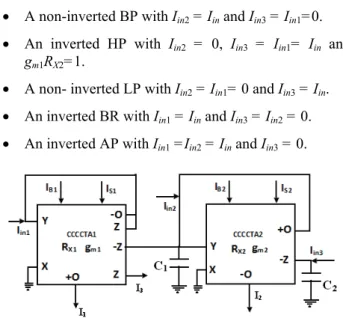
The proposed current-processing universal biquad filter circuit is shown in Fig. 2. It is based on two CCCCTAs and two grounded capacitors. Routine analysis of the proposed circuit yields the following current outputs.
1 2 2 3 2 1 1 2 ( ) ( ) in in in m m X I I C s I g I g R D s , (3)
1 2 2 3 2
2 2 2 ( ) ( ( )) ( ) in n in m m I I C s I g D s g I C s D s , (4)
1 1 2 2 2 1 2 2 3 1 2 2 3 [ ( ) ] ( ) in m X in m X in m X m I D s g R C s I g R C s I g R g I D s (5) where 2 1 2 2 1 2 2 2 ( ) X m X m D s s C C R sg R C g . (6) It can be seen from (5) that the proposed filter circuit can be used as three input single output (TISO) current-processing filter. The circuit realizes five standard filter functions at current output I3 which are as: A non-inverted BP with Iin2 = Iin and Iin3 = Iin1=0. An inverted HP with Iin2 = 0, Iin3 = Iin1= Iin and
gm1RX2=1.
A non- inverted LP with Iin2 = Iin1= 0 and Iin3 = Iin.
An inverted BR with Iin1 = Iin and Iin3 = Iin2 = 0. An inverted AP with Iin1 =Iin2 = Iin and Iin3 = 0.
Fig. 2. Proposed current-mode universal biquad filter.
In this design, it is to be noted that input current in-version is not required to realize the above standard filter functions. Only a simple current component matching condition is required to realize HP response. In addition, filter responses HP and AP requires additional copies of input current signals at the realizations. This solution re-quires an additional current follower to duplicate the input current signal. Moreover, the above proposed filter topol-ogy can also be used as single input three-output filter, if
Iin2 = Iin3 = 0 and by taking Iin1= Iinas single input current
terminal. From (3) - (5), the following current transfer functions can be obtained.
1 1 2 2 ( ) m X in g R C s I I D s , (7) 2 2 ( ) m in g I I D s , (8) 2 3 ( 1 2 2 2) ( ) X m in I C C R s g I D s . (9)
It can be seen from (7) - (9) that non-inverting BP, non-inverting LP and inverting BR filter responses are obtained from output currents I1, I2 and I3, respectively. Inverting HP and AP filter responses can be easily obtained from the currents IHP= I2 + I3 and IAP= I1 + I3, respectively.
The pole frequency (ωo), the quality factor (Q) and bandwidth (BW) ωo /Q of each filter can be expressed as
2 1 2 2 1 2 0 X m R C C g
, 2 1 2 2 2 1 1 1 X m m C R g C g Q , 1 1 0 C g Q BW
m . (10)Substituting intrinsic resistances and trans-conductance values as depicted in (2), the above equation yields 2 1 2 2 0 1 C C I I V B S T
, 2 1 2 2 1 2 C C I I I Q S B S . (11)In (11), by maintaining IB2= IS2= IS1, the pole fre-quency can be electronically adjusted by IB2 and IS2 without affecting the quality factor. It can also be noted that the quality factor can be electronically adjusted by IS1 without affecting the pole frequency. In addition, bandwidth (BW) of the system can be expressed
1 1 1 2 O S T I BW Q C V
. (12)Equation (12) shows that the BW can be linearly con-trolled by IS1. From (11) - (12), it is clear that parameters
ωo and Q can be simultaneously controlled electronically by adjusting bias currents, without disturbing the parameter
ωo/Q. Moreover, it can also be noted that high Q can be easily obtained using low value of IS1 and higher values of
IS2 and IB2.
3.
Non-ideal Analysis
Taking the non-idealities of CCCCTA into account, the relationship of the terminal voltages and currents can be rewritten as follow: Xi Xi Yi i Xi V I R V
, IZi piIXi, IZi
niIXi, Zi mi pi O g V I
, IO
nigmiVZi (13)where βi = (1 - εvi), εvi (|εvi| << 1) represents the voltage
tracking error from Y to X terminal. αpi = (1 - εpi), εpi
(|εpi| << 1) represents the current tracking error from X to +Z terminal. αni = (1 - εni), εni(|εni| << 1) represents the
current tracking error from X to -Z terminal. γpiand γni are
the trans-conductance inaccuracy factor from -Z to O and
-Z to -O terminal, respectively. The non-ideal analysis of the proposed filter in Fig. 2 yields the transfer functions as
1 2 1 1 2 3 1 2 2 1 1 1 2 [( ) ] ( ) p in n in in p p m p m X I I C s I g I g R D s
, (14) 1 2 1 1 2 2 2 3 2 1 2 2 2 2 2 2 [( ) ( ( ))] ( ) p in n in n in p p m n m I I C s I g D s g I C s D s
, (15) 1 1 1 1 2 2 2 1 1 2 2 3 1 1 2 2 2 3 [ ( ( ) ) ] ( ) in n n m X p n m X m in n m X in I D s g R C s g R g I g R C sI I D s (16) where 2 1 1 2 2 1 1 1 2 2 1 2 2 2 2 ( ) p X n n m X p p n m D s s C C R s g R C g (17)In this case, the ωo and Q are changed to
2 1 2 2 1 2 2 2 2 0 X m p n R C C g
, 2 1 2 2 2 1 2 2 2 1 1 1 1 1 X m n p n n p m C R g C g Q
. (18)The active and passive sensitivities of the proposed circuit are as 1, 2, 2 1 2 o X C C R S , 2, 2, 2, 2 1 2 o p n gm S , 1, 1, 1, 1, 1, 2, 2, ,1 1 0 o X p p n n p n m R g S , (19) 2, 2 1 2 X Q C R S , 2, 2, ,1 2, 2 1 2 n p m Q C g S , 1, 1, 1 1 n n m Q g S , 1 1 p Q S , 2, 1, 2, ,1 1 0 p p n X Q R S . (20)
From the above results, it can be found that all the sensitivities are low and within ‘unity’ in magnitude.
4.
Simulation Results
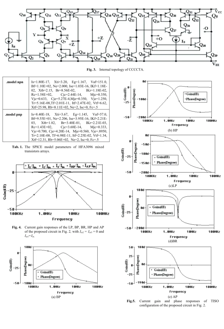
PSPICE simulations were carried out to demonstrate the workability of the proposed circuit. The CCCCTA was realized using BJT model as shown in Fig. 3, with the transistor model of HFA3096 mixed transistors arrays [11] and biased with ±1.75 V DC power supplies. The SPICE model parameters are given in Tab. 1. The circuit was designed for Q = 1 and fo = ωo/2π = 2.76 MHz. The active and passive components were chosen as IB1= IB2= 45 µA,
IS1= IS2= 180 µA, and C1= C2= 0.2 nF. Fig. 4 shows the simulated current gain responses of the LP, BP, BR, HP and AP of the proposed circuit of Fig. 2, with Iin2 = Iin3 = 0 and Iin1= Iin. Fig. 5 shows the simulated current gain and
phase responses of the BP, HP, LP, BR and AP of TISO configuration of the proposed circuit of Fig. 2. The simulated pole frequency was obtained as 2.62 MHz. The simulation results agree quite well with the theoretical analysis.
Fig. 3. Internal topology of CCCCTA.
.model npn Is=1.80E-17, Xti=3.20, Eg=1.167, Vaf=151.0,
Bf=1.10E+02, Ne=2.000, Ise=1.03E-16, IKf=1.18E-02, Xtb=2.15, Br=8.56E-IKf=1.18E-02, IKr=1.18E-IKf=1.18E-02, Rc=1.58E+02, Cjc=2.44E-14, Mjc=0.350, Vjc=0.633, Cje=5.27E-4,Mje=0.350, Vje=1.250, Tr=5.16E-08,Tf=2.01E-11, Itf=2.47E-02, Vtf=6.62, Xtf=25.98, Rb=8.11E+02, Ne=2, Isc=0, Fc=.5
.model pnp Is=8.40E-18, Xti=3.67, Eg=1.145, Vaf=57.0,
Bf=9.55E+01, Ne=2.206, Ise=3.95E-16, IKf=2.21E-03, Xtb=1.82, Br=3.40E-01, IKr=2.21E-IKf=2.21E-03, Rc=1.43E+02, Cjc=3.68E-14, Mjc=0.333, Vjc=0.700, Cje=4.20E-14, Mje=0.560, Vje=.8950, Tr=2.10E-08, Tf=6.98E-11, Itf=2.25E-02, Vtf=1.34, Xtf=12.31, Rb=5.06E+02, Ne=2, Isc=0, Fc=.5
Tab. 1. The SPICE model parameters of HFA3096 mixed
transistors arrays.
Fig. 4. Current gain responses of the LP, BP, BR, HP and AP
of the proposed circuit in Fig. 2, with Iin2 = Iin3 = 0 and
Iin1=Iin. (a) BP (b) HP (c)LP (d)BR (e) AP
Fig.5. Current gain and phase responses of TISO
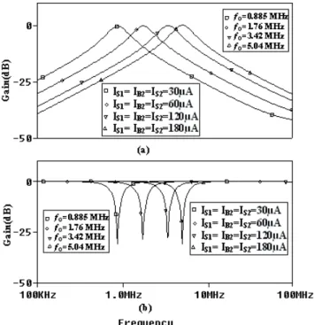
Fig. 6 shows magnitude responses of BP and BR (when Iin2 = Iin3 =0 and Iin1=Iin) functions where IB2, IS2 and IS1 were equally set and changed for several values, by keeping its ratio to be constant for constant Q (= 2). Other
parameters were chosen as IS2= 180 µA, and
C1=C2= 0.2 nF. The pole frequency (in Fig. 6) was found to vary as 0.885 MHz, 1.76 MHz, 3.42 MHz and 5.04 MHz for four values of IB2=IS2=IS1 as 30 µA, 60 µA, 120 µA and 180 µA, respectively, which shows that pole frequency can be electronically adjusted without affecting the quality factor. Fig. 7 shows the magnitude responses of BR and BP (when Iin2 = Iin3 = 0 and Iin1= Iin ) functions for different
values of IS1, by keeping IB1= IB2 = 45 µA, IS2= 180 µA, and
C1=C2= 0.2 nF. The quality factor was found to vary as 20, 12, 6 and 2.94, by keeping constant pole frequency as 2.62 MHz for four values of IS1 as 9 µA, 15 µA, 30 µA and 60 µA, respectively. This shows that the quality factor can be electronically adjusted without affecting pole frequency by input bias current IS1. The large signal behavior of the proposed circuit in Fig. 2 was also investigated by applying a 140 µA peak to peak input current sinusoidal signal at frequency 500 kHz. Fig. 8 shows the time domain sinusoi-dal current input and corresponding LP output signal of the proposed circuit of Fig. 2, with Iin2 = Iin3 = 0 and Iin1= Iin.
Fig. 6. (a) BR and (b) BP responses of the proposed filter for
different value of IB2= IS2= IS1 when Iin2 = Iin3 = 0 and
Iin1= Iin.
5.
Concluding Discussion
A current-processing current-controlled universal SITO/TISO biquad filter employing two CCCCTAs and two grounded capacitors is proposed. It may be noted that a cur-rent-processing circuit manipulates input signals as current(s) and provides output signal(s) also as current(s). Current
con-trol is a feature that allows the circuit parameters to be tuned through external current sources. The proposed circuit may require input current buffers, so as to meet the low input impedance requirements. Moreover, additional transistors need to be employed to obtain copies of input currents to be inserted at different nodes, wherever, input signal is to be applied at more than one node. The proposed filter possesses the following advantages: (i) realization of LP, HP, BP, BR and AP responses in current form with the single input three output or three input single output in the same configuration; (ii) the employment of minimum number of grounded capacitors; (iii) low active and passive sensitivity performance; (iv) electronic control of Q through single bias current without disturbing ω0; (v) availability of explicit current outputs (i.e. high impedance output nodes) without requiring any additional active elements; (vi) enjoys high-Q feasibility by adjusting the bias current(s). With above mentioned features, the proposed circuit is good for implementation as monolithic chip for portable electronic equipments. The proposed circuit is validated through simulation results which agree quite well with theoretical ones as expected, whereas the difference between them arises from non-idealities.
Fig. 7. (a)BR and (b) BP responses of the proposed filter for
different value of IS1 when Iin2 = Iin3 = 0 and Iin1 = Iin.
Fig. 8. Time domain input and LP output (I2) waveforms of
the proposed circuit in Fig .2 when Iin2 = Iin3 = 0 and
Acknowledgement
This work is a part of the first author’s Ph. D Thesis completed recently. The first author is thankful to Prof. D. S. Chauhan, Vice-Chancellor, Uttarakhand Univ., India for some motivating comments. The authors are thankful to anonymous reviewers for useful comments that helped to improve the paper. The authors are grateful to the Editor and the Associate Editor for recommending the paper.
References
[1] WILSON, B. Recent developments in current mode circuits. In Proceeding of IEE, Pt G., 1990, vol. 137, p. 63-67.
[2] TOUMAZOU, C., LIDGEY, F. J., HAIGH, D. G. Analogue IC Design: The Current-Mode Approach. London: Peter Peregrinus, 1990.
[3] SOLIMAN, A. M. New current-mode filters using current conveyors. Int’l Journal of Electronics and Communications (AEÜ), 1997, vol. 51, p. 275-278.
[4] SOLIMAN, A. M. Current mode universal filter. Electronics Letters, 1991, vol. 27, no. 18, p. 1614-1617.
[5] SOLIMAN, A. M. Current mode universal filters with grounded passive elements and using single output current conveyors. Journal of Active and Passive Electronic Devices, 2009, vol. 4, p. 55-62.
[6] WANG, C., ZHAO, Y., ZHANG, Q., DU, S. A new current-mode SIMO- type universal biquad employing multioutput current conveyors (MOCCII). Radioengineering, 2009, vol. 18, no. 1, p. 83-88.
[7] KESKIN, A. Ü., BIOLEK, D., HANCIOGLU, E., BIOLKOVA, V. Current-mode KHN filter employing current differencing transconductance amplifiers. Int’l Journal of Electronics and Communications (AEÜ), 2006, vol. 60, p. 443-446.
[8] FABRE, A., SAAID, O., WIEST, F., BOUCHERON, C. High frequency application based on a new current controlled conveyor. IEEE Transactions on Circuits and Systems-I: Fundamental Theory and Applications, 1996, vol. 43, no. 2, p. 82-91.
[9] KHAN, I. A., ZAIDI, M. H. Multifunction trans-linear-C current-mode filter. Int’l Journal of Electronics, 2000, vol. 87, p. 1047-1051.
[10] MAHESHWARI, S., KHAN, I. A. Novel cascadable current-mode translinear-C universal filter. Active and Passive Electronic Components, 2004, vol. 27, no. 4, p. 215-218.
[11] SENANI, R., SINGH, V. K., SINGH, A. K., BHASKAR, D. R. Novel electronically controllable current mode universal biquad filter. IEICE Electronics Express, 2004, vol. 1, no. 14, p. 410-415. [12] BIOLEK, D., BIOLKOVA, V. Universal biquads using CDTA
elements for cascade filter design. In Proceeding of the Int’l Multi Conference CSCC 2003. Corfu (Greece), 2003, p. 8-12.
[13] MINAEI, S., YUCE, E. Universal current-mode active-C filter employing only plus type current controlled current conveyors. Frequenz, 2006, vol. 60, p. 134–137.
[14] MINAEI, S., TURKOZ, S. Current-mode electronically tunable universal filter using only plus-type current controlled conveyors and grounded capacitors. ETRI Journal, 2004, vol. 26, no. 4, p. 292-296.
[15] KATOCH, T., TSUKUTANI, T., SUMI, Y., FUKUI, Y. Electronically tunable current-mode universal filter employing CCCIIs and grounded capacitors. In Proceeding of IEEE ISPACS, 2006, p. 107-110.
[16] KIRANON, W., KESORN, J., KAMPRASERT, N. Electronically tunable multi-function translinear-C filter and oscillators. Electronics Letters, 1997, vol. 33, no. 7, p. 573-574.
[17] SAGBAS, M., FIDABOYLU, K. Electronically tunable current-mode second order universal filter using minimum elements. Electronics Letters, 2004, vol. 40, p. 2-4.
[18] YUCE, E., MINAEI, S., CICEOGLU, O. Universal current-mode active-C filter employing minimum number of passive elements. Analog Integrated Circuits and Signal Processing, 2006, vol. 46, p. 169–171.
[19] MAHESHWARI, S., KHAN, I. A. High performance versatile translinear-C universal filter. Journal of Active and Passive Electronic Devices, 2005, vol. 1, p. 41-51.
[20] WANG, C., LIU, H., ZHAO, Y. A new current-mode current controlled universal filter based on CCCII (±). Circuits Systems and Signal Processing, 2008, vol. 27, p. 673-682.
[21] PANDEY, N., PAUL, S. K., JAIN, S. B. A new electronically tunable current-mode universal filter using MO-CCCII. Analog Integrated Circuits and Signal Processing, 2009, vol. 58, p. 171-178.
[22] BIOLEK, D., BIOLKOVA, V. CDTA-C current-mode universal 2nd order filter. In Proceeding of the 5th Int’l. Conference on Applied Informatics and Communications, 2003, p. 411-414. [23] ABUELMA'ATTI, M. T., Al-QAHTANI, M. L. Universal
current-controlled current-mode filter with three inputs and one output using current controlled conveyor. Active Passive Electronic Components, 1998, vol. 21, p. 33-41.
[24] CHANG, C. M. Universal active current filter using single second-generation current controlled conveyor. Circuits, Systems and Signal Processing, 2007, vol. 1,p. 194-198.
[25] TANGSRIRAT, W., SURAKAMPONTOR, W. High output impedance current-mode universal filter employing dual-output current-controlled conveyors and grounded capacitors. Int’l Journal of Electronics and communication (AEU), 2007, vol. 61, p. 127-131.
[26] CHEN, H. P., CHU, P. L. Versatile universal electronically tunable current-mode filter using CCCIIs. IEICE Electronics Express, 2009, vol. 6, no. 2, p. 122-128.
[27] WANG, H. Y., LEE, C. T. Versatile insensitive current-mode universal biquad implementation using current conveyors. IEEE Transactions on Circuits and Systems-II: Analog and Digital Signal Processing, 2001, vol. 48, p. 409-413.
[28] SIRIPRUCHYANUN, M., JAIKLA, W. Current controlled current conveyor transconductance amplifier (CCCCTA): A building block for analog signal processing. Electrical Engineering, 2008, vol. 90, p. 443-455.
[29] MANGKALAKECREE, S., DUANGMALAI, D., SIRIPRUCHY-ANUN, M. Current-mode KHN filter using single CC-CCTA. In The Seventh PSU Engineering Conference, 2009, p. 306-309. [30] SINGH, S. V., MAHESHWARI, S., CHAUHAN, D. S. Universal
current-controlled current-mode biquad filter employing MO-CCCCTAs and grounded capacitors. Circuits and Systems, 2010, vol. 1, p. 35-40.
[31] MAHESHWARI, S., SINGH, S. V., CHAUHAN, D. S. Electronically tunable low voltage mixed-mode universal biquad filter. IET Circuits, Devices and Systems, 2011, vol. 5, no. 3, p. 149-158. [32] SINGH, S. V., MAHESHWARI, S., CHAUHAN, D. S. Novel
Signal Processing, Lecture Notes in Electrical Engineering (LNEE). Springer, 2011, vol. 97, p. 735-742.
About Authors...
Sajai Vir SINGH was born in Agra, India. He received his B.E. degree (1998) in Electronics and Telecommunication from NIT Silchar, Assam (India), M.E. degree (2002) from MNIT Jaipur, Rajasthan (India) and Ph.D. degree (2011) from Uttarakhand Technical University. He is currently working as Assistant Professor in the Department of Elec-tronics and Communication Engineering of Jaypee Institute of Information Technology, Noida (India) and has been engaged in teaching and design of courses related to the design and synthesis of Analog and Digital Electronic Circuits. His research areas include Analog IC Circuits and
Filter design. He has published more than 20 research papers in various international journals/conferences. Sudhanshu MAHESHWARI was born in Aligarh, India. He obtained his B.Sc. (Engg.), M. Tech and Ph.D degrees from Aligarh Muslim University in 1992, 1999 and 2004 respectively. He is currently Associate Professor in the Department of Electronics Engineering of Aligarh Muslim University. He has been engaged in teaching and design of courses related to the design and synthesis of Analog Elec-tronic Circuits and Current-mode Circuits. His research areas include Analog Signal Processing and current-mode circuits. He has published more than 70 research papers, including around 55 international journal papers. He has supervised 2 Ph. Ds and more than 25 Master’s Disserta-tions and projects. He has been on the reviewer panel for several top ranked international journals.