Iowa State University Patents
Iowa State University Research Foundation, Inc.
5-7-2013
Logic element architecture for generic logic chains
in programmable devices
Arun K. Somani
Iowa State University
Follow this and additional works at:
http://lib.dr.iastate.edu/patents
Part of the
Electrical and Computer Engineering Commons
This Patent is brought to you for free and open access by the Iowa State University Research Foundation, Inc. at Iowa State University Digital Repository. It has been accepted for inclusion in Iowa State University Patents by an authorized administrator of Iowa State University Digital Repository. For more information, please [email protected].
Recommended Citation
Somani, Arun K., "Logic element architecture for generic logic chains in programmable devices" (2013).Iowa State University Patents. 70.
Logic element architecture for generic logic chains in programmable
devices
Abstract
A reconfigurable device includes an arrangement of a plurality of cells and routing resources for transmitting
signals between the cells. The plurality of cells comprises carry-select reuse cells, each of the carry-select reuse
cells configured to provide for performing non-arithmetic operations using a reuse arithmetic carry chain
interconnecting adjacent cells.
Disciplines
Electrical and Computer Engineering
US008438522B1
(12) United States Patent
(10) Patent N0.:
US 8,438,522 B1
Frederick et al.
(45) Date of Patent:
May 7, 2013
(54) LOGIC ELEMENTARCHITECTURE FOR 3,975,623 A 8/1976 Weinberger
GENERIC LOGIC CHAINS IN
2
1g;
?nelslld f
, , ue or
PROGRAMMABLE DEVICES 3,987,287 A 10/1976 CoX et al.
4,029,970 A 6/1977 H t l.
(75) Inventors: Michael T. Frederick, Colorado 4,032,394 A 6/1977 w?jjjgails
Springs, CO (US); Arun K. Somani, 4,034,356 A 7/1977 Howley et a1.
Ames IA (Us) 4,037,089 A 7/1977 Horninger
’ 4,041,459 A 8/1977 Horninger
. . . 4,051,358 A 9/1977 S h art
(73) Ass1gnee: Iowa State University Research
4,056,807 A
“H977 Tio‘glbei
Foundatlolla Inc-$11165, IA (US) 4,124,899 A 11/1978 Birkner etal.
4,140,921 A 2/1979 Balasubramanian et a1.
( * ) Notice: Subject to any disclaimer, the term ofthis 4,195,352 A 3/1980 Tu et al.
patent is extended or adjusted under 35
2
1?;
1531181179111? elt a1~
, , evine e a .
USC' 1540:’) by 904 days‘ 4,237,542 A 12/1980 Cukier
4,249,246 A 2/1981 Nanya et al.
(21) APP1- NO-I 12/237,076 4,293,783 A 10/1981 Patil
(22) Filed:
Sep. 24, 2008
(Continued)
(51) I Cl OTHER PUBLICATIONS
nt. .
G06F 17/50 (200601) Cong, Jason, “FlowMap: An Optimal Technology Mapping Algo
(52) U_s_ CL rithm for Delay Optimization in Lookup-Table Based FPGA
USPC ... .. 716/117; 716/ 121; 716/ 128 Designs”, IEEE Transactions on Computer-Aided Design Of Inte
(58) Field of Classi?cation Search ... .. 716/117, grated Circuits and Systems, V<>1~ 13,189 1, 1119 1994,1311 1-12~
716/ 121 128 -
’ C t d
See application ?le for complete search history. ( on lnue )
(56) References Cited Primary Examiner * Vuthe Siek
U.S. PATENT DOCUMENTS 3,230,355 A 1/1966 Chu
3,296,426 A 1/1967 Ball 3,313,926 A 4/1967 Minnick 3,400,379 A 9/1968 Harman 3,566,153 A 2/1971 Spencer, Jr. 3,702,985 A 11/1972 Proebsting 3,731,073 A 5/1973 Moylan 3,803,587 A 4/1974 Mead 3,816,725 A 6/1974 Greer 3,818,203 A 6/1974 Perlowskiet al. 3,849,638 A 11/1974 Greer 3,912,914 A 10/1975 Moylan 3,936,812 A 2/1976 Cox etal. 3,974,366 A 8/1976 Hebenstreit
i _ _ _ _ _ _ _ A _ __
Assistant Examiner * Mohammed Alam
(74) Attorney, Agent, or Firm * McKee, Voorhees & Sease, P.L.C.
(57)
ABSTRACT
A recon?gurable device includes an arrangement of a plural
ity of cells and routing resources for transmitting signals between the cells. The plurality of cells comprises carry
select reuse cells, each of the carry-select reuse cells con?g
ured to provide for performing non-arithmetic operations
using a reuse arithmetic carry chain interconnecting adjacent cells.
US 8,438,522 B1
Page 2
US. PATENT DOCUMENTS 5,075,576 A 12/1991 Cavlan 5,168,177 A 12/1992 Shankaretal. 413361601 A 6/1982 Tmka 5,204,555 A 4/1993 Grahametal. 4,348,736 A 9/1982 We1nberger 5210 448 A 5/1993 Takata
31332126 A
‘$32; got“ “all
5,212,652 A
5/1993 AgraWal etal.
413991516 A M983 Bfzgsetai 5,231,588 A 7/1993 AgraWal etal.
1 1 .9191 5,233,539 A 8/1993 AgraWal etal. 4,409,499 A 10/1983 Zap1sek et al. 5 302 865 A 4/l994 Steele et a1
414151818 A 11/1983 oga‘f’a etal' 53329460 A 7/1994 AgraWal etal.
414291238 A V1984 Hams?“ 5,359,536 A 10/1994 AgraWal etal.
4,433,331 A 2/1984 Kollar1tsch 5381551 A M995 Maedaetal
31232132 A @132: gqtze etal'
5,398,198 A
3/1995 Mahant-Shettietal.
1 1 “Ce 5,457,644 A 10/1995 McCollum
4,490,812 A 12/1984 Guterman 5 493 239 A 26996 Zlomick
4,495,590 A 1/1985 Mitchell, Jr. 5636439 A 66996 Steele etal
A128‘??? A
Ea? 6‘ a1~
5,640,106 A
6/1997 Erickson etal.
1 1 01 6 5,642,304 A 6/1997 Simpson
4,504,904 A 3/1985 Moore etal. 5687 325 A “H997 Chang
312821;? A
gull“
1
5,742,531 A
4/1998 Freidin etal.
1 1 New” 5,794,033 A 8/1998 Aldebertetal.
4,508,977 A 4/1985 Page etal. 5 805 477 A 96998 Pemer
3125123 A
jazz; iatake
5,844,829 A 12/1998 Freidin etal.
1 1 “n? 5,877,742 A 3/1999 Klink
4,516,040 A 5/1985 Zap1sek et al. 5 877 972 A 3/1999 Aoki et a1‘
3125218351; A
$322 gmlzletal'l
5,961,576 A 10/1999 Freidin etal.
415461273 A 166985 Ou° Set” 5,995,988 A 11/1999 Freidinetal.
1 1 mm 6,038,652 A 3/2000 Phillips etal.
4,551,814 A 11/1985 Moore etal. 6052 770 A 40000 Pant
4,551,815 A 11/1985 Moore etal. 6’065’028 A 50000 Dhong etal
A1231??? A
151322 ggllg 6‘ 5*
6,081,903 A
6/2000 Vorbach etal.
1 1 “*1 r' 6,119,048 A 9/2000 Kondo etal.
4,580,215 A 4/1986 Morton
. RE37,048 E 2/2001 McCollum
4,583,012 A 4/1986 Sm1th etal. 6188240 B1 2/2001 Nakaya
3123214933 A 13322 3mm
‘7:’?
6,209,077 B1
3/2001 Robertson etal.
416451953 A M987 Wamnanne a1 6,311,200 B1 10/2001 Hanrahanetal.
1 1 ‘mg 6,353,841 B1 3/2002 Marshall et al.
4,659,947 A 4/1987 Ogura etal. 6 404 227 B1 6/2002 Waggon
4,659,948 A 4/1987 Sunteretal. 6,449,628 B1 ’ ’ 9/2002 Wasson
4,660,171 A 4/1987 Mooreetal. - -
. 6,476,634 B1 11/2002 B1lsk1
4,661,922 A 4/1987 Th1erbach 6 539 477 B1 300% seawright
416751556 A 6/1987 Bazes 6,553,395 B2 4/2003 Marshall et al. 4,677,318 A 6/1987 Veenstra 6 573 749 B2 600% New et 31
416971105 A 9/1987 MOY 6,625,721 B1 9/2003 Chen
4,703,206 A 10/1987 Cavlan 6704 816 B1 3/2004 Burke
4,717,844 A 1/1988 Shimaetal. 6’732’l26 Bl 5/2004 Wang
A‘Zjgg‘fA
Z1322 Eiskett 1
6,754,686 B1
6/2004 Kaviani
417421252 A M988 Aungelti 6,873,181 B1* 3/2005 Pedersen ... .. 326/38
417451573 A
56988 Lggaiw
6,938,223 B2
8/2005 Boppanaetal.
1 1 e 6 7,007,264 B1 2/2006 Baxter
4,745,579 A 5/1988 Mead etal. 7047166 B2 5/2006 Dancea 417581746 A 7/1988 Blrkneretal' 7,164,288 B2 1/2007 Leijten-Nowak 4,758,747 A 7/1988 Young etal. 7193433 Bl 3/2007 Young
3132551???) A
$61.3?
7,196,541 B2
3/2007 NoWak-Leijten
417631626 A M988 Taiétamial 7,205,791 B1 4/2007 Leeetal.
1 1 .. ‘16 ~ 7,240,263 B2 7/2007 Bialas, Jr. et al.
4,772,811 A 9/1988 Fujloka et 311 7663 400 131* 2/2010 Plants “““““““““““““““ “ 326/38
4,774,421 A 9/1988 Hartmannetal. ’ ’ ,,
4786964 A 161988 Gah HI tal 2001/0049816 A1 12/2001 Rupp ... .. 716/16
1 1 r “n1 e ' 2006/0005090 A1* 1/2006 Langhammeretal. ... .. 714/725
417961229 A V1989 Greenlnetal' 2006/0091903 A1* 5/2006 Sood 326/40
4,815,022 A 3/1989 Glaeseretal. """"""""""""""" "
4,818,902 A 4/1989 Brockmann OTHER PUBLICATIONS 4,831,285 A 5/1989 Gaiser
4,831,573 A 5/1989 Norman Frederick, Michael T. et al., “Beyond the Arithmetic Constraint: 4339539 A 6/1989 Takata. et 31' Depth-Optimal Mapping of Logic Chains in LUT-based FPGAs”,
4,858,178 A 8/1989 Breunlnger ,
4,860,235 A 8/1989 Kondou et a1‘ FPGA 08 Feb. 24-26, 2008, Moneterey, CA, ACM 978-1-59593 4,870,302 A 9/1989 Freeman 934-0/08/02,PP~37-46~
4,876,466 A 10/ 1989 Kondou et al. Frederick, Michael T. et al., “Beyond the Arithmetic Constraint: 4,906,870 A 3/ 1990 Gongwer Depth-Optimal Mapping of Logic Chains in LUT-based FPGAs”, 4,918,641 A 4/1990 JigOUI et 61, Iowa State University, 2008 Dissertation, 167 pages.
4,931,671 A 6/1990 Agrawal Frederick, Michael T. et al., “Multi-Bit Carry Chains for High-Per
A
ghid‘gts it
formance Recon?gurable Fabrics”, Aug. 2006, Research paper par
5 5 10 e e a. . _
4,963,768 A
“V1990 Agrawalet a1‘
giligxglgpirgijnlzyeljssf g6ran;s :Snd the Jerry R. Junk1ns Endowment
4,965,472 A 10/1990 Anderson F d .k M. h 1Tty1 Plg‘N .thm . C Ch. f
A Burton et a1‘ re 6110 , 1C ae I .”et a ., on-ar1 6110 any a1ns Of
5,015,884 A 5/l991 Agrawal et a1‘ Recon?gurable Fabr1cs , IEEE 2007, #1-4244-1258-7/07, pp. 137 5,033,017 A 7/1991 Taniaietal. 143'
5,046,035 A 9/1991 Jigour etal.
US. Patent
50000
40000
30000
Frequency
20000
10000
May 7, 2013
Sheet 1 0f 8
- Frequency *Cumulative %
5 6 Fanout
FIG. 1
US 8,438,522 B1
10+ 100
90
US. Patent
May 7, 2013
Sheet 2 of8
US 8,438,522 B1
US. Patent
May 7, 2013
Sheet 3 of8
US 8,438,522 B1
US. Patent
May 7, 2013
Sheet 4 of8
US 8,438,522 B1
US. Patent
May 7, 2013
Sheet 5 0f8
US 8,438,522 B1
er,
get
FIG.
5
US. Patent
May 7, 2013
Sheet 6 of8
US 8,438,522 B1
@
After,
K=4
‘.5555 Before,
K=5
§
Forget,
K=5
[{5}]
Forget,
K=6
I\
After,
K=6
FIG.
6
1.1
US. Patent
May 7, 2013
Sheet 7 0f8
US 8,438,522 B1
5
Q
Before,
K=5
§
Forget,
K
I
After,
K
6
US. Patent
May 7, 2013
Sheet 8 of8
US 8,438,522 B1
02%
US 8,438,522 B1
1
LOGIC ELEMENT ARCHITECTURE FOR GENERIC LOGIC CHAINS IN PROGRAMMABLE DEVICES
GRANT REFERENCE
This invention Was made With government support under Grant No. CCF0311061 awarded by NSF. The government
has certain rights in the invention.
FIELD OF THE INVENTION
The present invention relates to recon?gurable fabrics, and
more particularly to carry chains used in recon?gurable fab rics.
BACKGROUND OF THE INVENTION
Carry chains in recon?gurable fabrics serve a very impor
tant, yet very speci?c purpose: to facilitate the e?icient imple
mentation of arithmetic functions. Carry chains alloW arith
metic functions to bypass the performance-costly general
routing array. However, if a carry chain is not used for an
arithmetic function, it becomes a super?uous adjacent cell
interconnection resource. There are several challenges to carry chain reuse for non-arithmetic chains, some architec tural, While others are based on tool support. What is needed is a modi?ed cell design that facilitates carry chain reuse.
Therefore, it is a primary object, feature, or advantage of
the present invention to improve over the state of the art. It is a further object, feature, or advantage of the present
invention to provide a modi?ed cell design that facilitates
carry chain reuse.
It is a still further object, feature, or advantage of the present invention to provide a means of improving design performance at a minimal cost.
Another object, feature, or advantage of the present inven
tion is to provide a means of improving designperformance in a manner Which is transparent to a designer.
One or more of these and/or other objects, features, or
advantages of the present invention Will become apparent
from the speci?cation and claims that folloW.
BRIEF SUMMARY OF THE INVENTION
Commercially available SRAM-based Field Program mable Gate Arrays (FPGAs) have gained traction in the engi
neering community as a highly ?exible and reusable embed
ded system design tool. FPGAs are also increasingly being
incorporated into production designs because their program
mability alloWs the addition of functionality, hardWare ?xes/
upgrades, or fault tolerance by Way of scrubbing or elimina
tion of faulty components. Due to their increasing inclusion in deployed systems, the need to fully utiliZe every architectural
resource is imperative so as to close the speed, area, and poWer consumption gap betWeen FPGAs and ASICs. The carry chain is one resource that has yet to be exploited to its
full capacity.
According to one aspect of the present invention, a recon ?gurable device includes an arrangement of a plurality of
cells and routing resources for transmitting signals betWeen the cells. The plurality of cells comprises carry-select reuse
cells, each of the carry-select reuse cells con?gured to pro
vide for performing non-arithmetic operations reusing an arithmetic carry chain interconnecting adjacent cells.
According to another aspect of the present invention, a
recon?gurable device including an arrangement of a plurality
20 25 30 35 40 45 50 55 60 65
2
of cells and routing resources for transmitting signals betWeen the cells. The plurality of cells comprises carry
select reuse cells, each of the carry-select reuse cells com
prising carry chain elements, look up tables, and sequential logic and Wherein the carry chain elements being con?gured
to provide for performing non-arithmetic operations reusing
an arithmetic carry chain interconnecting adjacent cells. According to another aspect of the present invention, a device has an architecture Which includes an arrangement of a plurality of cells and routing resources for transmitting
signals betWeen the cells. The plurality of cells includes
carry-select reuse cells, each of the carry-select reuse cells
comprising carry chain elements, look up tables, and sequen tial logic and Wherein the carry chain elements being con?g ured to provide for performing arithmetic operations and
being further con?gured for performing non-arithmetic
operations reusing an arithmetic carry chain interconnecting
adjacent cells.
BRIEF DESCRIPTION OF THE DRAWINGS
FIG. 1 illustrates distribution of net fanout.
FIG. 2 is a schematic of a carry-select traditional cell. FIG. 3 is a schematic of a carry-select reuse cell. FIG. 4 is schematic of a propagate-generate and carry
select addition logic.
FIG. 5 is a graph illustrating speedup of reuse ?oWs over
unmodi?ed ?oW for LUT of 4, 5, and 6 inputs.
FIG. 6 is a graph illustrating required FPGA channel Width of reuse ?oWs over unmodi?ed ?oW for LUT of 4, 5, and 6
inputs.
FIG. 7 is a graph illustrating total routed Wire length for
reuse ?oWs over unmodi?ed ?oW for LUT of 4, 5, and 6
inputs.
FIG. 8 is a schematic of a static mode output multiplexer.
DETAILED DESCRIPTION OF THE PREFERRED EMBODIMENT
Applications vary greatly from one to anotheriDSP applications are heavily arithmetic in nature, While many security algorithms are based on Boolean logic and use chains sparingly. For instance, an FFT is dominated by addition and
subtraction With 57.6 percent cells in chains, While DES3,
despite its complexity, predominately uses tabular look-ups
With only 0.8 percent chain cells. FIG. 1 shoWs an aggregate distribution of net fanout for a sampling of designs available at OpenCores [4]. Greater than 60 percent of the nets in the designs are a direct connection betWeen adjacent logic cells. Carry chain reuse is de?ned as a logic chain that has been
converted to use the arithmetic chain as a fast interconnect
structure betWeen adjacent cells. This forces these cells to be
placed next to each other during place and route (PNR), and
eliminates the need for that connection to traverse a con?g
urable routing structure. In general, this sampling of designs
seems to underutiliZe carry chains and could possibly bene?t
from their reuse.
This Work presents a modi?ed cell design that facilitates carry chain reuse. Post-technology map experiments shoW hoW reuse can bene?t all applications. The academic tool ?oW ofSIS [5], ChainMap [7], andVPR [2] is used to measure the effect of chain reuse on routing utiliZation and maximum
US 8,438,522 B1
3
A hardwired connection has been allocated in the Altera
Stratix architecture [1] that is capable of connecting LUTs
residing in the same block in a chain. This has the advantage
of avoiding general routing for Boolean chains of up to 10
LEs, the siZe of a block in the Stratix architecture. The LUT
chain is mapped by Quartus during PNR according to undis
closed metrics. Their functionality is similar to that of the
architecture proposed by this Work. The major difference
betWeen the approaches is that the LUT chain function can be replaced by a reusable carry chain. It is important to note that the Stratix II/ III architectures appear to have discontinued the LUT chain.
FPGAs use ripple-carry schemes, or slight variations thereof, for area ef?cient arithmetic computation. The Xilinx
Virtex series FPGAs are prime examples of highly-optimized ripple-carry use in commercial recon?gurable fabrics, using
their LUT logic to provide a propagate signal as the selection
input of a multiplexer choosing betWeen generate and cell carry-in (cin) [6], as shoWn in FIG. 4(a). The Altera Stratix
also uses ripple-carry as its base carry method, providing for
a 2-level chain for Stratix, and parallel ripple-chains With
LUT logic and dedicated full adders for the Stratix II [1]. The Stratix is based on the carry-select version of carry computa
tion. Each multiplexer in FIG. 4(b) chooses betWeen precom
puted sum (f) and carry out (c 1_ 1) based on the cell carry in
(cm). The carry-select scheme in Stratix directly facilitates
chain reuse. The carry in to each cell is directly mapped to the
selection input of a multiplexer choosing betWeen 2-LUTs.
Logically, the carry in serves as the 3rd input in a 3-LUT meaning that any LE con?gured as a 3 -LUT can use the native architecture to reuse the carry chain.
This invention is a Stratix-inspired reuse cell design for full-Width LUT output. A K-LUT describes the ability of an LUT to implement any K-input Boolean function. Thus, a
4-LUT implements all Boolean operations With 4 inputs. Traditional carry-select based LEs Working in random logic
(normal) mode implement one K-input, 1-output function,
and in arithmetic mode implement tWo independent (K—1) input, 1-output functions With K-l shared inputs. This inven tion supports the traditional normal and arithmetic modes, and in addition, provides the capability for a K-input, 2-out put function.
Tool support for carry chain synthesis is limited. Current softWare packages, such as Altera Quartus II and Xilinx ISE,
identify arithmetic carry chains through high-level HDL mac ros and primitives. The Xilinx V2P library guide denotes hoW
Wide homogeneous Boolean expressions (e. g. 16-inputAND)
can be formed using the carry chain, but synthesis does not identify and implement all such components, nor are the
primitives recogniZed by ISE v8.2. The only recourse is for the designer to implement such expressions using loW level
LUT and carry chain primitives. The most common academic
synthesis tool, SIS [5] doesn’t support arithmetic chains in its
internal representation.
FIG. 2 shoWs a rendition of the LE, similar to the stratix_ lcell LE primitive, dubbed the traditional cell that Will be used as the point of comparison to the reuse architecture depicted in FIG. 3. Several modi?cations have been made to the tradi tional cell that preserve its functionality and facilitate chain reuse. In the folloWing description, dataa' Will be used to refer
to the output of the XOR gate With inputs dataa and addsub,
While x Will be used to denote an ambiguous component or
signal.
In FIG. 3, a reuse cell 10 is shoWn. Data inputs datac 12, datab 14, dataa 16, datad 18, and cin 44 are shoWn. A mode
multiplexer 20 is provided Which receives input from datac 12
and may be used to set arithmetic or non-arithmetic mode. A
20 25 30 35 40 45 50 55 60 65
4
possible implementation of multiplexer 20 is shoWn in FIG. 8.
LUTs s l 22 and s0 24 are shoWn, and serve the role of com
puting the traditional arithmetic sum for the cases When the carry in 44 is a binary 1 or 0. Sum multiplexers 26, 28 are provided and multiplexer 4 is used to compute a sum. Carry
chain elements are also shoWn. LUTs c 1 30 and c0 32 serve the
role of computing the traditional arithmetic sum for the cases When the carry in cin 44 is a binary 1 or 0, and pass results
through multiplexers carl 34 and carO 36. A carry multiplexer
38 is also shoWn Which provides the carry output cout 40. In arithmetic mode, the traditional cell computes the sum of dataa' and datab using LUTs s1 and s0 and the sum multi
plexer, Whose result is passed through multiplexer 4. The
reuse cell on the other hand, passes each of the sum LUT values through a level of multiplexers and uses 42 (multiplexer 4) to compute sum. This is functionally equivalent
When the mode multiplexer is set in arithmetic mode (i.e.
static output). Similarly, carry computation is performed after
alloWing the LUT results to pass through multiplexers cart 34 and carO 36. Like the traditional design, carry computation is
completed once the carry in to the cell is available. The additional level of multiplexing in the reuse design institutes a delay on the carry once dataa' and datab 14 become avail able. Only the ?rst cell in a carry chain is affected because it is the only one dependent on the arrival of routing inputs. It is
assumed that in an synchronous design all routing inputs
become available at the same time, causing the carry chain to be the critical path of the circuit. All cells in the chain, With the
exception of the ?rst, have computed the carry for both cin
conditions before the arrival of cin to the carry multiplexer 38.
The sum computation expects identical latency, While the
carry latency only differs for the ?rst cell in a chain. Arith
metic mode preserves cout:f (dataa', datab, cin).
The normal operating mode of both cells is appreciably
different. In the traditional cell the mode multiplexer passes
routing input datad to multiplexer 4, While the reuse cell the mode multiplexer 20 passes datac to the car,C (34, 36) and
sum,C (26, 28) multiplexersia slight difference alloWing the
cout:f(dataa', datab, datac, cin) for non-arithmetic chains.
The combout function is computed similarly in both cell designs, the difference being that the LUT mask is rearranged
in the reuse cell. In arithmetic mode the carry and sum LUT
outputs must pass through the car,C (34, 36) and sum,C (26, 28) multiplexers Without performing a computation, Which
causes the middle nibbles of the 4-LUT mask to be inter changed in normal mode, as presented in the reuse mask in Table 3 and the traditional mask in Table 4. This is an innocu
ous change easily dealt With at the technology mapping stage.
In summary, no extra delays are introduced in the reuse cell for Boolean operations, the cout can accommodate a f (dataa', datab, datac, cin), and the combout can be the same function as the traditional cell of three general inputs and an input from
the 4:1 multiplexer. The 4:1 multiplexer options include an external data input, datax, cin, the register feedback of the
cell, regout, and addsub. The only functionality difference
betWeen the tWo cells is the value of datax (datad for reuse,
datac for traditional).
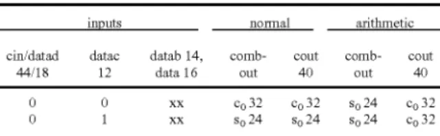
TABLE 3
inputs normal arithmetic
cin/datad datac datab 14, comb- cout comb- cout
44/18 12 data 16 out 40 out 40
US 8,438,522 B1
TABLE 3-continued
inputs normal arithmetic
cin/datad datac datab 14, comb- cout comb- cout
44/18 12 data 16 out 40 out 40
1 0 xx 0130 0130 s12 0130 1 1 xx s122 s122 s122 0130
TABLE 4
inputs normal arithmetic
datad cin/datac datab 14, comb- cout comb- cout
18 44/12 data 16 out 40 out 40
0 0 xx so 24 co 32 so 24 co 32
0 1 xx sl22 c130 sl22 0130
1 0 xx co 32 co 32 so 24 co 32
1 1 xx 0130 c130 s122 0130
Custom circuit layout and simulation results for the reuse and traditional cell in Table 1 indicate that couto, the initial cell in a chain, and the combout for all cells both suffer a 1.01x delay at 3.3 V 0.6 um process technology. Intermediate cells, countn_l ,1, experience no increase in delay. R:T gives the ratio of the reuse cell delay and area to that of the traditional cell.
TABLE 1
urn x urn couto coutmm combout
Reuse 97.95 x 82.35 6.04 ns 3.50 ns 5.94 ns
Trad 97.95 x 79.95 6.01 ns 3.49 ns 5.90 ns
R:T 1.03 1.01 1.00 1.01
A caveat of this Work is that the layout results obtained are
not necessarily representative of commercial cell implemen
tations. The assumptions are that the traditional and reuse cell
designs have been treated equally and that the performance of
the reuse cell relative to the traditional cell can be adequately
estimated by assessing an overall performance penalty When applicable. It is applicable during the ?rst cout computation in
a chain and the combout of every cell in the design. In the overall cell layout, area is dominated by the 20 SRAM con
?guration bits, D ?ip-?op, pass transistor 4-LUT structure,
and the output control. In this context, the tWo additional 2:1 pass transistor multiplexers of the reuse cell yield a 1 .03x area increase.
Combining this invention With a generic logic chain
assignment method such as that presented in [7] alloWs FPGA LEs to have equal access to the fast chain resources ubiqui
tous in today’s commercial architectures. In experiments pre sented in [8], HDL chains are preserved through synthesis
and technology mapping (after, normal), through only syn
thesis (before), and not preserved (forget). Each circuit is
mapped to an FPGA With the minimum amount of component
and routing resources required for implementation. LUT
Widths of 4, 5, and 6 inputs are tested.
Speedup is de?ned as the ratio of the critical path delay of
the reuse cell to that of traditional cell; higher speedup indi cates a performance increase for the reuse cell. The effect of this invention on the average speedup of circuits, as depicted in FIG. 5, is approximately 1.05x, With a minimum of 0.73x and maximum of 1 .45x Witnessed. Increasing the Width of the
LUT, the current trend in commercial architectures, generally yields higher performance increases for the reuse cell.
20 25 30 35 40 45 55 60 65
6
The change in channel Width is de?ned as the ratio of the channel Width of the reuse cell to that of the traditional cell; higher channel Width ratio indicates a performance decrease for the reuse cell. FIG. 6 indicates that an increase in speedup for the reuse cell often comes at the cost of an increase in the
FPGAs required channel Width. The average change in chan
nel Width is a 1.05x increase With a minimum of 0.7x and maximum of 1.4x observed. This indicates that an increase in the routing resources of an FPGA is required if performance increases are to be reaped by the invention.
The change in total routed Wire length is de?ned as the ratio of the total routed Wire length of the reuse cell to that of the
traditional cell; higher total routed Wire length ratio indicates
a performance decrease for the reuse cell. FIG. 7 indicates that an increase in speedup for the reuse cell often comes at the cost of a small increase in the FPGAs required total routed
Wire length. The average change in total Wire is neutral, at
1.0x, With a minimum of 0.78x and maximum of 1.35x observed. This indicates that this invention more completely uses the routing resources offered by an FPGA.
The present invention provides a Way to reuse arithmetic carry chains in FPGAs to offer bene?ts to non-arithmetic operations. A modi?ed cell architecture based on the carry
select ripple chain is presented and shoWn to increase delay through the cell by 1.01x and increase utilization by 1.03x. Traditional functionality is preserved at minimum cost, and
the added delay in the carry chain is only an issue at the ?rst cell in a chain. The result is an architecture that is able to pass its full K-LUT value along the carry chain. To study the effect of chain reuse for a commercial design tool and architecture,
the chain assignment technique presented in [7] and the rest of the academic design flow were used by [8] for four separate strategies of treating HDL based arithmetic chains. Speedup, channel Width ratio, and total routed Wire length ratio results
indicate that circuits can bene?t from this invention’s inclu sion in commercial FPGA architectures. While some circuits
often simultaneously increase performance and decrease
routing consumption, others may do quite the opposite. The
success of the invention in a particular application may depend on the characteristics exhibited by the design, such as number of arithmetic chain cells, number of cells in the design, the average fanout of each net, and, mo st importantly,
the chain assignment algorithm chosen.
Logic chains may use the carry chain as a 0 delay intercon nection structure regardless of HDL macros. The post-place and route experiments shoW chain reuse has great potential based in this invention’s ability to obviate the difference betWeen arithmetic and non-arithmetic chains. At a time When FPGA vendors are increasing the Width of the LUT from 4 to 5 to 6 inputs and beyond, this invention provides a basis to support chain operations that exceed the minimal requirements of simple arithmetic chains in an e?icient and minimally invasive manner. Such support combats the
underutiliZation caused by 3-input arithmetic operations
using a 6-input LUT.
Carry chain reuse can be a valuable addition to recon?g urable architectures and their design How. Results indicate that even With naive algorithms, a design/algorithm pair can be found that can potentially increase maximum clock fre quency, With an observed maximum of 1.45x, and decrease
routing consumption, With an observed minimum of 0.7x, for the presented circuits. It is another step toWard fully hamess
ing the complete computing capacity of FPGAs.
US 8,438,522 B1
7
REFERENCES
All references listed are herein incorporated by reference
in their entirety.
[1] Altera. Stratix Series User Guides. http://WWW.altera.
com.
[2] V. BetZ, J. Rose, andA. Marquardt. Architecture and CAD
for Deep-Submicron FPGAs. KluWer, NorWell, Mass.,
1999.
[3] S. Malhotra, T. Borer, D. Singh, and S. BroWn. The quar tus university interface program: enabling advanced fpga research. In Proceedings of the 2004 IEEE Intl Conference on Field-Programmable Technology, pages 225-230,
December 2004.
[4] OpenCores. http://WWW.opencores.org/, 2007.
[5] E. Sentovich et al. Sis: A system for sequential circuit
synthesis. Technical Report UCB/ERL M92/41, EECS
Department, University of California, Berkeley, 1992.
[6] Xilinx. I/irtex Series User Guides. http://WWW.XilinX.com
[7] M. T. Frederick and A. K. Somani. Beyond the arithmetic
constraint: depth-optimal mapping of logic chains in LUT based FPGAs. In Proceedings of the Sixteenth ACM/
SIGDA Int ’l Symposium on Field-Programmable Gate
Arrays, pages 37{46, February 2008.
[8] M. T. Frederick. Beyond the arithmetic constraint: depth
optimal mapping of logic chains in recon?gurable fabrics.
Iowa State University Dissertation, May 2008.
What is claimed is:
1. A recon?gurable device including: an arrangement of a
plurality of cells and routing resources for transmitting sig
nals betWeen the cells, Wherein the plurality of cells com
prises carry-select reuse cells, each of the carry-select reuse cells con?gured to provide for performing non-arithmetic
operations using a reuse arithmetic carry chain interconnect
ing adjacent cells When a non-arithmetic mode input is
received to provide a non-arithmetic mode and further con
?gured to perform arithmetic operations using the reuse arith
metic carry chain When an arithmetic mode input is received to provide an arithmetic mode, Wherein in the arithmetic
mode, the carry-select reuse cells provide for tWo indepen
dent (K-l) input, 1-output functions With K—1 shared inputs;
Wherein in the non-arithmetic mode, the carry-select reuse
cells provide for one K-input 1-output function;
Wherein the carry-select reuse cells further provide for a
K-input, 2-output function; Wherein K is a number of
inputs of a lookup table associated With the carry select
reuse cells.
2. The recon?gurable device of claim 1 Wherein the recon
?gurable device is a ?eld programmable gate array (FPGA).
3. The recon?gurable device of claim 1 Wherein the reuse arithmetic carry chain provides a carry output, the carry out put providing an output of a function de?ned by the carry select reuse cells for non-arithmetic chains.
4. The recon?gurable device of claim 1 Wherein each of the
carry-select reuse cells comprises carry chain elements, look up tables, and sequential logic con?gured to alloW the reuse
arithmetic carry chain to be used for arithmetic or non-arith
metic operations.
5. The recon?gurable device of claim 1 Wherein the
arrangement being at least partially determined by applying
an algorithm for creating non-arithmetic chains.
6. A recon?gurable device including: an arrangement of a
plurality of cells and routing resources for transmitting sig
20 25 30 35 40 45 50 55 60
8
nals betWeen the cells, Wherein the plurality of cells com
prises carry-select reuse cells, each of the carry-select reuse cells comprising carry chain elements, look up tables, and sequential logic and Wherein the carry chain elements being con?gured to provide for performing non-arithmetic opera
tions using a reuse arithmetic carry chain interconnecting adjacent cells When a non-arithmetic mode input is received to provide a non-arithmetic mode and further con?gured to
perform arithmetic operations using the carry chain elements
When an arithmetic mode input is received to provide an
arithmetic mode, Wherein in the arithmetic mode, the carry select reuse cells provide for tWo independent (K-l) input, 1-output functions With K—1 shared inputs;
Wherein in the non-arithmetic mode, the carry-select reuse
cells provide for one K-input, 1-output function;
Wherein the carry-select reuse cells further provide for a
K-input, 2-output function; Wherein K is a number of
inputs of a lookup table associated With the carry select
reuse cells.
7. The recon?gurable device of claim 6 Wherein the recon
?gurable device is a ?eld programmable gate array (FPGA).
8. The recon?gurable device of claim 6 Wherein the carry chain elements provide a carry output, the carry output pro viding an output of a function de?ned by the carry-select reuse cells for non-arithmetic chains.
9. The recon?gurable device of claim 6 Wherein the
arrangement being at least partially determined by applying
an algorithm for creating non-arithmetic chains.
10. A device having an architecture comprising: an arrangement of a plurality of cells and routing resources for
transmitting signals betWeen the cells, Wherein the plurality
of cells comprises carry-select reuse cells, each of the carry
select reuse cells comprising carry chain elements, look up
tables, and sequential logic and Wherein the carry chain ele ments being con?gured to provide for performing arithmetic
operations When an arithmetic mode input is received to pro vide a non-arithmetic mode and being further con?gured for performing non-arithmetic operations using a reuse arith metic carry chain interconnecting adjacent cells When a non arithmetic mode input is received to provide an arithmetic
mode, Wherein in the arithmetic mode, the carry-select reuse
cells provide for tWo independent (K-l) input, 1-output func
tions With K—1 shared inputs;
Wherein in the non-arithmetic mode, the carry-select reuse
cells provide for one K-input, 1-output function;
Wherein the carry-select reuse cells further provide for a
K-input, 2-output function; Wherein K is a number of
inputs of a lookup table associated With the carry select
reuse cells.
11. The device of claim 10 Wherein the device is a ?eld
programmable gate array (FPGA).
12. The device of claim 10 Wherein the carry chain ele ments provide a carry output, the carry output providing an output of a function de?ned by the carry-select reuse cells for non-arithmetic chains.
13. The device of claim 10, Wherein in the arithmetic mode, a sum is computed using sum lookup tables, values from the
sum lookup tables passing through a level of multiplexers and
then an additional multiplexer to compute a sum.
14. The device of claim 13, Wherein carry computation is
performed after alloWing lookup table results to pass through
an additional level of multiplexing.