Plasmonics: Numerical Methods and Device Applications
Thesis by
Luke A. Sweatlock
In Partial Fulfillment of the Requirements
for the Degree of
Doctor of Philosophy
California Institute of Technology
Pasadena, California
2008
ii
c 2008 Luke A. Sweatlock
iii
iv
Acknowledgements
It is my pleasure to acknowledge the many people who have supported me during my stay at Caltech.
First of all I would like to thank my advisor Harry Atwater, for providing the opportunity to study in an
exciting field, and for being a constant source of research inspiration and of infectious enthusiasm. Thanks
also to Albert Polman for making me feel welcome as a visitor, and for many years of insightful advice.
During my time in the Atwater group I was lucky to be surrounded by a great group of fellow students
who always made the lab an enjoyable and enlightening environment. I owe a great debt of gratitude to all
of my colleagues and collaborators. In particular, I want to thank my mentor Stefan Maier, and my regular
co-authors Joan Penninkhof and Jennifer Dionne for their absolutely invaluable support.
I would also like to acknowledge the generous funding for this work, mainly provided by the Air Force
Office of Scientific Research, and by the National Science Foundation via the Center for Science and
Engi-neering of Materials at Caltech.
Finally, thanks to all my friends and family, and especially to Sarah, for making this journey possible.
Luke Sweatlock
May 2008
v
Abstract
Plasmonics is a rapidly evolving subfield of nanophotonics that deals with the interaction of light with surface
plasmons, which are the collective charge oscillations that occur at the interface between conductive and
dielectric materials. Plasmonics meet a demand for optical interconnects which are small enough to coexist
with nanoscale electronic circuits. Emerging technologies include very small, low-power active devices
such as electrooptic or all-optical modulators. Passive plasmonic devices, or “optical antennas,” are being
used to enhance the performance of emitters and detectors, and to harvest sunlight for photovoltaics. This
manuscript focuses on the process of developing novel plasmonic devices from concept to prototype, with
specific emphasis on synthesizing data from numerical simulation and from empirical characterization into
an accurate, predictive understanding of nanoscale optical phenomena.
The first part of the thesis outlines the development of numerical methods. In the case of resonant
nanos-tructures such as small metal particles, the principal technique employed is impulse excitation ringdown
spectroscopy. This method allows the critical advantage of generating broadband spectra from a single
time-domain simulation. For analysis of plasmonic waveguides, Fourier-space analysis is used to reveal the
dis-persion properties of supported modes, and to perform filtering in the wavevector domain or “k-space”. The
remainder of the thesis deals with the design and characterization of plasmonic devices, with the broad and
Contents
Acknowledgements iv
Abstract v
List of Figures x
List of Tables xiii
List of Publications xiv
1 Introduction 1
1.1 Motivation . . . 1
1.2 Optical Constants . . . 3
1.2.1 Physical origin of the Lorentz model . . . 5
1.2.2 Multi-oscillator Lorentz-Drude model . . . 6
1.2.3 Extended Drude model . . . 7
1.2.4 Debye model . . . 7
1.3 Resonant Plasmonic Properties of Metal Particles . . . 8
1.3.1 Small metal particles in the quasistatic approximation . . . 8
1.3.2 Introduction to non-quasistatic particles . . . 10
1.4 Surface Plasmons on Metallic Films . . . 11
1.5 Scope of this Thesis . . . 17
1.5.1 Part I: Numerical Analysis Methods . . . 17
1.5.2 Part II: Resonant Plasmonic Nanostructures . . . 18
I
Numerical Analysis Methods
20
2 Impulse Excitation Analysis of Resonators 21
2.1 Introduction . . . 21
2.2 Impulse Excitation, Resonant Ringdown Method . . . 22
2.3 Selection of Individual Modes by On-Resonance Excitation . . . 24
3 Fourier Mode Spectrum Analysis 30 3.1 Introduction . . . 30
3.2 Preprocessing Time-Domain Data for Mode Spectrum Analysis . . . 31
3.2.1 Construction of time-harmonic fields . . . 31
3.2.2 Scattering via linear field subtraction . . . 31
3.3 Fourier Mode Spectral Analysis Method . . . 34
3.4 Application of FMSA to Characterization of Groove In-coupling . . . 38
II
Resonant Plasmonic Nanostructures
40
4 Mega-Electron-Volt Ion Beam Induced Anisotropic Plasmon Resonance of Silver Nanocrystals in Glass 41 4.1 Introduction . . . 414.2 Method . . . 42
4.3 Results . . . 43
4.4 Conclusion . . . 47
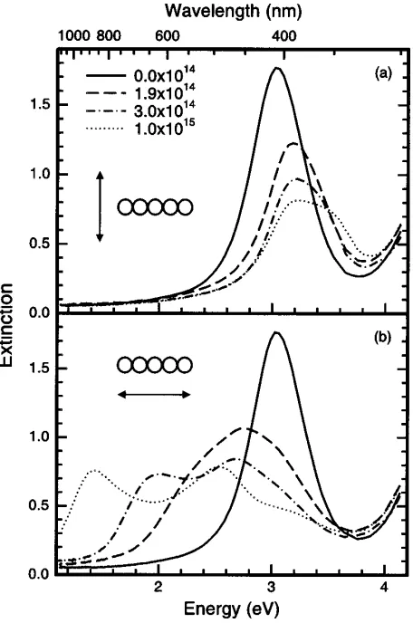
5 Highly Confined Electromagnetic Fields in Arrays of Strongly Coupled Silver Nanoparticles 48 5.1 Introduction . . . 49
5.2 Nanoparticle Array Fabrication . . . 50
5.3 Optical Absorption Spectroscopy . . . 52
5.5 Results and Discussion . . . 56
5.6 Conclusion . . . 62
6 Plasmon-Enhanced Photoluminescence of Silicon Quantum Dots: Simulation and Experiment 64 6.1 Introduction . . . 65
6.1.1 Field enhancements and spontaneous emission . . . 66
6.2 Experimental Section . . . 67
6.3 Results and Discussion . . . 71
6.4 Conclusions . . . 78
7 Plasmonic Modes of Annular Nanoresonators Imaged by Spectrally Resolved Cathodolumines-cence 80 7.1 Introduction . . . 80
7.2 Results . . . 80
7.3 Conclusion . . . 91
III
Guided-wave Plasmonics
92
8 Plasmon Slot Waveguides: Towards Chip-Scale Propagation with Subwavelength-Scale Local-ization 93 8.1 Introduction . . . 948.2 Mode Propagation and Skin Depth . . . 98
8.3 Conclusions . . . 100
9 Plasmonic Waveguide Cavity and Incoupling Analysis 102 9.1 Incoupling into Metal/Insulator/Metal Structures . . . 102
9.2 Multilayer MIM structures with vias . . . 106
IV
Appendices
111
A Microwave Antenna-Waveguide Subwavelength Interferometer 112
A.1 Abstract . . . 112
A.2 Introduction . . . 112
A.3 Apparatus . . . 113
A.4 Design Considerations . . . 114
A.5 Demonstration of Concept . . . 116
A.6 Experimental Results . . . 116
A.7 Simulation Results . . . 117
A.8 Conclusions . . . 119
B Optical Properties of Materials 120 B.1 Drude Model Au and Ag . . . 120
B.2 Lorentz-Drude Model Metals . . . 123
List of Figures
1.1 Surface plasmon dispersion relation for an Ag/SiO2interface . . . 12
1.2 Surface plasmon propagation length for an Ag/SiO2interface . . . 15
1.3 Surface plasmon electric field penetration depth in Ag and SiO2 . . . 16
2.1 Impulse excitation ringdown spectroscopy of a metallic shell . . . 23
2.2 Schematic of cylindrical Si/Ag core-shell particle . . . 25
2.3 Multimode spectral characterization of a cylindrical Si/Ag core-shell resonator, and subsequent isolation of a single resonance . . . 26
2.4 Mode selection by controlling symmetry of impulse function . . . 27
2.5 Characterization of selected modes by field divergence . . . 27
3.1 Determination of scattered fields by subtraction . . . 32
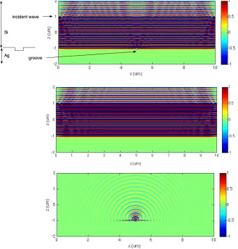
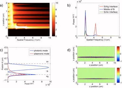
3.2 Scattered power versus angle from subwavelength scattering centers in a Si/Ag surface . . . . 34
3.3 SimulatedHypropagation in a multimode Ag/nitride/Ag waveguide with 500 nm thick core. Several plasmonic and conventional guided modes are present. . . 35
3.4 Fourier space power spectral maps of a Ag/nitride/Ag waveguide . . . 36
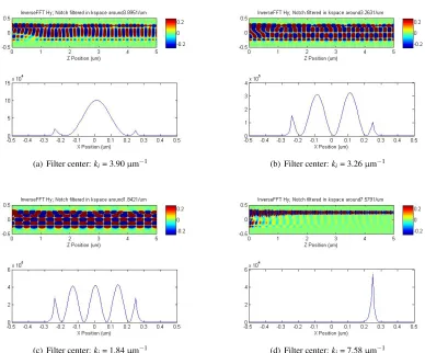
3.5 Mode isolation by Fourier space filtering. . . 37
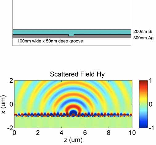
3.6 Scattering from a subwavelength groove in a thin-film-Si on Ag interface. . . 38
3.7 Fourier space analysis of scattering from a subwavelength groove in a thin-film-Si on Ag surface. 39 4.1 Optical extinction spectra of ion-irradiated Ag nanocrystals in glass. . . 44
4.2 TEM images of Ag nanocrystal alignment after Si irradiation. . . 45
4.3 Optical extinction spectra vs. Si-irradiation fluence. . . 46
5.1 Plan-view TEM images of arrays of small Ag nanoparticles in glass . . . 51
5.2 Measured optical extinction resonance peak energy vs. fluence of 30 MeV Si ions. . . 52
5.4 2D images of simulated resonant field intensity in arrays of four closely spaced Ag nanoparticles 58
5.5 E-field intensity on a line through the dielectric gap at the center of closely spaced Ag
nanopar-ticle arrays . . . 59
5.6 2D E-field maps show both “wire-like” and “particle-like” modes in arrays with touching Ag nanoparticles . . . 60
5.7 Simulated collective resonance frequency for arrays of 10 nm Ag particles, with various spac-ing and total array length . . . 61
6.1 Schematic, and simulated field intensity maps for arrays of np-Ag cylinders . . . 68
6.2 Collective plasmon resonance for np-Ag array determined via impulse ringdown simulation . 70 6.3 Computed field intensity enhancement in a plane 10 nm below np-Ag array vs. incident angle 71 6.4 Spectra of calculated absorption versus experimental transmission for arrays with various np-Au diameter . . . 72
6.5 Resonant peak wavelengths determined by computation vs. experiment for arrays with various np-Au diameter . . . 73
6.6 Computed field intensity enhancement vs. experimentally determined photoluminescence (PL) enhancement . . . 75
6.7 Computed field intensity enhancement in the nc-Si plane for arrays of np-Ag withd=50 or 100nm, and varying pitch,p . . . 76
6.8 In-plane field intensity enhancement as a function of depth from the base of the np-Ag array for various np-Ag diameter,d . . . 78
7.1 Panchromatic CL imaging of Ag annular nanoresonators . . . 85
7.2 Simulated modes in Ag annular nanoresonator . . . 86
7.3 Spectrally resolved imaging of plasmonic modes in an Ag annular nanresontator. . . 88
7.4 Imaging modes in a single-crystal Au nanoresonator . . . 90
8.1 Dispersion relations for MIM planar waveguides with an SiO2core and Ag cladding . . . 96
8.3 MIM (Ag/SiO2/Ag) TM-polarized propagation and skin depth . . . 99
9.1 Illustrated survey of simulated geometries for coupling into Ag/Si/Ag plasmonic waveguide . 105 9.2 Stack of two buried MIM waveguides connected by single via . . . 107
9.3 Schematic view of multi-layer plasmonic interferometer simulation. . . 108
9.4 Simulated performance of a switchable, multilayer plasmonic interferometer. . . 109
A.1 Microwave antenna waveguide test station. . . 113
A.2 Symmetric Yagi waveguide modulator schematic. . . 114
A.3 Interference at right angle intersection . . . 116
A.4 Yagi T modulator transmitted power, experimental data. . . 117
A.5 Yagi T modulator simulation . . . 118
A.6 Comparison of experimental modulation with simulation . . . 119
B.1 Drude model permittivity of Au . . . 121
B.2 Drude model permittivity of Ag . . . 122
List of Tables
9.1 Power incoupled to Ag/Si/Ag plasmonic waveguide from free space Gaussian beams in endfire
or slit configuration, or from Si core dielectric waveguide. . . 104
B.1 Optical permittivity of transparent dielectrics . . . 120
B.2 Drude model permittivity of metals . . . 121
B.3 Gold (Au) Lorentz-Drude model parameters . . . 123
B.4 Silver (Ag) Lorentz-Drude model parameters . . . 123
B.5 Copper (Cu) Lorentz-Drude model parameters . . . 124
B.6 Aluminum (Al) Lorentz-Drude model parameters . . . 124
List of Publications
Portions of this thesis have been drawn from the following sources:
Articles
“Optical cavity modes in gold shell colloids,” J. J. Penninkhof, L. A. Sweatlock, H. A. Atwater, A. Moroz,
A. van Blaaderen, and A. Polman.Journal of Applied Physics, (In press).
“Plasmonic Modes of Annular Nanoresonators Imaged by Spectrally-resolved Cathodoluminescence,” C. E. Hofmann, E. J. Vesseur, L. A. Sweatlock, H. J. Lezec, F. J. Garcia de Abajo, A. Polman, and H. A. Atwater.
Nano Letters,73612 (2007).
“Plasmon-enhanced photoluminescence of Si quantum dots: Simulation and experiment,” J. S. Biteen, L. A. Sweatlock,
H. Mertens, N. S. Lewis, H. A. Atwater, and A. Polman.Journal of Physical Chemistry C,11113372-13377 (2007).
“Plasmon slot waveguides: Towards chip-scale propagation with subwavelength-scale localization,” J. A. Dionne, and L. A. Sweatlock, H. A. Atwater, and A. Polman.Physical Review B,73035407 (2006).
“Planar metal plasmon waveguides: frequency-dependent dispersion, propagation, localization, and loss
be-yond the free electron model,” J. A. Dionne, and L. A. Sweatlock, H. A. Atwater, and A. Polman. Physical Review B,72075405 (2005).
“Highly confined electromagnetic fields in arrays of strongly coupled Ag nanoparticles,” L. A. Sweatlock, S. A. Maier, H. A. Atwater, J. J. Penninkhof, and A. Polman.Physical Review B,71235408 (2005).
“Mega-electron-volt ion beam induced anisotropic plasmon resonance of silver nanocrystals in glass,” J. J.
Proceedings, Books Chapters, and Manuscripts
“All-optical Plasmonic Modulators and Interconnects,” D. Pacifici, H. J. Lezec, L. A. Sweatlock, C. de Ruiter,
V. E. Ferry, and H. A. Atwater. In S. I. Bozhevolnyi, editor,Plasmonic Nanoguides and Circuits(In press).
“Universal optical transmission features in periodic and quasiperiodic hole arrays,” D. Pacifici, H. J. Lezec, L. A. Sweatlock, R. J. Walters, and H. A. Atwater. (Submitted).
“PlasMOStor: a metal-oxide-silicon field effect plasmonic modulator,” J. A. Dionne, K. A. Diest, L. A. Sweatlock, and H. A. Atwater. (Submitted).
“Subwavelength-scale Plasmon Waveguides,” H. A. Atwater, J. A. Dionne, and L. A. Sweatlock. In M. L.
Brongersma and P. G. Kik, editors,Surface Plasmon Photonics, pages 87–104. Dordrecht, NL: Springer.
“The new ‘p-nJunction’: Plasmonics Enables Photonic Access to the Nanoworld,” H. A. Atwater, S. Maier, A. Polman, J. A. Dionne, and L. A. Sweatlock.Materials Research Society Bulletin,30, 385 (2005).
Chapter 1
Introduction
1.1
Motivation
Plasmonics is a rapidly evolving subfield of nanophotonics that deals with the interaction of light with surface
plasmons, which are the collective charge oscillations that occur at the interface between conductive and
dielectric materials. Resonators made from metal nanostructures can confine concentrated optical energy to
tiny regions of space, much smaller than a wavelength of light in free space. Likewise many exotic effects
can be achieved with metallic waveguides, such as guiding light at optical frequencies with a tiny,
X-ray-like wavelength; or even with a negative effective optical index. The possible applications of plasmonics
abound in any field which would benefit from enhanced control of photons; from beamsteering to
single-molecule biodetection. Even such extraordinary technologies as micro-targeted infrared cancer therapy and
“invisibility cloaks” are on the horizon.
Our work has focused on the development of applications for optoelectronics. In this area, plasmonics
meet a demand for optical interconnects which are small enough to coexist with nanoscale electronic
cir-cuits. Emerging technologies include very small, low-power active devices such as electrooptic or all-optical
modulators. Passive plasmonic devices, or “optical antennas,” are being used to enhance the performance
of emitters and detectors, and to harvest sunlight for photovoltaics. This thesis will focus on the process of
developing novel plasmonic devices from concept to prototype, with specific emphasis on synthesizing data
from numerical simulation and from empirical characterization into an accurate, predictive understanding of
The strong interaction between microscopic metal particles and light has been exploited for thousands
of years, most recognizably in the art of creating brightly colored stained-glass window panels by annealing
metallic salts in otherwise transparent glass. Many dozens of practical recipes for this ancient
“nanofabri-cation” technique survive from as early as the 8th century A.D. (The Book of the Hidden Pearl, Jabir ibn
Hayyan). Roman artisans also produced remarkable dichroic glass artworks, although only one piece
sur-vives intact, the “Lycurgus Cup” dated 4th century A.D. Viewed normally by reflected light the surface is
opaque olive green, but when backlit the cup is a brilliant translucent red. This unusual effect is thematic to
the depicted scene, which captures Lycurgus at the moment he is dragged below to the underworld by a vine.
The microscopic origin of the optical dichroism is, in fact, the inclusion of gold and silver particles which are
about 60 nm in diameter, and which strongly scatter green light but transmit red.
Quantitative studies of the unusual optical properties of metals emerge around the beginning of the 20th
century. Near the turn of the century Lord Rayleigh explains the blue color of the sky in terms of a simple
derivation of the scattering power of spheres small compared to the wavelength [116]. In 1904, J.C.M.
Garnett first describes the bright colors of metal glass [83] employing the contemporary Drude model for the
optical properties of free-electron metals [35]. Shortly thereafter, in 1908, Gustav Mie [89] presents a general
formulation for the scattering of light from spherical surfaces, including the particular case of gold colloidal
nanoparticles of varying size. The impact of this formative article on many disciplines, including atmospheric
science, astrophysics, plasmonics, and even computer graphics, is difficult to overstate. As of April 2008, the
manuscript’s 100th anniversary, the work has been cited 3,771 times as recorded by the SCI database. (The
same database records 3,386 citations, combined, for all four of Einstein’s 1905 “Annus Mirabilis” papers,
which also appeared inAnnalen der Physik.)
Surface plasmons in thin films are first described in terms of electron energy loss spectroscopy in 1957,
by Ritchie [117]. A major experimental milestone occured in 1968 when Otto [97], and Kretschmann and
Raether [66] report methods for exciting surface plasmons on metal films optically. In 1974, the enhancement
of Raman scattering from molecules influenced by the enhanced local fields at a rough metal surface was
first observed by Fleischmann et al. [38]. Since that time, surface enhanced Raman spectroscopy (SERS)
market in the early 1990s, and single molecule Raman sensing on a rough silver surface was reported in
1997 [93].
Most recently, increased sophistication of electromagnetic simulation techniques and in computational
power, and refinement of nanofabrication tools such as electron beam lithography and focused ion beam
milling, have lead to a redoubling of interest in engineered metallic nanostructures. These developments,
together with the increasing demand for information bandwidth which drives interest in chip-scale integration
of optical components, have enabled the birth ofplasmonicsas a nanophotonic discipline [6, 19, 77, 99].
1.2
Optical Constants
The response of a material to incident light is expressed as thecomplex refractive index N=n+ik, or as
thecomplex dielectric function1ε=ε0+iε00. Although these parameters are generally referred to as optical
“constants,” they are not fixed values; indeed, the various useful, beautiful, and sundry phenomena of
light-matter interaction arise from their functional dependence on frequency (wavelength).
While(n,k)are most directly related to physical observation of the velocity and attenuation of waves,
(ε0,ε00)are a more convenient form for connecting to Maxwell’s equations. The two expressions are totally
equivalent and are related to each other, and to the permittivity, by [14, 57]
ε0 =
0
ε0
=n2−k2, (1.1)
ε00 =
00
ε0
=2nk, (1.2)
n =
s√
ε02+ε002+ε0
2 , (1.3)
k =
s√
ε02+ε002−ε0
2 , (1.4)
withε0the permittivity of free space, and assuming that the material is not magnetic so that the permissivity
µ=µ0. For linear materials, the optical constants are related to phenomenological materialsusceptibilityχ
1Alternative definitions include the opposite exponential sign conventionN=n−ikandε=ε0−i
by
ε=1+χ, (1.5)
and to Maxwell’s equations by the constitutive relation for the materialpolarizationP
P=ε0χE. (1.6)
The dielectric constant can be determined by observing the optical power reflected and transmitted from
a sample, or perhaps most commonly, by measuring the change in a beam’s polarization state upon reflection,
i.e., by spectroscopic reflection ellipsometry.
The optical properties of many materials are approximately independent of frequency, at least over a
given region of interest in the spectrum. For example, for a transparent dielectric such as glass, εSiO2≈
2.5 throughout the visible. Other “weakly dispersive” materials can be often be treated with an effectively
constant dielectric but only over a narrow spectral range. Therefore we might say that, for the transparent
conductor Indium Tin Oxide (ITO),εITO≈3.4 @λ=590 nm. Values ofεfor some transparent dielectrics
appearing in this thesis are included in Table B.1. The distinction between “non-dispersive” and “weakly
dispersive” materials is somewhat arbitrary and depends entirely on the frequency bandwidth of the user’s
analysis; only vacuum is a truly non-dispersive material.
By contrast, the dielectric properties of metals vary strongly as a function of optical frequency, which
we will model explicitly. Of special interest for analysis is the process of converting measurements ofε(ω),
which may come from ellipsometry or from a materials handbook, into a concise parametric model. There
are a number of advantages if one performs this parameterization using a physically motivated (e.g.,
Lorentz-Drude multioscillator) rather than an arbitrary (e.g., polynomial fit) model [132]:
• Physical models correctly predict the qualitative shape ofε(ω), and therefore produce fits with a rela-tively high degree of accuracy with a small number of free parameters.
to violation of linearity and causality. Producing correctly causal, arbitrary fits may be computationally
intensive.
• When working in the time domain, the time-domain susceptabilityχ(t)is obtained by Fourier transform
of the frequency-domain quantityχ(ω). Physical oscillator models produce analytic transforms.
1.2.1
Physical origin of the Lorentz model
The optical properties of matter can be understood in terms of classical physical models of the microscopic
structure2. In plasmonics, the most important of these classical models proves to be the Lorentz-Drude (LD)
multioscillator model, in which the charge carriers in a material are treated as damped harmonic oscillators,
subject to driving forces in the form of applied electromagnetic fields. In the Lorentz model, a charge carrier
is characterized by its massm, chargee, and displacement from equillibriumx. Assuming that the forces on
this particle can be expressed as a linear spring forceF=Kx, a velocity dependent dampingF=bx˙, and a
driving force supplied by the local electric field of any incident lightF=eE, the equation of motion is
mx¨+bx˙+Kx=eE, (1.7)
or normalizing by mass and introducingω20=K/mandΓ=b/m,
¨
x+γx˙+ω02x= (e/m)E. (1.8)
A time-harmonic solution to Equation 1.8 can be found by substitution ( ˙x↔ −iωxand ¨x↔ −ω2x):
x= (e/m)E
ω20−ω2−iΓω
. (1.9)
Given the above response for a single oscillator, the optical properties of a material consisting of an
ensemble of oscillators is constructed as follows: The dipole moment of each oscillator is by definition
p=exand the polarizationP of an ensemble ofN oscillators per unit volumeV, is P= (N/V)p. Then
2The optical properties of materials are discussed in many excellent books and articles. Material in this section follows the texts cited above:Absorption and Scattering of Light by Small Particlesby Bohren and Huffman [14],Classical Electrodynamicsby Jackson, and
Equation 1.9 can be expressed as
P= ω
2
p
ω20−ω2−iΓωε0
E, (1.10)
where theplasma frequencyωpis introduced and defined as
ω2p=(N/V)e
2
mε0
. (1.11)
As an aside, please note that the value ofωpwhen used as an empirical fitting parameter to ellipsometric data co-varies with several other fit parameters(γ,ω0), and does not necessarily provide an accurate metric
for the actual plasma frequency, carrier density, or carrier effective mass of a given material.
Finally, the dielectric function is determined by comparison of Equation 1.10 with 1.5 and 1.6,
εLorentz(ω) =1+
ω2p ω20−ω2−iΓω
. (1.12)
1.2.2
Multi-oscillator Lorentz-Drude model
The single-oscillator model, described above, can be made more general by superposition ofj+1 individual
oscillators,
εLorentz-Drude(ω) =1−
f0ω2p,0 ω2+iΓ0ω+
jmax
∑
j=1
fjω2p,j ω2j−ω2−iΓjω
. (1.13)
Each Lorentz term (inside the sum) has 4 free parameters: oscillator strength fj, plasma frequencyωp,j, damping rateΓj, and oscillator frequencyωj. The zeroth order or “Drude” term outside the sum is essentially similar, but with oscillator frequency identically equal to zero. This term represents the contribution of free
electrons which feel no restoring “spring” force when displaced. Using jnot more than five, it is possible
to construct an excellent fit to measured optical properties for arbitrary metals and many semiconductors
throughout the visible spectrum.
of Optical Constants[75] which have been performed by Rakic et al. [115] by a simulated annealing
algo-rithm. These handbook parametric data for Au, Ag, Al, Cu, and Cr, converted into our notation, are tabulated
in the Appendix B.3. When working with ellipsometric rather than handbook data, we use a simple iterative
least-squares minimization algorithm to determine the unknown coefficients.
1.2.3
Extended Drude model
The optical properties of some metals are dominated by the contribution of free electrons. Aluminum, and the
alkali metals including sodium (Na) and potassium (K), can be modeled quite well by using only the Drude
or zeroth-order term of the LD multioscillator model,
εDrude(ω) =1− ω2p
ω2+iΓω. (1.14)
The important plasmonic metals Ag and Au, however, exhibit a small but non-negligible contribution from
bound electrons in addition to fundamentally free-electron-like behavior. The applicability of the Drude
model can be extended by adding two additional fitting parameters,εstaticandεhigh:
εExtendedDrude(ω) =εhigh−
(εstatic−εhigh)ω2p
ω2+iΓω . (1.15)
Using the extended Drude model we can achieve excellent parameterizations of Ag throughout the visible
and infrared. It is also useful for Au, but any given set of parameters is valid over a smaller bandwidth, and
agreement falls off entirely at high frequency (poor fit for wavelengthsλ0<500 nm). Several sets of Drude
parameters for Ag and Au, valid for various frequency bands, are tabulated in the Appendix, B.2.
1.2.4
Debye model
The multioscillator model can be applied to linear media with almost complete generality by the inclusion of
Debye oscillator terms, which we mention for completeness. Classically the Debye model is motivated by
bound dipoles whose relaxation is smooth like an overdamped spring, rather than oscillatory. From a materials
than that of lattice vibrations. The dielectric function of a collection of Debye resonators can be expressed
εDebye(ω) =εvib+ δ
1−iτω, (1.16)
with three fitting parameters: the intermediate frequency dielectric functionεvib, the “DC offset” δ, and
the relaxation timeτ. The Debye terms are generally not explicitly considered in our models of plasmonic
materials.
1.3
Resonant Plasmonic Properties of Metal Particles
The optical properties of metal particles are strikingly different from those of the bulk material. Contrast for
example a brightly colored, translucent glass panel “stained” with Au or Ag nanoparticles, with the familiar
metallic color of burnished mirror surfaces. In the language of modern electrodynamics, the interaction of
light with a tiny metal particle is expressed as a boundary value problem, solving Maxwell’s equations for a
plane wave interacting with a spherical surface. This problem was first thoroughly addressed by Gustav Mie
in an influential 1908 paper [89]. In the full treatment, the fields scattered from a sphere are expressed as
an infinite series in the vector spherical harmonics. In this introductory section we will discuss the limiting
case of very small particles, for which the lowest order spherical harmonic — the “dipole scattering” — is
the dominant term.
1.3.1
Small metal particles in the quasistatic approximation
For metal particles with radiusa<<λmuch smaller than the incident wavelength, any applied fields can
be considered uniform across the particle. Physically, the free conduction electrons inside the particle will
all move in phase in response to the uniform illumination. At any given time, the problem is isomorphic to
a particle in a uniform static field, and the electromagnetic response can therefore be determined using the
quasistatic polarizability (i.e., the form of the polarizabilityαis determined by electrostatic theory, but the
high-frequency material permittivitiesε(ω)are used as parameters). The characteristic color and brightness
sections” for extinction, absorption, and scattering (Cext,Cabs,Csca, respectively). In the dipole approximation
these are very simply related to the quasistatic polarizabilityαby the optical theorem of wave scattering [14],
Cext≈Cabs = kℑ(α) (1.17)
Csca =
k4 6π|α|
2 (1.18)
withk=2π/λthe wavevector of the incident light. For a spherical particle of radiusa<<λsurrounded by
a medium of dielectric constantεm, the quasistatic polarizabilityαis
α=4πa3 ε−εm
ε+2εm
(1.19)
where the complex dielectric response of the metal particle isε=ε(ω). Typically the embedding dielectric is
considered to be a transparent nonabsorbing medium, and thereforeεmis constant and a purely real number. The polarizability, and therefore the absorption and scattering cross sections, exhibit a resonance peak (i.e., a
maximum value when considered as a function of frequency) at the conditionℜ(ε)≈ −2εm, which minimizes the denominator of Equation 1.19. The frequency which satisfies this condition is sometimes called the
Fr¨ohlich frequency, or simply the particle dipole plasmon frequency. The spectral width of the resonance
is limited by the nonzero imaginary part ofε(ω); physically the linewidth represents dephasing caused by
Ohmic loss which damp the electrons’ oscillation.
The plasmon resonance is also highly sensitive to the nanoparticles’ shape [14, 63]. For an ellipsoidal
particle with semiaxesa,b,c, the corresponding quasistatic polarizability can be expressed by including three
geometric factorsL1,L2,L3,
αi= 4π
3 abc
ε−εm
εm+Li(ε−εm) ,
3
∑
i=1
Li=1. (1.20)
axis has a different geometrical factor3where 0<Li<1, so the optical response is anisotropic and strongly shape dependant. For spheroidal particles, (L1=L26=L3), the extinction peak splits for two polarizations,
that is, the particle is a different “color” depending on whether it is illuminated along the long or short
axis of the particle. The extinction peak is strongly redshifted (i.e., the peak moves to significantly lower
frequency) for light polarized longitudinally along the long axis of the particle, and blueshifted a small amount
for the transverse polarization. A spectrum taken with random or circularly polarized light will show both
modes superimposed. This splitting of resonance peaks is a general feature of reduced-symmetry plasmonic
structures.
1.3.2
Introduction to non-quasistatic particles
Although the quasistatic approximation is valuable for generating an intuitive picture of particle plasmon
resonances, most nanostructures of practical interest are not deep-subwavelength ellipsoids. In general,
nu-merical methods such as the scattering T-matrix method, the discrete-dipole approximation (DDA), or as in
this thesis, finite-integration or finite difference time-domain simulation (FITD, FDTD) are used to evaluate
the scattering properties of more complex shapes. Before moving on, we will make a few general comments
about specific interesting geometries.
The optical properties of a metal particle depend on its size. As the particle grows larger, the relative
contribution of scattering to the total extinction, which is negligible for the tiniest particles, begins to grow.
For particles which are finite size but still small, with radiusa>λ/10 or so, the dipolar plasmon resonance
peak redshifts and broadens. Particles which are a substantial fraction of the incident wavelength in size are no
longer homogeneously polarized by incident light and so the quasistatic approximation breaks down entirely.
Higher-order modes appear and become increasingly dominant. As the particle size continues to increase, the
multitude of peaks broaden and eventually become indistinguishable, approaching the bulk spectral response.
Another interesting class of particles are core-shells, composed of a dielectric core and a metallic shell.
In the case of relatively thick shells, plasmonic resonances can be excited, approximately independently, on
either the outer or inner metallodielectric surface of the shell. For thin shells, the two modes interact strongly
3Defined asL 1=abc2
R∞
0
dq
with one another, and form two new coupled-plasmon modes, including a low-energy mode with symmetric
surface charge polarization of each surface, and a high-energy mode with surfaces antisymmetrically
polar-ized. [109]. Core-shell particles are an exciting technology in part because their spectral response can be
tuned over a very large range by varying the shell thickness, as the peak splitting is very sensitive to the
plasmon coupling between the two surfaces.
Finally, we are interested in 1D and 2D arrays of regularly spaced nanoparticles, close enough to one
an-other to interact via electromagnetic field coupling. Consider for example, one-dimensional “chains” of small,
closely spaced particles. When incident light is polarized with field transverse to the array, induced surface
charges of like polarity on neighboring particles repel, increasing the energy required to drive a collective,
resonant, oscillation. This effect translates spectrally to a blueshift of the transverse polarization extinction
peak. Conversely , when excited by light longitudinal to the long axis of the array, induced dissimilar surface
charges attract, which lowers the resonant energy, and results in a spectral redshift. Numerical studies [112]
have shown that the polarization dependent peak splitting depends on the ratio of nearest-neighbor distance
to particle radius, with large spectral shifts observed for very closely spaced particles. Particle arrays are
promising for technical applications because of large resonant enhancement of the electromagnetic fields,
which can be concentrated in the dielectric gaps between neighboring particles.
1.4
Surface Plasmons on Metallic Films
Propagating surface plasmons are the quanta of collective plasma oscillations localized at the interface
be-tween a metal and a dielectric.4 Provided the thickness of the metal film exceeds the plasmon skin depth,
oscillations at each metal-dielectric interface are decoupled, and independent surface plasmon modes at each
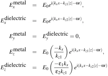
metal-dielectric interface are sustained. A cross section of the geometry is shown as an inset in Figure 1.1;
the metal is contained in the half spacez>0 with the metallodielectric interface located atz=0. Wave
prop-agation is along thexdirection. Assuming a perpendicularly polarized electric field incident on the structure,
the surface plasmon electric field takes the form
tific literature, few studies provide a coherent numerical comparison of dispersion, propagation, field skin depth, and energy density using empirically determined optical
con-stants. Here we present such data for an Ag/ SiO2 surface
plasmon excitation over the full wavelength range of Fig. 1. Properly considered, surface plasmons are the quanta of collective plasma oscillations localized at the interface be-tween a metal and a dielectric. Provided the thickness of the metal film exceeds the plasmon skin depth, oscillations at each metal-dielectric interface are decoupled, and indepen-dent surface plasmon modes at each metal-dielectric inter-face are sustained. A cross section of the geometry is shown as an inset in Fig. 2; the metal is contained in the half space
z⬎0 with the metallodielectric interface located at z= 0.
Wave propagation is along thexdirection.
Assuming a perpendicularly polarized electric field inci-dent on the structure, the surface plasmon electric field takes the form
E共x,z,t兲 ⬃E0ei共kxx−kz兩z兩−t兲 共3兲
with components given by
Emetal=E ei共kx−k 兩z兩−t兲, Edielectric=E ei共kx−k 兩z兩−t兲,
Ey metal
=Ey dielectric
= 0,
Ez metal
=E0
冉
−kx
kz1
冊
ei共kxx−kz1兩z兩−t兲,
Ezdielectric=E0
冉
−1kx
2kz1
冊
ei共kxx−kz2兩z兩−t兲.
Demanding continuity of the tangential E and normal D
fields at the interface yields the typical surface plasmon
dis-persion relations defined by22
kx=
c
冑
12
1+2
and kz21,2=1,2
冉
c
冊
2
−kx2. 共4兲
Provided 1
⬙
⬍兩1⬘
兩—a condition satisfied in Ag for ⬎328 nm in the Johnson and Christy data set and
⬎331 nm in the Palik set—the in-plane wave vector can be
written askx=kx⬘+ikx⬙, with
kx⬘=
c
冑
1
⬘
21
⬘
+2and kx⬙=
c
冉
1
⬘
21
⬘
+2冊
3/2冉
1⬙
21
冊
.
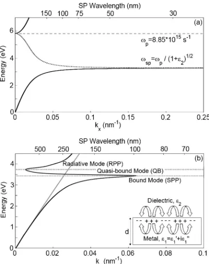
[image:27.612.219.434.205.476.2]共5兲 Figure 2共a兲 illustrates the dispersion characteristics for this mode, plotted using the dielectric function of a free electron
gas with p= 8.85⫻1015s−1.28 For energies below 3.3 eV,
the typical bound surface plasmon-polariton 共SPP兲mode is
observed, asymptoting at short wave vectors to the light line and at large wave vectors to the surface plasmon resonant
frequencySP共defined by the wavelength where1
⬘
= −2兲.Above 5.8 eV, the onset of the radiative plasmon-polariton
共RPP兲mode can be seen. For energies between the SPP and
RPP modes, the plasmon wave vector is purely imaginary 共represented as a dotted line in the figure兲, indicating that modes in this regime are forbidden. Historically, this region
betweenSPandp is referred to as the plasmon bandgap.
In contrast to the free electron behavior, dispersion arising from use of Johnson and Christy optical constants is plotted in Fig. 2共b兲. Though not shown, dispersion is nearly identical using the optical constants of Palik. For reference, the dis-persion curve for the SiO2 light line 共kx=2
1/2/ c兲 is also
included. Below 3.5 eV the SPP mode is observed, ap-proaching the light line at short wave vectors but terminating at a finite wave vector on resonance 共kx= 0.065 nm−1 at
SP兲.29As seen, the fairly large SPP wave vectors共and hence
small SPP wavelengths兲 achieved near resonance compete
with the largely reduced group velocity in this frequency range. Above 3.8 eV the RPP is observed, corresponding to
wavelengths satisfying the relation 1
⬙
⬎兩1⬘
兩 共i.e., ⬍328 nm兲. For energies between the SPP and RPP modes,kx
is determined by Eq.共4兲and what we term quasibound共QB兲
modes appear to exist. Unlike the imaginary modes of the FEG dispersion, the modes plotted here have mathematically
real components and hence are nota prioriforbidden.
Quasibound modes may provide an opportunity to study negative phase velocities in naturally occurring materials. Nevertheless, the seemingly infinite group velocity marking the transition regimes between SPP/QB modes and QB/RPP FIG. 2.共a兲Surface plasmon dispersion relation for the Ag/ SiO2
geometry computed using a free electron gas dispersion model. Note the existence of allowed modes共solid兲for frequencies below
SPand abovep, in contrast to the forbidden共i.e., purely imagi-nary兲modes between these frequencies共dotted兲.共b兲: Bound共SPP兲, radiative共RPP兲, and quasibound共QB兲surface plasmon dispersion relation for the Ag/ SiO2geometry computed using the optical con-stants of Johnson and Christy. Unlike the free electron dispersion of panel共a兲, modes are allowed throughout the entire frequency range shown. The SiO2light line共gray兲is also included for reference.
PLANAR METAL PLASMON WAVEGUIDES:… PHYSICAL REVIEW B72, 075405共2005兲
Figure 1.1:(a)Surface plasmon dispersion relation for the Ag/SiO2geometry computed
using a free electron gas dispersion model. Note the existence of allowed modes (solid) for frequences belowωSP and aboveωp, in contrast to the forbidden (i.e., purely imag-inary) modes between these frequencies (dotted). (b)Bound (SPP), radiative (RPP), and quasibound (QB) surface plasmon dispersion relation for the AgSiO2geometry
us-ing the optical constants of Johnson and Christy. Unlike the free electron dispersion of panel (a), modes are allowed throughout the entire frequency range shown. The SiO2
light line (gray) is also included for reference.
E(x,z,t)∼E0ei(kxx−kz|z|−ωt),
with components given by
Exmetal = E0ei(kxx−kz1|z|−ωt),
Exdielectric = E0ei(kxx−kz2|z|−ωt),
Eymetal = Eydielectric=0,
Ezmetal = E0
−kx
kz1
ei(kxx−kz1|z|−ωt), Ezdielectric = E0
−
ε1kx
ε2kz1
ei(kxx−kz2|z|−ωt).
The metal region is represented byε1=ε01+iε001 and correspondingkz1, while the dielectric hasε2and
kz2. Demanding continuity of the tangentialEand normalDfields at the interface yields the typical surface
plasmon dispersion relations defined by [114]
kx=
ω
c
r
ε1ε2 ε1+ε2
and k2z1,2=ε1,2
ω
c
2
−k2x. (1.21)
Providedε001<|ε01|— a condition satisfied in Ag forλ≥328 nm using the optical constants of Johnson
and Christy — the in-plane wave vector can be written askx=k0x+ik00x, with
k0x=ω
c
s
ε01ε2 ε01+ε2
and k00x=ω
c
ε0
1ε2 ε01+ε2
3/2
ε001
2ε1
. (1.22)
Figure 1.1(a) illustrates the dispersion characteristics for this mode, plotted using the dielectric function
of a free electron gas (FEG) withωp=8.85×10¹⁵s−1. For energies below 3.3 eV, the typical bound surface plasmon-polariton (SPP) mode is observed, asymptoting at short wave vectors to the light line and at large
wave vectors to the surface plasmon resonant frequencyωSP (defined by the wavelength whereε01=−ε2).
[image:28.612.230.415.199.330.2]the SPP and RPP modes, the plasmon wave vector is purely imaginary (represented as a dotted line in the
figure), indicating that modes in this regime are forbidden. Historically, this region betweenωSP andωpis referred to as the plasmon bandgap.
In contrast to the free electron behavior, dispersion arising from use of Johnson and Christy optical
con-stants is plotted in Figure 1.1(b). For reference, the dispersion curve for the SiO2light line (kx=ε12/2ω/c) is
also included. Below 3.5 eV the SPP mode is observed, approaching the light line at short wave vectors but
terminating at afinitewave vector on resonance (kx=0.065 nm−1atωSP). As seen, the fairly large SPP wave vectors (and hence small SPP wavelengths) achieved near resonance compete with the largely reduced group
velocity in this frequency range. Above 3.8 eV the RPP is observed, corresponding to wavelengths satisfying
the relationε001>|ε10|( i.e.,λ<328 nm). For energies between the SPP and RPP modes,kxis determined by Equation 1.21 and what we term ‘quasibound’ (QB) modes appear to exist. Unlike the imaginary modes of
the FEG dispersion, the modes plotted here have mathematically real components and hence are nota priori
forbidden.
Quasibound modes provide an opportunity to study negative phase velocities in naturally occurring
ma-terials [72]. Nevertheless, the seemingly infinite group velocity marking the transition regimes between
SPP/QB modes and QB/RPP modes is — at first sight — a disconcerting feature. In normal dispersive
me-dia, the group velocity is defined by the relationvg=dω/dk. However, in regions of anomalous dispersion this linearization does not apply, and the propagation velocity of the wave packet must be modified to account
for amplitude damping and wave profile deformation [134].
Figure 1.2 illustrates the propagation distance for an Ag/SiO2interface plasmon as a function of
wave-length for both the Johnson and Christy and Palik dielectric data sets. The surface plasmon intensity decreases
as exp(2ℜ[ikxx])so that the propagation length is given byL=|2ℜ[ikx]|−1. As seen, at the important tele-communications wavelength of 1550 nm, propagation distance approaches∼400µm using the Johnson and Christy dielectric function data set and∼70µm using Palik; at shorter wavelengths, both curves converge toward nanometer-scale propagation at the surface plasmon resonance. Thus, although large surface plasmon
wave vectors (and therefore short plasmon wavelengths) can be achieved near resonance, these attributes are
dispersive media, the group velocity is defined by the
rela-tion vg=d/dk. However, in regions of anomalous
disper-sion this linearization does not apply, and the propagation velocity of the wave packet must be modified to account for
amplitude damping and wave profile deformation.30 A
de-tailed discussion of QB mode properties 共including group
velocity and dispersion兲is deferred to another paper.
How-ever, these modes may exhibit significant physical effects on the time scale of short-lifetime plasmon processes, including plasmon decoherence by electron-hole pair generation and electron-phonon coupling.
Figure 3 illustrates the propagation distance for an
Ag/ SiO2 interface plasmon as a function of wavelength for
both the Johnson and Christy and Palik dielectric data sets.
The surface plasmon intensity decreases as exp共2 Re关ikxx兴兲
so that the propagation length is given byL=兩2 Re关ikx兴兩−1. As
seen, at the important telecommunications wavelength of
1550 nm, propagation distance approaches ⬃400m using
the Johnson and Christy dielectric function data set and
⬃70m using Palik; at shorter wavelengths, both curves
converge toward nanometer-scale propagation at the surface plasmon resonance. Thus, although large surface plasmon
wave vectors共and therefore short plasmon wavelengths兲can
be achieved near resonance, these attributes are often at the expense of propagation length.
Still, Fig. 3 does reveal the presence of a local maximum in propagation existing close to the plasmon resonant fre-quency. Indicating the transition between the QB and RPP modes, the neighborhood about this maximum corresponds to the region of anomalous dispersion in the silver dielectric constant. Accordingly, the relative magnitude of this maxi-mum can be controlled by altering the refractive index of the surrounding dielectric.
To illustrate the effects of varying the dielectric optical
Ag/Air, Ag/ SiO2, and Ag/ Si 共Ref. 31兲 interface plasmons
over the spectral range of 200– 500 nm. By using materials of varying refractive indices, the surface plasmon resonant frequency can be tuned through a broad spectral range. As a result, the energetic location of the maxima and minima in the propagation distance plot can be controlled. Alterna-tively, at a given frequency, the surface plasmon wavelength 共and hence damping兲can be tuned by the dielectric constant. Such results suggest that by altering the optical properties of the embedding dielectric共i.e., with an electro-optic material兲, propagation might be dynamically switched under optical pumping. However, significant shifts for thick films require
refractive index differentials of order ⌬n= 0.132: at a free
space wavelength of = 1550 nm, such index contrast can
lead to a 6m change in propagation length.
The inset also reveals that for a given free-space wave-length, the longest propagation lengths are achieved for in-sulating materials with the smallest dielectric constant.
How-ever, combining data as in Figs. 2共b兲 and 3 for various
dielectrics共data not shown兲, we find that the optimal
combi-nation of small plasmon wavelength and low damping is observed for a dielectric with the largest refractive index.
Figure 4 plots the surface plasmon electric field skin
depth 共1 /edecay length兲in both Ag and SiO2as a function
of wavelength. Note that in this graph, decay into the metal
is plotted below z= 0. For clarity, the figure only includes
skin depth computed using the JC data set. As expected, the SPP skin depth into the dielectric increases with increasing
wavelength, reaching values of 1.3m共1.1m兲in SiO2 at
vac= 1550 nm for the JC 共Palik兲 data sets, respectively. In
contrast, the SPP skin depth into the metal remains roughly
constant at ⬃20 nm 共25 nm兲 for wavelengths beyond the
plasmon resonance. At resonance, field penetration in the metal reaches a minimum in both the metal and dielectric 共with z⬃15 nm for both Ag and SiO2兲. For even shorter
FIG. 3. Surface plasmon propagation length for the Ag/ SiO2 geometry calculated using the optical constants of Johnson and Christy共solid兲and Palik 共dotted兲. A vanishing propagation length occurs at the surface plasmon resonance, located at = 355 nm
共358 nm兲 for Palik 共JC兲. The local maximum at⬃320 nm coin-cides with the transition between QB and RPP modes. Inset: Com-parison of SP propagation for Ag/Air, Ag/ SiO2, and Ag/ Si geom-etries plotted about the SP resonance.
FIG. 4. Surface plasmon electric field penetration depth into Ag and SiO2, computed using the dielectric data of Johnson and Christy. The local penetration maximum at shorter wavelengths cor-responds to the transition between the quasibound and radiative surface plasmon modes.
DIONNEet al. PHYSICAL REVIEW B72, 075405共2005兲
Figure 1.2: Surface plasmon propagation length for the Ag/SiO2geometry calculated
using the optical constants of Johnson and Christy (solid) and Palik (dotted). A van-ishing propagation length occurs at the surface plasmon resonance, aroundλ=355 nm. The local maximum atλ∼320nm coincides with the transition between QB and RPP modes. Inset: Comparison of SP propagation for Ag/Air, Ag/SiO2, and Ag/Si
geometries plotted about the SP resonance.
Still, Figure 1.2 does reveal the presence of a local maximum in propagation existing close to the plasmon
resonant frequency. Indicating the transition between the QB and RPP modes, the neighborhood about this
maximum corresponds to the region of anomalous dispersion in the silver dielectric constant. Accordingly,
the relative magnitude of this maximum can be controlled by altering the refractive index of the surrounding
dielectric.
To illustrate the effects of varying the dielectric optical constant, the inset of Figure 1.2 plots propagation
lengths for Ag/Air, Ag/SiO2, and Ag/Si interface plasmons over the spectral range of 200 to 800 nm. By using
materials of varying refractive indices, the surface plasmon resonant frequency can be tuned through a broad
spectral range. As a result, the energetic location of the maxima and minima in the propagation distance plot
can be controlled. Alternatively, at a given frequency, the surface plasmon wavelength (and hence damping)
can be tuned by the dielectric constant. Such results suggest that by altering the optical properties of the
embedding dielectric, propagation might be dynamically switched under electrical bias or optical pumping.
Figure 1.3 plots the surface plasmon electric field skin depth (1/edecay length) in both Ag and SiO2as a
function of wavelength. Note that in this graph, decay into the metal is plotted belowz=0. For clarity, the
figure only includes skin depth computed using the Johnson and Christy data set. As expected, the SPP skin
dispersive media, the group velocity is defined by the
rela-tion vg=d/dk. However, in regions of anomalous
disper-sion this linearization does not apply, and the propagation velocity of the wave packet must be modified to account for
amplitude damping and wave profile deformation.30 A
de-tailed discussion of QB mode properties 共including group
velocity and dispersion兲is deferred to another paper.
How-ever, these modes may exhibit significant physical effects on the time scale of short-lifetime plasmon processes, including plasmon decoherence by electron-hole pair generation and electron-phonon coupling.
Figure 3 illustrates the propagation distance for an
Ag/ SiO2 interface plasmon as a function of wavelength for
both the Johnson and Christy and Palik dielectric data sets.
The surface plasmon intensity decreases as exp共2 Re关ikxx兴兲
so that the propagation length is given byL=兩2 Re关ikx兴兩−1. As
seen, at the important telecommunications wavelength of
1550 nm, propagation distance approaches⬃400m using
the Johnson and Christy dielectric function data set and
⬃70m using Palik; at shorter wavelengths, both curves
converge toward nanometer-scale propagation at the surface plasmon resonance. Thus, although large surface plasmon
wave vectors共and therefore short plasmon wavelengths兲can
be achieved near resonance, these attributes are often at the expense of propagation length.
Still, Fig. 3 does reveal the presence of a local maximum in propagation existing close to the plasmon resonant fre-quency. Indicating the transition between the QB and RPP modes, the neighborhood about this maximum corresponds to the region of anomalous dispersion in the silver dielectric constant. Accordingly, the relative magnitude of this maxi-mum can be controlled by altering the refractive index of the surrounding dielectric.
To illustrate the effects of varying the dielectric optical
Ag/Air, Ag/ SiO2, and Ag/ Si 共Ref. 31兲 interface plasmons
over the spectral range of 200– 500 nm. By using materials of varying refractive indices, the surface plasmon resonant frequency can be tuned through a broad spectral range. As a result, the energetic location of the maxima and minima in the propagation distance plot can be controlled. Alterna-tively, at a given frequency, the surface plasmon wavelength 共and hence damping兲can be tuned by the dielectric constant. Such results suggest that by altering the optical properties of the embedding dielectric共i.e., with an electro-optic material兲, propagation might be dynamically switched under optical pumping. However, significant shifts for thick films require
refractive index differentials of order ⌬n= 0.132: at a free
space wavelength of = 1550 nm, such index contrast can
lead to a 6m change in propagation length.
The inset also reveals that for a given free-space wave-length, the longest propagation lengths are achieved for in-sulating materials with the smallest dielectric constant.
How-ever, combining data as in Figs. 2共b兲 and 3 for various
dielectrics共data not shown兲, we find that the optimal
combi-nation of small plasmon wavelength and low damping is observed for a dielectric with the largest refractive index.
Figure 4 plots the surface plasmon electric field skin
depth共1 /edecay length兲in both Ag and SiO2as a function
of wavelength. Note that in this graph, decay into the metal
is plotted below z= 0. For clarity, the figure only includes
skin depth computed using the JC data set. As expected, the SPP skin depth into the dielectric increases with increasing
wavelength, reaching values of 1.3m共1.1m兲 in SiO2at
vac= 1550 nm for the JC 共Palik兲 data sets, respectively. In
contrast, the SPP skin depth into the metal remains roughly
constant at ⬃20 nm 共25 nm兲 for wavelengths beyond the
plasmon resonance. At resonance, field penetration in the metal reaches a minimum in both the metal and dielectric 共with z⬃15 nm for both Ag and SiO2兲. For even shorter
FIG. 3. Surface plasmon propagation length for the Ag/ SiO2 geometry calculated using the optical constants of Johnson and Christy共solid兲 and Palik共dotted兲. A vanishing propagation length occurs at the surface plasmon resonance, located at = 355 nm
共358 nm兲 for Palik共JC兲. The local maximum at⬃320 nm coin-cides with the transition between QB and RPP modes. Inset: Com-parison of SP propagation for Ag/Air, Ag/ SiO2, and Ag/ Si geom-etries plotted about the SP resonance.
FIG. 4. Surface plasmon electric field penetration depth into Ag and SiO2, computed using the dielectric data of Johnson and Christy. The local penetration maximum at shorter wavelengths cor-responds to the transition between the quasibound and radiative surface plasmon modes.
DIONNEet al. PHYSICAL REVIEW B72, 075405共2005兲
Figure 1.3: Surface plasmon electric field penetration depth in Ag and SiO2, computed
using the dielectric data of Johnson and Christy. The local penetration maximum at shorter wavelengths corresponds to the transition between the quasibound and radiative surface plasmon modes.
depth into the dielectric increases with increasing wavelength, reaching values of 1.3µm (1.1µm) in SiO2at
λvac=1550 nm for the Johnson–Christy (Palik) data sets, respectively. In contrast, the SPP skin depth into
the metal remains roughly constant at∼25 nm for wavelengths beyond the plasmon resonance. At resonance, field penetration in the metal reaches a minimum in both the metal and dielectric (withz∼15 nm in both Ag and SiO2). For even shorter wavelengths, field penetration reaches a maximum in the metal and a local
maximum in SiO2(zAg∼60 nm,zSiO2∼40 nm) forλ∼330 nm — a wavelength regime corresponding to
anomalous Ag dispersion and marking the onset of the radiative plasmon polariton.
This observation raises an interesting distinction between the system resonances corresponding to the
extrema in the plot of propagation length versus wavelength (i.e., the local maximum and the global
mini-mum in Fig. 1.2). At one system resonance, corresponding to anomalous dispersion, propagation is slightly
enhanced despite high field confinement within the metal. However, at the surface plasmon resonance,
propa-gation approaches single nanometer scales despite minimal energy density within the metal. The latter result
is explained by the vanishing SPP excitation group velocity near the plasmon resonance. Still, the
contradic-tion to the common localizacontradic-tion versus loss heuristic is evident: field localizacontradic-tion within the metal does not
necessarily result in increased loss.
1.5
Scope of this Thesis
The work presented in this thesis falls into two broad categories. First is development of numerical methods
for analysis of plasmonic nanostructures. Second is the design and characterization of plasmonic devices,
with the broad and general goal of creating a significant impact in the fields of optoelectronics and
photo-voltaics. The two pursuits are, of course, intimately related. As the experimental state of the art has progressed
from basic physical studies to the prototyping of various functional plasmonic devices, so too has the demand
for numerical solutions evolved to include tools for quantitative prediction of practical figures of merit. The
thesis is divided into three main parts:
1.5.1
Part I: Numerical Analysis Methods
Here, an overview is presented of the various numerical methods which will be employed systematically
throughout the rest of the thesis. The methods discussed here are post-processing or algorithmic methods
which can be applied to time-domain numerical data; in principle this process is independent of which
com-mercial or custom software platform is used as a calculation engine. On a broad scale, these techniques
parallel established methods in the RF computational electrodynamics literature, which are not
necessar-ily discussed widely in the plasmonics community. This section will also highlight a variety of extensions
specific to a nanophotonic design “toolbox,” and in several cases reference experimental studies which
cor-roborate the numerical analysis.
Chapter 2 develops techniques to analyze resonant nanostructures, such as small metal particles. The
principal technique employed is impulse excitation ringdown spectroscopy, which allows the critical
advan-tage of generating broadband spectra from a single time-domain simulation. Once the resonance spectrum
is determined, time-domain techniques can also be used to find cavity parameters such as the local field
enhancement factor f, effective mode volumeV, and quality factorQ.
In Chapter 3, simulations of plasmonic waveguiding structures are studied. Fourier-space analysis is
used to reveal the dispersion properties of waveguides, and to perform mode filtering. Full-field simulation
is most valuable as a tool for characterizing non-analytic geometries, such as the incoupling to waveguides
isolate scattered fields from a subwavelength object. Numerical calculation of the local energy dissipation
via divergence of the Poynting vector is introduced as a metric for differentiating thermal loss from “good”
absorption, e.g., in a solar cell.
1.5.2
Part II: Resonant Plasmonic Nanostructures
The theme of Part II is resonant plasmonic nanostructures, especially small metal nanoparticles. The first
two chapters explore the plasmonic resonances of nanoparticles which act as very strongly coupled dipole
scatterers, in order to achieve extreme enhancement of the local electromagnetic field. The strongest local
field confinement comes from very small particles which are very close together, and to this end (Chapter
4) describes an unusual fabrication technique in which high-energy ion beam irradiation is used to form
linear chains of 10 nm Ag particles, only a few nm apart, in a glass matrix. We indeed observe very strong
anisotropy in the optical properties of the glass. Finite element finite difference time-domain (FDTD) methods
employing impulse-excitation ringdown spectroscopy are used to correlate the observed nanostructure and
spectral data in Chapter 5, building confidence in the use of FDTD to describe the local electromagnetic
environment of the tiny particle arrays.
In Chapter 6 the focus changes from basic science to an intriguing application. Theory predicts that the
radiative rate of a dipolar emitter, such as that of nanocrystalline Si, can be modified by near-field coupling
to a passive dipole, such as an Ag nanoparticle. Finite element methods are used as a design tool to help
generate an “nanoantenna” array of metal particles with variable resonant frequency. The observed optical
extinction spectra of the fabricated arrays provide additional confirmation of the accuracy of the
impulse-ringdown method. Furthermore, the simulated field enhancement is found to correctly predict the actual
photoluminescence enhancement, supporting the predictive power of our numerical method. In Chapter 7,
impulse-ringdown spectroscopy is successfully applied to analysis of an entirely different form of
1.5.3
Part III: Guided-Wave Plasmonics
Part III deals with analysis of guided wave plasmonics. Chapter 8 introduces metal/insulator/metal (MIM) or
“plasmon slot” waveguides via a semi-analytic numerical solution. These waveguides are rapidly becoming
a staple of nascent plasmonic device applications due to favorable trade-off between confinement of fields to
the dielectric core, and relatively low loss. This chapter also serves to provide context for the applicability of
full-field time domain simulation in MIM applications. Since the characterization of steady-state waveguide
modes proves analytically tractable, the great value for FDTD analysis is in low-symmetry structures such as
Part I
Chapter 2
Impulse Excitation Analysis of
Resonators
2.1
Introduction
This chapter reviews numerical methods used to generate the wide-band spectral response from a single time
domain simulation of a plasmonic resonator1. Here, we will focus initially on the simple example of a small,
spherical metallic shell.
A plasmonic resonator, such as our exemplary metal shell, acts as a damped, harmonic oscillator. The
free electrons in the metal feel a driving force in the presence of an applied electromagnetic field, and a
restorative force that depends on the resulting induced non-equilibrium polarization. The resonant frequency
is an intrinsic property of the particle and depends on the shape and the optical properties of the particle itself,
and of its dielectric environment.
In order to find the resonant frequency, we need to generate an appropriate impulse function. Consider the
case of an analogous harmonic oscillator, a damped mechanical spring, for which the appropriate initializing
impulse would be a state where the spring is stretched and suddenly released. The resonance frequency
of the spring can be observed by monitoring the length of the spring as a function of time as it oscillates,
or “rings down,” following the impulse excitation. In the case of our metallic particle, the corresponding
impulse excitation is the spontaneous application of a non-equilibrium charge distribution. We will present
the method in which we can generate this impulse initialization in finite-element time domain electromagnetic
calculations and analyze the resulting ringdown response.
2.2
Impulse Excitation, Resonant Ringdown Method
Our sample resonant structure is a metallodielectric “core-shell” particle, that is, a metal sphere, composed
of a dielectric core surrounded by a metallic shell. The plasmon frequency of these particles can be tuned
throughout the visible and near-infrared part of the spectrum by varying core diameter and shell thickness [1,
91, 96]. Additional tuneability can be obtained by shape anisotropy, which induces a splitting of the plasmon
resonance in red-shifted longitudinal and blue-shifted transverse plasmon bands [14, 103, 104, 139].
The inner radius isRcore =228 nm; the shell itself is a layer of Au with thicknesstAu=38 nm. The
core material and the surrounding medium are both considered as a dielectric with indexn=1.45, while the
optical response of Au is determined with a Drude model:
ε(ω) =εd−
ω2p
ω2+iωγ (2.1)
withεd=9.54,ωp=1.3×10¹⁶ rad/s, andγ=1.25×10¹⁴ rad/s. This structure is input into a commer-cial finite element time-domain software package [48] with a graded mesh to minimize any error due to
discretization of the curved surface.
We next seek to initialize resonant “ringdown” of our particle by applying an impulsive excitation. This
technique is motivated by a common method in the radiofrequency (RF) time domain computation
litera-ture, in which the broadband frequency response of an antenna can be found by driving it with a Gaussian
modulated pulse. The finite length of the pulse in the time domain is Fourier equivalent to a wide band
excitation. Using an initialization procedure which is conceptually similar but employs an effectively
instan-taneous impulse, the strategy is to instaninstan-taneously apply a non-equilibrium polarization charge distribution to
the particle that is similar to the charge distribution of the particle’s natural mode(s) of resonance. In practice
to build up such an impulse, the simulation volume is illuminated with a low-frequency source, switched on
gradually and allowed to come to steady-state. The source may be either a plane wave or a point dipole, and
struc-Figure 1
Figure 2.1: Impulse excitation ringdown spectroscopy of a metallic shell. In panel (a), the x-component of the electric field, Ex, of a plane wave propagating in the y-direction, at a frequen