This is a repository copy of
Performance improvements of a split-off band infra-red
detector using a graded barrier
.
White Rose Research Online URL for this paper:
http://eprints.whiterose.ac.uk/78936/
Version: Published Version
Article:
Pitigala, PKDDP, Lao, YF, Perera, AGU et al. (3 more authors) (2014) Performance
improvements of a split-off band infra-red detector using a graded barrier. Journal of
Applied Physics, 115 (6). 063105. ISSN 0021-8979
https://doi.org/10.1063/1.4865501
[email protected] https://eprints.whiterose.ac.uk/ Reuse
Unless indicated otherwise, fulltext items are protected by copyright with all rights reserved. The copyright exception in section 29 of the Copyright, Designs and Patents Act 1988 allows the making of a single copy solely for the purpose of non-commercial research or private study within the limits of fair dealing. The publisher or other rights-holder may allow further reproduction and re-use of this version - refer to the White Rose Research Online record for this item. Where records identify the publisher as the copyright holder, users can verify any specific terms of use on the publisher’s website.
Takedown
If you consider content in White Rose Research Online to be in breach of UK law, please notify us by
Performance improvements of a split-off band infra-red detector
using a graded barrier
P. K. D. D. P. Pitigala,1Y. F. Lao,1A. G. U. Perera,1,a)L. H. Li,2E. H. Linfield,2and H. C. Liu3
1Department of Physics and Astronomy, Georgia State University, Atlanta, Georgia 30303, USA 2School of Electronic and Electrical Engineering, University of Leeds, Leeds LS2 9JT, United Kingdom 3Department of Physics, Shanghai Jiao Tong University, Shanghai, China
(Received 14 November 2013; accepted 31 January 2014; published online 12 February 2014)
Uncooled split-off band infrared detectors have been demonstrated with an operational device response in the 3–5lm range. We have shown that it is possible to enhance this device response
through reducing the recapture rate by replacing one of the commonly used flat barriers in the device with a graded barrier, which was grown using a “digital alloying” approach. Responsivity of approximately 80lA/W (D*¼1.4108Jones) were observed at 78 K under a 1 V applied
bias, with a peak response at 2.8lm. This is an improvement by a factor of25 times compared
to an equivalent device with a flat barrier. This enhancement is due to improved carrier transport resulting from the superlattice structure, and a low recapture rate enabled by a reduced distance to the image force potential peak in the graded barrier. The device performance can be further improved by growing a structure with repeats of the single emitter layer reported here.
VC 2014 AIP Publishing LLC. [http://dx.doi.org/10.1063/1.4865501]
I. INTRODUCTION
The development of infrared (IR) detectors operating at or around room temperature would be of great benefit for many practical applications, reducing the weight and power requirements of cooling systems. Different types of semicon-ductor structure, including those based on bulk HgCdTe,1,2 quantum well,3–6quantum dot,7,8and type-II strained super-lattices,9 have been studied and tested in an attempt to achieve this aim. In addition, theoretical studies have been undertaken to understand and try to solve the problems asso-ciated with achieving uncooled IR detection.10,11Recently, a split-off band detector with a 4lm threshold wavelength,
was successfully demonstrated operating up to room temper-ature.12However, the performance was low owing to exces-sive carrier recapture in the emitters.
Split-off band detectors consist of highly p-doped emit-ters separated by undoped barriers. The photo-absorption in the emitter excites carriers from the light/heavy hole bands into the split-off band. These excited carriers then escape into the barrier region, typically after scattering back into the light/heavy hole band at the emitter-barrier interface, and are collected at the contact regions using an applied electric field. The IR response arising from split off band transitions in a p-doped GaAs/Al0.12Ga0.88As heterostructure was
ini-tially reported by Pereraet al.at 77 K.13 Thereafter, higher operating temperature split-off band IR detectors were dem-onstrated by Jayaweeraet al.12 using high aluminum mole
fractions (x), where x¼0.28, 0.38, and 0.57, in the
AlxGa(1x)As barriers; this led to devices operating uncooled
with x¼0.57. Subsequently, Matsik et al.14 theoretically predicted a two orders in magnitude improvement in the de-vice response, and a three orders in magnitude increase in
the detectivity (D*), by introducing graded and resonant tun-neling barriers into the split-off band device architecture. Furthermore, a theoretical study on dark current mechanisms in split-off band devices conducted by Laoet al.15suggested that use of small mesas and high doping can result in sup-pression of the 2-D carrier transport, which leads to high dark currents.
As Matsik et al.14 proposed, one possible approach to improve the performance of detectors is to use a graded bar-rier for the injection. The extra kinetic energy of carbar-riers entering over the high-sided barrier should reduce the excess trapping leading to photoconductive gain through a mecha-nism similar to that observed in QWIPs.16 Furthermore, if the graded barrier on the injection side is higher than that on the escape side, artificially heated carriers will enter the emitter. Providing that there is a sufficiently large potential difference between the two edges of the barrier, excited car-riers will then be able to escape after scattering; hence, the trapping rate will be reduced. Additionally, the gradient in the barrier will allow the thermal escape carriers from the contact and the carriers in the emitter to be in equilibrium, resulting in reduced space charge buildup.14 In such struc-tures, the graded barriers can be grown using two different approaches that can be categorized as (1) “digital alloy,”17 where the structure consists of short-period superlattices of GaAs/AlAs binary layers with periods of a few monolayers thickness, and (2) “non-digital alloy,” where the structure does not have any short-period superlattices.
Our study here reports experimental results for a split-off band detector with a graded barrier. The effects on device performance of using different techniques to grow the graded barrier will also be discussed. These results provide valuable information on the strategies that can be adopted to increase further the performance of uncooled split off band devices, and we will show, through comparison of results with simu-lation,14that further improvements are possible.
a)Author to whom correspondence should be addressed. Electronic mail:
II. EXPERIMENTAL PROCEDURE
A. Device structures
Three devices, identified as 0906, 1001, and 1007 (pa-rameters given in TableI), with a single emitter sandwiched between two barriers were studied to understand: (1) the effects of a graded barrier, and (2) the effects of the use of “digital alloying” during barrier growth on device perform-ance. In all structures one of the two barriers (h3) was kept
flat as shown in Fig.1, at a barrier height 240 meV. The sec-ond barrier in 0906 and 1007 has a gradient, where the low-est end (h1) is adjacent to the bottom contact and the highest
end (h2) is adjacent to the emitter side. The valance band
dia-gram of the graded barrier devices is shown in Fig.1(a)and the barrier heights at the two ends (h1 and h2) are listed in
TableI. In the third device, 1001, the second barrier is kept flat, as shown in the band diagram in Fig.1(b), with a barrier height 390 meV.
Both barriers in samples 1001 and 1007 were grown using “non-digital alloying” and these are used to compare the performance of the graded barrier structure with flat bar-rier structures. In 0906 the graded barbar-rier is grown with a “digital alloying” approach and this is compared with 1007 to correlate device performance with the use of “digital-alloying” and “non-digital “digital-alloying” approaches.
B. Digital alloying and non-digital alloying approaches of growth
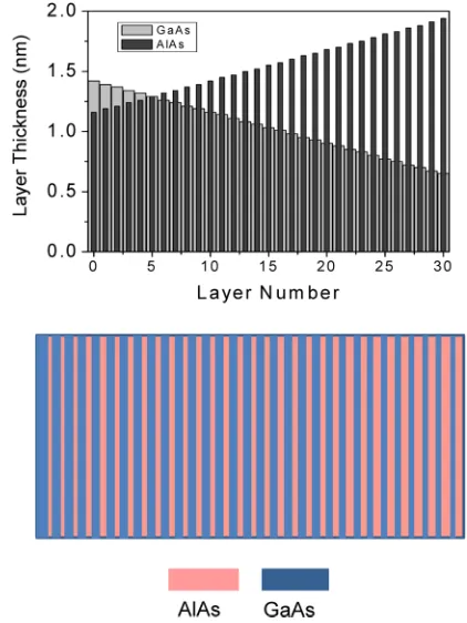
The “digital alloying” formula used in the graded barrier growth of 0906 is as follows: 31 periods of GaAs and AlAs
with thicknesses (0.45þ0.01N)L/31 and (0.550.01N)
L/31, respectively, where N is the number of the period and L is the total thickness of the graded barrier. This gives a
total single period thickness of 2.6 nm, and a minimum
AlAs layer thickness of0.6 nm, for L¼80 nm. The number of periods chosen for the superlattice is a compromise. If N is reduced (increased), the individual layers become wider (narrower) and quantum states are likely to appear within the barrier region, resulting in the structure no longer behaving like a graded alloy. Furthermore, if the number of periods is increased, it will be difficult to grow reproducibly the thin-nest layers in the structure. Approximate GaAs and AlAs layer thicknesses, and a schematic diagram of the layer arrangement in the graded barrier region, are shown in Fig.2. The final five periods were grown by dividing the layers into four sub periods using the same total barrier and emitter thickness as determined from the above formula to prevent the thickness of the GaAs layers becoming thicker
FIG. 1. Schematic diagram of the band alignment in the structures: (a) the graded barrier structure, (b) the flat barrier structure. The device parameters are tabulated in TableI. All samples have contact regions doped to 11019cm3, an 80 nm wide graded barrier (h1-h2), an 80 nm wide emitter p-doped to
11019cm3, and a 400 nm wide flat barrier (h
[image:3.612.51.296.168.250.2]3) with height 240 meV.
TABLE I. Sample parameters and activation energies calculated from Arrhenius plot for the tested devices. The graded barrier heights at the two ends of the detector structures are 240 meV at the contact end (h1) and
390 meV at the emitter end (h2), as shown in the band diagram (Fig.1). All
samples have contact regions doped to 11019cm3, an 80 nm wide graded barrier, an 80 nm wide emitter p-doped to 11019cm3, and a 400 nm wide flat barrier with a height (h3) of 240 meV. Acronyms used for the alloying
method used in the graded barrier are: Dig.: Digital alloying approach; and Non-Dig.: non-digital alloying approach. The expected value of the activa-tion energy is39065 meV for the devices.
Sample
Alloying method
Barrier height (meV) Activation energy (meV) h1 h2 h3
[image:3.612.330.541.442.723.2]0906 Dig. 240 390 240 470610 1007 Non-Dig. 240 390 240 380610 1001 Non-Dig. 390 390 240 280610
FIG. 2. Graphical representation of the GaAs and AlAs layer thicknesses in the “averaging” approach, and a schematic of the layer arrangement. The histogram shows the variation of the GaAs and AlAs layer thicknesses at each layer number in the digital alloyed graded barrier.
[image:3.612.52.299.498.714.2]than the AlAs layers. In this structure, carriers only see an average aluminum fraction for several adjacent layers,17i.e., when layers are in the range of an atomic layer thickness, one layer of GaAs and two layers of AlAs would affect a car-rier like a bulk Al0.67Ga0.33As layer. Additionally, the rough
and partial AlAs/GaAs interfaces will break up any miniband formation, and hence improve the averaging behavior.
The flat barrier device (1001) and the graded barrier de-vice (1007) were grown using a non-digital alloying approach, where the changing aluminum fraction (the gradi-ent) is obtained by gradually changing the temperature, and hence deposition rate, of the aluminum cell.
C. Measurements and characterization
The current-voltage-temperature (IVT) measurements on the devices were carried out by mounting the devices on a closed cycle refrigerator, connected to a Lake Shore 330 temperature controller. A Keithley 2400 source meter was used to apply the bias voltage and measure the current flow in the device. IVT measurements are used to estimate the dark current and hence determine the barrier height using Arrhenius plots.
The spectral measurements of the devices were con-ducted by mounting the device in a liquid helium cooled dewar and scanning the device response using a Perkin Elmer system 2000 Fourier transform infrared (FTIR) spec-trophotometer. The device was biased using an external DC power supply, and temperature was controlled by a Lake Shore 330 temperature controller. The device spectral response is calibrated using a silicon bolometer mounted in the same dewar and operated under similar conditions.
The specific detectivity (D*) is a figure of merit used to calculate performance of photo-detectors. Higher D* implies better performance in the device. D* can be given as:
D¼
ffiffiffiffiffi
Af
p
NEP; (1)
where A is the photosensitive area of the device, f is the fre-quency bandwidth and NEP is the noise equivalent power. The NEP can be written as a ratio of the responsivity (R) to the noise spectral density (S(f)) of the device. Therefore, the specific detectivity (D*) of the device can be given as
D¼ <
ffiffiffi
A
p
ffiffiffiffiffiffiffiffiffi
SðfÞ
p : (2)
In this case S(f) is the shot noise in the device calculated by S(f)¼4qI, where q and I are the electron charge, and dark current of the device, respectively. D* is then the shot noise limited detectivity.
III. RESULTS AND ANALYSIS
A. Comparison of results for graded and flat barriers
The current-voltage (IV), responsivity and detectivity (D*) of the graded barrier structure (1007) and the flat barrier structure (1001), grown with a “Non-Digital Alloying”
approach, were compared at 78 K for devices with similar dimensions (including the emitter thickness of 80 nm). The asymmetry in the I-V characteristics (Fig. 3) is due to the asymmetric barriers in the structures. As the bias voltages increase, 1007 shows a higher dark current compared to 1001. Decrease in the effective barrier height under negative bias and a decrease of the effective barrier width as the gra-dient increases under positive bias assist the carrier tunneling through the graded barrier. As a result, the breakdown volt-age is reached at a lower bias voltvolt-age in 1007, compared to the 1001. Furthermore, the shoulder like feature in the I-V curves at around aþ10 V bias confirms the excess tunneling of carriers in the graded barrier device.
Table I shows that the activation energies calculated from Arrhenius plots are approximately 470 and 380 meV for 1001 and 1007, respectively. Structure 1007 has its acti-vation energy close to the expected barrier height of 390 meV, whilst in 1001 there is a higher activation energy than expected. The reason for this high activation energy in 1001 is not fully understood.
The responsivities for 1001 and 1007 at 78 K, atþ1 V and 1 V biases, are shown in Figs.4(a) and4(b), respec-tively. The peak values, at a wavelength of 2.8lm, for each
device are listed in TableII. Even though the activation ener-gies are different in structures 1001 and 1007, the response thresholds do not show a significant shift between the two devices, except for the0.1lm red shift in 1007 at positive
bias. At negative bias, threshold wavelengths are6.5lm in
both cases. Structure 1007 has a higher responsivity of
2105A/W and 4.2105A/W, under 1 V and 1 V
biases, compared to 1001, where the responsivities are 1.9106A/W and 6.2106A/W, respectively.
In summary, device 1007 has a high responsivity and D* compared to 1001 under both negative and positive bias, indicating that the integration of a graded barrier is enhanc-ing the device performance.
B. Comparison of digital alloying and non-digital alloying approaches
[image:4.612.344.530.574.720.2]The effect of using a digital alloying approach for the graded barrier (0906), compared with a non-digital alloying
approach (1007), was investigated, with all other aspects of the devices remaining identical. Fig.3shows the IV charac-teristics of 0906, where the dark current at higher biases increases rapidly compared to 1007. In addition, the IV curve of 0906 shows a shoulder like feature due to tunneling, which is observed at a lower bias voltage compared to the 1007, indicating dominant tunneling paths in 0906 compared to the 1007. Furthermore, the activation energy calculated for 0906 is 280 meV which is smaller than the expected value for the barrier height (390 meV) in the device. This low activation energy can be caused by tunneling paths in the barrier.
A TEM image of the graded barrier region for the wafer grown with a “digital alloying” approach is shown in Fig.5. The layer separation is not clearly visible in the topmost region of the barrier (periods 25 to 31), where a finer mesh digital grading was used in the last five of the 31 periods. Here, the thinner layers of the sub-periods are below the re-solution limits. In the first 25 periods, however, the TEM
image shows an uneven layer separation between the GaAs and AlAs layers in some areas of the structure. These uneven areas, with thicker GaAs and thinner AlAs layers, can pro-vide a tunneling path for carriers through the barrier.
The responsivity of 0906 underþ1 V and1 V biases is shown in Figs.4(a)and4(b). The response threshold of 0906 is red shifted compared to the response threshold of 1007 due to the reduced barrier height in the 0906, as indicated by the lower activation energy. The responsivity at a wave-length of 2.8lm is shown in Table II for each bias, with
0906 having the highest responsivities of all three structures, with values of 7.8105A/W and 4.9105A/W at1 V and 1 V biases, respectively. This is approximately a factor of two improvement compared to 1007. The shot noise lim-ited detectivity (D*) for 0906 at 78 K is given in the TableII,
and the D* values are evaluated as 3.4108 Jones and
8.2108Jones at1 V and 1 V biases, respectively.
C. Room temperature performance of the devices
[image:5.612.81.265.60.357.2]IV characteristics of 0906, 1007 and 1001 at room tem-perature (300 K) are shown in the Fig.6. A very large dark current was observed in 0906 compared to 1007 and 1001, both under positive and negative bias. Additionally, the asymmetry observed in the IV curves at 78 K is not promi-nent at 300 K. This indicates that the 80 nm thin barriers, which created the asymmetry in the devices, are depleted, and only the thick 400 nm barrier (h3) is effectively active in FIG. 4. The responsivity of the devices 0906, 1001, 1007 at 78 K: (a) under
positive bias, and (b) negative bias. At positive bias all three devices have shown a peak response around 2.7lm, whilst under negative bias all three
[image:5.612.341.534.63.258.2]devices have additional response peaks around 4.9lm. 0906 gave the high-est responsivity among the devices.
TABLE II. The shot noise density, calculated by S(f)¼4qI, the responsivity and the D* of devices at 78 K underþ1 V and1 V bias.
Shot noise (A2/Hz) Responsivity (A/W) Detectivity (D*) Jones
1 V 1 V 1 V 1 V 1 V 1 V
[image:5.612.50.562.686.765.2]1001 1.01030 2.21030 1.91006 6.21006 5.010þ07 1.110þ08 1007 2.41030 1.21029 2.01005 4.21005 3.310þ08 3.110þ08 0906 2.41030 3.51029 4.81005 7.81005 8.210þ08 3.410þ08 FIG. 5. TEM image of the graded barrier showing the layer separation in the “digital alloyed” graded barrier. A clear layer separation between GaAs and AlAs layers are visible in the structure except for the topmost region of the barrier, where a finer mesh digital grading was used.
these devices. This leads to the observed symmetry in dark current flow under positive and negative bias. The response of all three devices was very weak at 300 K because of the very high dark current.
IV. DISCUSSION
A. Response and carrier transport in the structures and the effects of the graded barrier
The observed device responses originate from split-off and heavy hole/light hole (hh/lh) transitions in p-doped GaAs.18The extended wavelength response beyond the bar-rier height (activation energy) is a result of hh/lh transi-tions.18 Therefore, the two peaks observed in the response
spectrum arise from split-off transitions (wavelength
<3.5lm) and hh/lh transitions which enable the long
wave-length response (>3.5lm). Long wavelength response
thresholds are shifted between devices because of differences in the effective barrier heights.
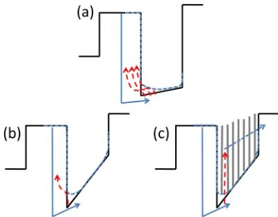
The higher photoresponsivity and longer wavelength response thresholds observed in the devices at negative bias, compared to positive bias, can be explained by ana-lyzing the possible carrier transport paths of the devices, as illustrated in Fig. 7. Fig. 7(a) shows, under negative bias, that carriers will be excited from both the bottom contact (BC) layer and the emitter. A portion of the excited carriers from the BC will transport over the emit-ter region without trapping. These carriers will combine with the stream of carriers excited from the emitter result-ing in a higher photocurrent at negative bias. Furthermore, the carriers excited from the emitter under negative bias only encounter the low barrier (h3) resulting in the long
wavelength response threshold. In contrast, under positive bias, carriers excited from the top contact (TC) will be trapped at the emitter, and only the carriers excited from the emitter will contribute to the photocurrent; hence, the photocurrent is lower. In addition, these carriers have to overcome the highest barrier edge (h2) resulting in a
shorter wavelength response threshold compared to that seen under negative bias.
Under similar external conditions (such as temperature and bias), there can be a higher depletion in the graded bar-rier devices (1007 and 0906) compared to 1001. Therefore, the carrier transport across the graded barrier can be affected adversely by increased tunneling, which depends on the extent of the depletion in the device as shown in Figs.7(b)
and7(c). In this case, owing to the higher depletion, the dark current increases and the response weakens as the tempera-ture increases in the graded barrier. In contrast, at 78 K, the emitter of 0906 may be only partially depleted, but not to a sufficient level to eliminate the response. This implies that it may be possible to achieve further improvements in respon-sivity using “digital alloy” graded barrier structures by adopting structural modifications that reduce the depletion.
B. Causes of enhanced performance in the graded barrier devices
One of the influences on responsivity is the carrier recapture rate resulting from image charges. Image charges cause the barriers to bend and form a peak at a distance xm
from the barrier edge, as given by
xm¼
ffiffiffiffiffiffiffiffiffiffiffiffiffi
q 16peE
r
; (3)
where q is the charge, ethe permittivity, and E the electric
field.
The value of xmis44 nm for 1001 for an applied
elec-tric field of 20 kVcm1, and this is reduced to24 nm in the graded barriers because of the additional potential gradi-ent induced by the graded barrier. Therefore, carriers in 1001 have a higher probability of recapture compared to carriers in the graded barrier structures, as illustrated in Figs. 8(a)
and 8(b). Furthermore, the quantum well like structure
[image:6.612.317.560.62.235.2]formed in 0906, due to the alternating GaAs/AlAs thin layers, can trap photoexcited carriers in the recapture path.
[image:6.612.76.270.64.222.2]FIG. 6. IV characteristics of the devices 0906, 1001, 1007 at 300 K. the de-vice 0906 with the digital alloyed graded barrier had the highest dark current among the three devices. The barrier depletion has resulted in the high dark and a reduction in the asymmetry observed at 78 K.
These trapped carriers can escape through the non-uniform GaAs/AlAs layer structure in the barrier with the assistance of the external electric field (Fig. 8(c)). This may be the cause of the improvement in performance achieved in 0906, compared to 1007. Additionally, as stated by Matsiket al.,14 artificial heating and increased kinetic energy of the carriers, due to the graded barrier will also contribute to the enhanced response.
Since the responsivity is enhanced in both negative and positive biases, the suppression of recapture will not be the sole cause of this effect. One other possibility is the distri-bution of the electric fields in the structures. Even though the barrier widths are the same in each structure, 1001 has a higher effective barrier with 75% aluminum compared to an average of 60% aluminum in the graded barriers (both 1007 and 0906). Therefore, the electric field across the h3
barrier can be larger in the graded barrier structures com-pared to 1001. Thus, under positive bias, the combined effects of low recapture rate and high refilling of the emitter
produce an 10 (25) times enhancement in response in
1007 (0906) compared to 1001, but in contrast only an
6 (12) times improvement under negative bias when
recapture is not suppressed and only the collection effi-ciency at the top contact is enhanced. Furthermore, the reduced space charge build up14 will also contribute to the response enhancement.
C. Possible strategies to improve device performance
The major obstacle in demonstrating room temperature operation of the present devices is the high dark current and barrier depletion in the graded barrier structures. The low dark current observed in 1007 compared to 0906 at 300 K implies that integrating both the “digital alloying” and “non-digital alloying” approach may result in improvement in the performance of split-off band infrared detectors operating at room temperature. One possible implementation is to reduce the number of periods below the 31 used in the graded bar-rier through the “digital alloying” approach in the present
structure. This will result in thicker GaAs and AlAs layers, and hence assist the reduction of dark current and depletion in the barrier. Further studies of GaAs/AlAs layer thick-nesses will be needed to understand the averaging effect on carrier transport in digital alloyed structures.
Further improvements in the device performance can be expected by improving the layer separation in the digital alloying approach so that it can also attain a low dark cur-rent. However, the tunneling paths can support responsivity enhancements by improving the collection efficiency, as has been suggested for 0906. Therefore, improved layer quality may reduce the photoexcited carrier collection. So, further studies, and improvement in layer quality through the digital alloying approach, will be needed to achieve optimum enhancement in photocurrent, and D*. In addition, having multiple emitter/barrier periods in the structure, instead of the single period demonstrated in this paper, will increase the photon absorption and increase the response; further-more, a multi-period structure will also reduce the dark cur-rent and improve the detectivity.
V. CONCLUSION
We have demonstrated enhanced responsivity and detec-tivity in graded barrier structures. Suppressed recapture due to the graded barrier, and enhanced carrier transport facili-tated by the digital alloy approach, has resulted in increased responsivity. At high operating temperatures, the signal to noise ratio (SNR) of the graded barrier structures degrade due to increased dark current caused by barrier depletion. Therefore, the graded barrier structure did not perform well at 300 K. Nevertheless, the device performances can be improved by further modifications to the present structure, such as increasing the number of emitters, and altering the digital alloying formula to reduce depletion and dark currents.
ACKNOWLEDGMENTS
This material is based upon work supported by, or in part by, the U.S. Army Research Laboratory and the U. S. Army Research Office under Contract/Grant No. W911NF-12-2-0035 and the National Science Foundation Grant No. ECCS-1232184. The University of Leeds acknowledges support from the EPSRC (UK), and the European Research Council program “TOSCA.” The authors also acknowledge Dr. S. G. Matsik for his preliminary work on device design.
H.C.L. supported this work in all aspects, including car-rying out the device processing, reading and commenting on the manuscript, until his death in October 2013.
1P. S. Wijewarnasuriya, M. Boukerche, and J. P. Faurie, J. Appl. Phys. 67(2), 859–862 (1990).
2
N. Gordon, D. Lees, G. Bowen, T. Phillips, M. Haigh, C. Jones, C. Maxey, L. Hipwood, and R. Catchpole, J. Electron. Mater. 35(6), 1140–1144 (2006).
3
K. K. Choi, L. Fotiadis, M. Taysing-Lara, W. Chang, and G. J. Iafrate,
Appl. Phys. Lett.60(5), 592–594 (1992). 4
[image:7.612.72.272.61.217.2]H. C. Liu, R. Dudek, A. Shen, E. Dupont, C. Y. Song, Z. R. Wasilewski, and M. Buchanan,Appl. Phys. Lett.79(25), 4237–4239 (2001).
FIG. 8. The excitation (solid arrow) and recapture (dashed arrow) path of carriers in (a) flat barrier structure, (b) graded barriers structure, and (c) digi-tal alloyed graded barriers structure. Due to the high gradient in the graded barrier structure the recapture probability is lower compared to the flat bar-rier structure and is further suppressed in the digital alloyed barbar-rier. The dashed lines indicate the barrier lowering and barrier bending due to electric field and image forces.
5S. A. Pour, B. M. Nguyen, S. Bogdanov, E. K. Huang, and M. Razeghi, Appl. Phys. Lett.95(17), 173505 (2009).
6
A. G. U. Perera, S. G. Matsik, M. Ershov, Y. W. Yi, H. C. Liu, M. Buchanan, and Z. R. Wasilewski, Physica E 7(1–2), 130–134
(2000).
7G. Ariyawansa, A. G. U. Perera, X. H. Su, S. Chakrabarti, and P.
Bhattacharya,Infrared Phys. Technol.50(2–3), 156–161 (2007). 8
P. Bhattacharya, X. H. Su, S. Chakrabarti, G. Ariyawansa, and A. G. U. Perera,Appl. Phys. Lett.86(19), 191106 (2005).
9E. Plis, J. B. Rodriguez, H. S. Kim, G. Bishop, Y. D. Sharma, L. R.
Dawson, S. Krishna, S. J. Lee, C. E. Jones, and V. Gopal, Appl. Phys. Lett.91(13), 133512–133513 (2007).
10D. C. Pereira, M. P. Fargues, and G. Karunasiri, Opt. Eng. 45,
016401–016406 (2006).
11
J. Mao, A. Majumdar, K. K. Choi, D. C. Tsui, K. M. Leung, C. H. Lin, T. Tamir, and G. A. Vawter,Appl. Phys. Lett.80(5), 868–870 (2002).
12P. V. V. Jayaweera, S. G. Matsik, A. G. U. Perera, H. C. Liu, M.
Buchanan, and Z. R. Wasilewski,Appl. Phys. Lett.93(2), 021105 (2008).
13
A. G. U. Perera, S. G. Matsik, P. V. V. Jayaweera, K. Tennakone, H. C. Liu, M. Buchanan, G. Von Winckel, A. Stintz, and S. Krishna,Appl. Phys. Lett.89(13), 131118 (2006).
14S. G. Matsik, P. V. V. Jayaweera, A. G. U. Perera, K. K. Choi, and P.
Wijewarnasuriya,J. Appl. Phys.106(6), 064503–064506 (2009). 15
Y. F. Lao, P. V. V. Jayaweera, Steven G. Matsik, A. G. U. Perera, H. C. Liu, M. Buchanan, and Z. R. Wasilewsk,IEEE Trans. Electron Devices 57, 1230–1236 (2010).
16
H. C. Liu,Appl. Phys. Lett.60(12), 1507–1509 (1992). 17
D. L. Mathine, G. N. Maracas, D. S. Gerber, R. Droopad, R. J. Graham, and M. R. McCartney,J. Appl. Phys.75(9), 4551–4556 (1994).
18Y. F. Lao, P. K. D. D. P. Pitigala, A. G. U. Perera, H. C. Liu, M.