Abstract: Landauer stated that “For irreversible computation each loss in information leads to loss of kTln2 joules of heat energy”. This has led to considerable interest in reversible logic. We know that ALU is the most basic part in any processor. Processor quality is determined based on its speed of operation. But, as the size of a processor decreases we face problems like power dissipation and greater delays. So, this paper presents an ALU implemented using reversible logic. This design is a simple way to reduce power dissipation and delay to a certain extent. Verilog HDL programming has been used to make this design. We have used XILINX and CADENCE tool to simulate this model and obtain power and delay analysis.
Keywords: ALU, Reversible Computing, Power Dissipation, Xilinx, Cadence, VHDL, Quantum Processors.
I. INTRODUCTION
As per Moore’s law, the need of the number of active devices i.e. transistors required for the fabrication of various circuits gets doubled after every two to three years. Based on this logic, the size of the very complex circuits has been reduced over the years along with maintaining its accuracy and efficiency. But as the size of circuits reduce its power dissipation and delay are affected, thus, in order to counter this problem new methods of the analysis has to be introduced and discussed. One of the recent methods to solve this problem is based on reversible logic based computing. In this logic, we don’t make use of the normal logic gates such as AND, OR, NOT, etc. There are special set of gates used to implement the reversible logic based circuits. Since the basic gates are not available for the desired circuit design, one has to design some special gates on the basis of the computing technology. Thus, the various dominant modules of the quantum processors can be implemented with the characterization of the device in terms of power computation, delay, size, etc. It means that this logic gate has got an output for each of the individual input terminals i.e. one to one mappings is available. Thus, based on this discussion, the author has put forward a discussion to analyze the operational behavior of the circuit developed on the basis of this
Revised Manuscript Received on October 05, 2019.
* Correspondence Author
Rajinder Tiwari*,
1. Research Scholar, Department of ECE, Amity University, Lucknow, India. Email: [email protected]
2. Department of ECE, Model Institute of Engineering & Technology, Jammu, India. Email: [email protected]
Vikas Rajiv, Department of ECE, The Oxford College of Engineering, Bangalore, India. Email: [email protected]
Preeta Sharan, Department of ECE, The Oxford College of Engineering, Bangalore, India.. Email: [email protected]
Anil Kumar, Department of ECE, Amity University, Lucknow, India. Email: [email protected]
technology, one has to carry out mathematical modeling of the most important parameters i.e. number of gates in the circuit (N), no of constant inputs required for the specific circuit (CI), no of garbage outputs (GO) for the circuit and the quantum cost (QC) for the given circuit. The most commonly employed reversible gates for the performance analysis on the basis of the power energy and power dissipation are Feynman Gate (FG), Fredkin Gate (FG) and HNG Gate (HG) [1-5].
The power energy determination of the reversible logic based ALU for the quantum processor, the most important and dominant parameters required are N, CI, GO and QC i.e. no of inputs in the circuit, no of inputs added to make a circuit reversible, no of outputs added to make a circuit as reversible, efforts contributed to convert the given circuit into quantum circuit, respectively. The most commonly used reversible logic gates mentioned in this discussion i.e. FG & HG with the desired features of operation which in turn provide best possible output with optimized power loss [6-10].
II. BASICSOFREVERSIBLEGATES& COMPUTING
In order to discuss the circuit design of devices based on the said technology, one has to keep in consideration certain issues for these gates i.e. optimization in terms of complexity of the circuit, delay at the output and percentage of the ancillary input & garbage output. The reversible logic based gates which are quite common in practice for ALU are discussed below i.e.
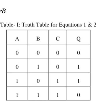
[image:1.595.321.528.635.707.2]Feynman Gate: The below given figure 1 shows the schematic arrangement of Feynman Gate with dedicated input and output terminals. The basic use of this FG gate is in the determination of the fan-out parameter of the given circuit which is further involved in the power analysis of the circuit. For this schematic arrangement of FG gate, we have two input terminals i.e. inputs (A, B) with dedicated output terminals i.e. P & Q [11-15].
Fig. 1: Feynman Reversible Gate [16]
The equations 1 & 2 given below explain the mathematical behaviour of the FG gate which is in accordance to the operational performance as
mentioned in the truth table given in table 1.
An Innovative Low Power Reversible ALU for
Quantum Processor using QCA
P
A
(1) [image:2.595.85.251.77.252.2]Q
AorB
(2)Table- I: Truth Table for Equations 1 & 2
A B C Q
0 0 0 0
0 1 0 1
1 0 1 1
1 1 1 0
[image:2.595.310.545.274.370.2]Fredkin Gate: The below given figure 2 shows the schematic arrangement of a typical Fredkin Gate with the specific input and output combinations i.e. a 3x3 reversible gate with three input and out terminals with one to one mapping. The input terminals of the FG gate are (A, B, C) which are mapped to the individual outputs which are explained with the help of the mathematical equations with the most desired features of QC as 5 using two dotted rectangles [17-19].
Fig. 2. Fredkin Reversible Gate [20].
Table- II: Truth Table for Fredkin Gate
Inputs Outputs
A B C P Q R
0 0 0 0 0 0
0 0 1 0 0 1
0 1 0 0 1 0
0 1 1 0 1 1
1 0 0 1 0 0
1 0 1 1 1 0
1 1 0 1 0 1
1 1 1 1 1 1
HNG Gate: The HNG reversible Gate is the most commonly used in the design and implementation of the various ALU for the quantum processors and can be determined in different configurations i.e. either 4x4 or 5x5. It means that this gate can have specific output terminals with dedicated inputs. Another important as aspect of this gate is the low cost and optimized delay of the transmission of the data at the output terminals. The mathematical derivation of the equations discussing the various input and output
combinations of the HNG Gate are given with the help of the equations 3 to 6 i.e. [21]
P
A
(3)Q
B
(4)
R
A
B
C
(5)
.
S
A
B C
AB
D
(6)The QC and delay calculated for HNG Gate with the use of reversible logic is 6. Now when a Boolean low logic i.e. D = 0 is applied at the input terminal, the operational behaviour of the gate provides the desired output at specific terminal i.e. R & S [22].
Fig. 3: HNG Reversible Gate [23]
[image:2.595.81.267.401.482.2]The power analysis of the of the reversible gates used for the design of the ALU for quantum processor can be determined on the basis of the behaviour specic to each input and output combinations i.e. as shown in Table 3, Table 4 and Table 5. From these Truth Tables, one can easily access each input combination with all the probable output behaviour. It has been seen that the most important condition required for a highly efficient circuit of reversible gate is that the number of input and output terminals of the gate should be optimised properly in terms of ancillae and garbage line of the gate. On this pattern, the desired parameter i.e. quantum cost of the circuit can be evaluated which in turns forms the basis of obtaining an equivalent circuit of reversible logic in terms of quantum. The below given Table 3 provides the desired information related to the quantum cost for the most commonly used reversible gates i.e. FG & HNG gates [24-26].
Table- III: Quantum Cost for FG & HNG Gates No of Control
Lines
Quantum Cost of FG Gate
Quantum Cost of HNG Gate
0 1 3
1 1 7
[image:2.595.82.256.506.666.2]Table- IV: Truth Table for HNG Gate
A B C D P Q R S
0 0 0 0 0 0 0 0
0 0 0 1 0 0 0 1
0 0 1 0 0 0 1 0
0 0 1 1 0 0 1 1
0 1 0 0 0 1 1 0
0 1 0 1 0 1 1 1
0 1 1 0 0 1 0 1
0 1 1 1 0 1 0 0
1 0 0 0 1 1 1 0
1 0 0 1 1 1 1 1
1 0 1 0 1 1 0 1
1 0 1 1 1 1 0 0
1 1 0 0 1 0 0 1
1 1 0 1 1 0 0 0
1 1 1 0 1 0 1 1
1 1 1 1 1 0 1 0
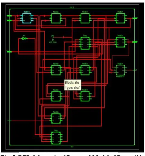
[image:3.595.298.546.84.280.2]III. PROPOSEDDESIGN&IMPLEMENTATIONOF REVERSIBLEALU
Fig. 4. Schematic diagram of proposed model of Reversible ALU.
The figure 4 shows the schematic diagram of the proposed ALU whose performance has been evaluated on the basis of the reversible logic. For this circuit, we have used the combination of the FG as well as HNG gates which are quite popular in use because of their desired performance in terms of power consumption, size and delay. This circuit has been designed and implemented using QCA tool so as to perform the basic operations which are quite common in use for a specific given ALU i.e. 8 operations as mentioned below:
From the above table we can observe that value of S2 decides what type of operation the ALU is supposed to perform: Arithmetic or Logical.
Table- V: Truth Table for the Proposed Reversible ALU
Control Inputs Operations
S0 S1 S2
0 0 0 XOR
0 0 1 XNOR
0 1 0 AND
0 1 1 OR
1 0 0 INCREMENT
1 0 1 DECREMENT
1 1 0 ADD
1 1 1 SUBTRACT
Table- VI: Truth Table for S2 of ALU
S2 Operations
0 Logical
1 Arithmetic
The whole model is dependent on the control inputs S0, S1 and S2. With the interconnection of muxes and a full adder we have obtained a design for an ALU. Here the Fredkin gate acts as a mux whereas HNG gate acts as a full adder.The diagram given below is shows the circuit connections for the ALU implemented in reversible logic.
[image:3.595.46.289.302.609.2]The outputs of the circuit are OUT and COUT respectively. COUT is given as feedback to the input to carry the ripple effect. The above circuit has been implemented using Verilog HDL. Then the output waveforms have been obtained by simulating it in XILINX. The RTL schematic obtained after simulation is given below:
Fig. 5. RTL Schematic of Proposed Model of Reversible ALU
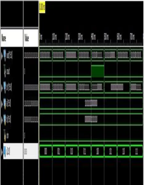
[image:3.595.307.546.430.686.2].Fig. 6. Simulation Waveform of Proposed Model of Reversible ALU
Fig. 7. Simulation Waveform for Power of Proposed Model of Reversible ALU
The above figures 6 & 7 have been obtained as the simulation results for the proposed model on the basis of the delay and power consumption by using the Xilinx software tool.
IV. COMPARATIVEANALYSISOF
CONVENTIONAL&TRADITIONALREVERSIBLE ALUDESIGN
Delay Parameter: On simulating both designs in Xilinx we got a certain delay value of each model. This delay is nothing but the time required for generation of the output on applying the input.
[image:4.595.49.289.388.714.2]Fig. 8. Delay Calculation for conventional logic
Fig. 9. Delay Calculation for reversible logic
From the given diagrams we can observe that Conventional logic produces a delay of 10.511ns whereas Reversible logic produces a delay of 7.303ns. Thus we can say that use of reversible logic has produced a significant decrease in delay for this model of an ALU.
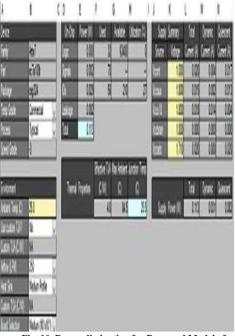
[image:4.595.318.538.394.603.2]In this process of power calculation, the signal rate of the input plays a dominant role which is nothing but defined as the rate of change of signal for the specified time period which proves to be a quite critical parameter in the determination of the power losses and consumption by the circuit. This parameter of the circuit can be easily categorized as static (standby) power and dynamic (active) power i.e. the components of the power dissipated or used in the state of power up as well as active state of the operation of the proposed reversible ALU as shown in below fig 10..
[image:5.595.299.556.47.183.2]From the given diagrams we can observe that Conventional logic produces a delay of 10.511ns whereas Reversible logic produces a delay of 7.303ns. Thus we can say that use of reversible logic has produced a significant decrease in delay for this model of an ALU.
Fig. 10. Power dissipation for Proposed Model of Reversible
The below table 9 shows the comparative analysis of the proposed circuit with the existing techniques. This comparison has been made on the basis of the various important parameters of the circuit i.e. Gate Count, Quantum Cost, Transistor Cost, Garbage output, Constant input and Line input. On the basis of the above results, it has been found that the proposed design is quite efficient and accurate since all the obtained result is quite less than the existing one which is quite desired in the design of the quantum processors.
Table- VII: Comparative Analysis of the Parameters Proposed
Analysis [09]
Existing [05]
Existing [07]
Existing [09]
Gate Count
9 (19%) 11 22 10
Quantum 21 (15%) 31 53 29
Cost Transistor Cost
0 120 - -
Garbage Output
1(87.5%) 2 12 8
Constant Input
2 (50%) 1 10 4
Line Output
6 5 - -
V. CONCLUSION
In this discussion, the author has put forward the power analysis performance analysis of a 8-functioned Arithmetic Logic Unit(ALU) in reversible logic used for the quantum processor. It shows the comparison of reversible logic based ALU with its conventional logic counterpart in terms of power consumption, dissipation, size, delay, etc. These parameters have been simulated using the QCA tool and compared with the previous works done. In this work, the author has further extended this discussion to design a more accurate & power efficient processors using the reversible technology. This discussion has been concluded by the author on the basis of the comparative analysis between the various predominant parameters of the proposed ALU as shown in Table 7.
ACKNOWLEDGMENT
The author is thankful to Hon’ble C-VI (Additional President, RBEF and Chairman AUUP, Lucknow Campus), Maj. Gen. K. K. Ohri, AVSM, Retd. (Ex-Pro VC), Amity University, Lucknow Campus, Prof. (Dr.) Sunil Dhaneshwar, Officiating Pro-V.C. Amity University, Lucknow Campus, Prof (Dr.) Ankur Gupta, Director, MIET Jammu, Wg. Cdr. Dr. Anil Kumar, Retd. (Director, ASET), and Prof. Preeta Sharan, Professor & Co-Guide, The Oxford College of Engineering, Bangalore for their support in carrying out the research work efficiently.
REFERENCES
1. Rajinder Tiwari, Deepika Bastawade, Preeta Sharan, Anil Kumar, “Performance Analysis of Reversible ALU in QCA” Indian Journal of Science & Technology, vol: 10(29), pp: 01-05, 2017.
2. Rajinder Tiwari, Anil Kumar, Preeta Sharan “Design and Implementation of 4:1 Multiplexer for Reversible ALU using QCA” published in the proceeding of 2nd International Conference Microelectronics and Telecommunication Engineering (ICMETE 2018), ISBN No: 978-1-5386-6918-1 PP No: 191-196. 978-1-5386-6918-1/18/$31.00 ©2018 IEEE
3. Arighna Sarkar and Debarka Mukhopadhyay “Improved Quantum Dot Cellular Automata 4:1 Multiplexer Circuit Unit” SOP Transactions on Nano-Technology, Vol 01, No 01, May 2104.
4. D. MUKHOPADHYAY AND P. DUTTA, “QCA BASED NOVEL UNIT
REVERSIBLE MULTIPLEXER,”ADV.SCI.LETT, VOL.5, PP.1–6,2012.
5. SAURABH KOTIYAL, HIMANSHU THAPLIYAL AND NAGARAJAN
RANGANATHAN,“MACH-ZEHNDER INTERFEROMETER BASED DESIGN
OF ALL OPTICAL REVERSIBLE BINARY ADDER”2012IEEE.
6. D. MUKHOPADHYAY,S. DINDA, AND P.DUTTA,“DESIGNING AND
IMPLEMENTATION OF QUANTUM CELLULAR AUTOMATA 2: 1
MULTIPLEXER CIRCUIT.” INTERNATIONAL JOURNAL OF COMPUTER
[image:5.595.49.289.238.581.2]7. E.GANESH AND V.KRISHNAN,“STUDY AND IMPLEMENTATION OF MUX
BASED FPGA IN QCATECHNOLOGY,”INTERNATIONAL JOURNAL OF
DISTRIBUTED AND PARALLEL SYSTEMS, VOL.2, NO.3,2011. 8. Roohi, H. Khademol hosseini, S. Sayed salehi, and K. Navi, “A novel
architecture for quantum-dot cellular automata multiplexer.” International Journal of Computer Science Issues (IJCSI), vol. 8, no. 6, 2011.
9. Y. SYAMALA, A. V. N. TILAK, “REVERSIBLE ARITHMETIC LOGIC
UNIT”,2011IEEE.
10. MATTHEW MORRISON,MATTHEW LEWANDOWSKI,RICHARD MEANA
AND NAGARAJAN RANGANATHAN,“DESIGN OF A NOVEL REVERSIBLE
ALU USING AN ENHANCED CARRY LOOK-AHEAD ADDER”,201111TH
IEEE INTERNATIONAL CONFERENCE ON NANOTECHNOLOGY
PORTLAND MARRIOTT AUGUST 15-18, 2011, PORTLAND,OREGON,
USA
11. R.FARAZKISH,M.R.AZGHADI,K.NAVI, AND M.HAGHPARAST,“NEW
METHOD FOR DECREASING THE NUMBER OF QUANTUM DOT CELLS IN QCA CIRCUITS,” WORLD APPLIED SCIENCES JOURNAL, VOL. 6, PP. 793–802,2008.
12. VANKAMAMIDI,M.OTTAVI, AND F.LOMBARDI,“TWO-DIMENSIONAL
SCHEMES FOR CLOCKING/TIMING OF QCA CIRCUITS,”COMPUTER-AIDED
DESIGN OF INTEGRATED CIRCUITS AND SYSTEMS, IEEE
TRANSACTIONS ON, VOL.27, NO.1, PP.34–44,2008.
13. M. HAGHPARAST, S. J. JASSBI, K. NAVI AND O.
HASHEMIPOUR,“DESIGN OF A NOVEL REVERSIBLE MULTIPLIER
CIRCUIT USING HNGGATE IN NANOTECHNOLOGY ”,WORLD APPLIED
SCI.J.,VOL.3, PP.974-978,2008.
14. T.R.RAKSHITH,RAKSHITH SALIGRAM."DESIGN OF HIGH SPEED LOW
POWER MULTIPLIER USING REVERSIBLE LOGIC: A VEDIC
MATHEMATICAL APPROACH",2013INTERNATIONAL CONFERENCE ON
CIRCUITS,POWER AND COMPUTING TECHNOLOGIES (ICCPCT),2013
15. ANKITA TIWARI,RAJINDER TIWARI."DESIGN OF A BRAIN COMPUTER
INTERFACE FOR STRESS REMOVAL USING YOGA A SMARTPHONE
APPLICATION",2017INTERNATIONAL CONFERENCE ON COMPUTING,
COMMUNICATION AND AUTOMATION (ICCCA),2017
16. JEFERSON F.CHAVES,DOUGLAS S.SILVA,VICTOR V.CAMARGOS AND
OMAR P.VILELA NETO “TOWARDS REVERSIBLE QCA COMPUTERS:
REVERSIBLE GATES AND ALU”
17. ”DESIGN OF MULTIPLEXER BASED 64-BIT SRAM USING QCA”-K.
PANDIAMMAL AND D.MEGANATHAN
18. “BASIC REVERSIBLE LOGIC GATES AND IT’S QCA IMPLEMENTATION”, PAPIYA BISWAS,NAMIT GUPTA,NILESH PATIDAR
19. “INTRODUCTION TO REVERSIBLE LOGIC GATES AND ITS APPLICATION”,
PRASHANT Y,PROF.SUJATA
20. “ZERO POWER QUANTUM GATES FOR THE IMPLEMENTATION OF
REVERSIBLE LOGIC CIRCUITS FOR A QUANTUM
COMPUTER”-SAMYUKTA HASSAN,DR.PREETA SHARAN,DR.SRINIVAS T
21. ” A NEW REVERSIBLE TSG GATE AND ITS APPLICATION FOR
DESIGNING EFFICIENT ADDER CIRCUITS”. THAPLIYAL H, M. B.S
SHRINIVAS. CENTRE FOR VLSI AND EMBEDDED SYSTEM
TECHNOLOGIES INTERNATIONAL INSTITUTE OF INFORMATION
TECHNOLOGY,HYDERABAD,500019,INDIA
22. “DESIGN OF REVERSIBLE LATCHES OPTIMIZED FOR QUANTUM COST,
DELAY AND GARBAGE OUTPUTS”,THAPLIYAL H,RANGANATHAN N.”
23. P. SAI PHANEENDRA, CHETAN VUDADHA, V.SREEHARI, M.B.
SRINIVAS. AN OPTIMIZED DESIGN OF REVERSIBLE QUANTUM
COMPARATOR",201427TH INTERNATIONAL CONFERENCE ON VLSI
DESIGN AND 201413TH INTERNATIONAL CONFERENCE ON EMBEDDED
SYSTEMS,2014
24. MATTHEW MORRISON,NAGARAJAN RANGANATHAN."DESIGN OF A
REVERSIBLE ALUBASED ON NOVEL PROGRAMMABLE REVERSIBLE
LOGIC GATE STRUCTURES",2011IEEECOMPUTER SOCIETY ANNUAL
SYMPOSIUM ON VLSI,2011
25. SARAVANAN,P., AND P.KALPANA."A NOVEL APPROACH TO DESIGN
A5/1 STREAM CIPHER USING POWER ANALYSIS ATTACK RESISTANT
REVERSIBLE LOGIC GATES",INTERNATIONAL JOURNAL OF ENTERPRISE
NETWORK MANAGEMENT,2016.
26. P.GOWTHAMI,R.V.S.SATYANARAYANA."DESIGN OF AN EFFICIENT
MULTIPLIER USING VEDIC MATHEMATICS AND REVERSIBLE LOGIC",
2016 IEEE INTERNATIONAL CONFERENCE ON COMPUTATIONAL
INTELLIGENCE AND COMPUTING RESEARCH (ICCIC),2016
AUTHORSPROFILE
Rajinder Tiwari, Presently, associated with Department of ECE, MIET, Jammu in the capacity of Assoc. Professor from Feb, 2018 to till dated. He has got an experience of about 16+ years in the domain of academics, research and industry. He is also pursuing the Doctorate of Philosophy (PhD) in ECE from Department of ECE, ASET, Amity University, Uttar Pradesh from 2017 – 2021 (Batch) on the topic “Performance & Comparative Analysis of Quantum based Processor with CMOS Technology”. He has published about 35 research papers in Journals and Conferences of high repute i.e. SCOPUS/SCI/IEEE indexed. He is also associated with many International Journals as Reviewer & Editorial Members with reputed publishers i.e. IEEE, IETE, SCOPUS, SCI Indexed Publications. He has also delivered invited lectures in the domain of CMOS VLSI design and Quantum Computing. Mr. Tiwari is a senior & lifetime member of various bodies such as IAEng, IETE, IET (U.K.), MRSI, & UACEEE.
Vikas Rajiv is student pursuing his UG degree course from Dept of ECE, The Oxford College of Engineering, Bengaluru, India. His filed of interest is the simulation of the various digital circuits using QCA & Verilog tool.
.
Dr. Preeta Sharan is working as professor in the department of ECE, The Oxford College of Engineering, India. She did her Post-Doctoral, Indian Institute of Technology (IIT), Kharagpur and did her PhD degree in ECE, Institute of Technology (IT), BHU, India. The main focus of her research is related with photonics and optoelectronics. A competent professor with 22+ years of experience in Education, Research, Student Mentorship, association with international universities and organizations. Responsible for teaching B.Tech/ M.Tech. Guide Phd. students and execute government/ international agency funded projects. A self-starter with strong entrepreneurial spirit, built R&D center of my own with team size 15+ from scratch. I have delivered projects for prestigious funding agencies across the world as lead investigator like Naval Research Board, DRDO, India, IEEE USA and Govt. of Karnataka (KVGST). With multiple patents in process, research publications reaching 100+ under my leadership. Visited facilities of leading universities NTU Singapore,
![Fig. 1: Feynman Reversible Gate [16]](https://thumb-us.123doks.com/thumbv2/123dok_us/8166754.251164/1.595.321.528.635.707/fig-feynman-reversible-gate.webp)