White Rose Research Online URL for this paper:
http://eprints.whiterose.ac.uk/80230/
Version: Accepted Version
Article:
Brydson, R, Brown, A, Benning, LG et al. (1 more author) (2014) Analytical transmission
electron microscopy. Reviews in Mineralogy and Geochemistry, 78 (1). 219 - 269. ISSN
1529-6466
https://doi.org/10.2138/rmg.2014.78.6
[email protected] https://eprints.whiterose.ac.uk/ Reuse
Unless indicated otherwise, fulltext items are protected by copyright with all rights reserved. The copyright exception in section 29 of the Copyright, Designs and Patents Act 1988 allows the making of a single copy solely for the purpose of non-commercial research or private study within the limits of fair dealing. The publisher or other rights-holder may allow further reproduction and re-use of this version - refer to the White Rose Research Online record for this item. Where records identify the publisher as the copyright holder, users can verify any specific terms of use on the publisher’s website.
Takedown
If you consider content in White Rose Research Online to be in breach of UK law, please notify us by
Copyright © Mineralogical Society of America
1529-6466/13/0078-0006$10.00 http://dx.doi.org/10.2138/rmg.2013.78.6
Analytical Transmission Electron Microscopy
Rik Brydson
1, Andy Brown
1, Liane G. Benning
2 1Institute for Materials Research2School of Earth and Environment University of Leeds Leeds, LS2 9JT, United Kingdom
Ken Livi
High-Resolution Analytical Electron Microbeam Facility Integrated Imaging Center
Department of Earth and Planetary Sciences Johns Hopkins University
Baltimore, Maryland 21218, U.S.A.
INTRODUCTION
Analytical transmission electron microscopy (TEM) is used to reveal sub-micrometer, internal ine structure (the microstructure or ultrastructure) and chemistry in minerals. The
amount and scale of the information which can be extracted by TEM depends critically on four parameters; the resolving power of the microscope (usually smaller than 0.3 nm); the energy spread of the electron beam (of the order of an electron volt, eV); the thickness of the specimen (almost always signiicantly less than 1 mm), and the composition and stability of the specimen. An introductory text on all types of electron microscopy is provided by Goodhew et al. (2001), while more detailed information on transmission electron microscopy may be found in the comprehensive text of Williams and Carter (2009).
INTRODUCTION TO ANALYTICAL TRANSMISSION ELECTRON MICROSCOPY (TEM)
Basic design of transmission electron microscopes (TEM)
The two available modes of TEM—CTEM and STEM—differ principally in the way they address the specimen. Conventional TEM (CTEM) is a wide-beam technique, in which a close-to-parallel electron beam loods the whole area of interest and the image (or diffraction pattern), formed by an imaging (objective) lens after the thin specimen from perhaps 106-107 pixels on a digital camera, is collected in parallel. Scanning TEM (STEM) deploys a ine focused beam, formed by a probe-forming lens before the thin specimen, to address each pixel (here, a dwell point) in series and form a sequential image as the probe is scanned across the specimen. Figures 1 and 2 summarize these different instrument designs; here it should be noted that many modern TEM instruments are capable of operating in both modes, rather than being instruments dedicated to one mode of operation.
specimen within which various elastic and inelastic scattering (energy-loss) processes take place.
In both CTEM and STEM, electrons are produced from an electron emitter, focused and collimated into a beam and inally accelerated to a given beam energy. Key instrumental com-ponents, which affect the microscope resolution and analytical performance, are:
• the electron emitter which can operate via either a thermionic or ield emission mechanism or a combination of the two; ield emission provides the brightest, most monochromatic and coherent source of electrons.
• the accelerating voltage (Eo, typically in the range 60-300 kV) and hence incident electron energy; the higher the accelerating voltage the higher the resolution and the larger the sample penetration (although, in certain cases depending on the elements present and their chemical bonding, sample damage via sputtering may be an issue above a certain threshold energy).
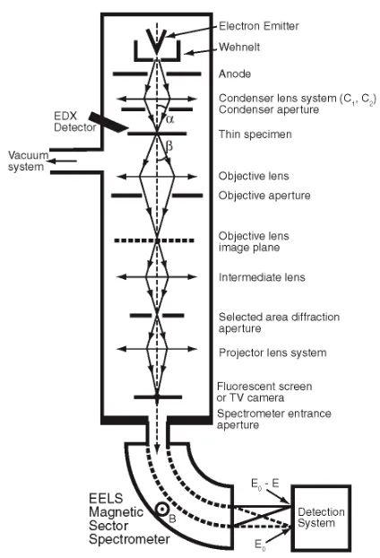
[image:3.474.117.329.74.385.2]In the CTEM (Fig. 1), two or more electromagnetic condenser lenses demagnify the probe to a size typically between a few micrometers and a few nanometers—the excitation of these lenses controls both the beam diameter and the beam divergence/convergence angle. For these
Figure 1. Schematic diagram of the layout of an analytical conventional transmission electron microscope
condenser-lens systems the irst condenser (C1 or spot size) controls the demagniication of the source, while the second (C2 or intensity) controls the size of the spot at the specimen and hence the beam divergence/convergence.
The specimen is in the form of a thin (< 100 nm) 3 mm diameter disc of either the material itself or the material supported on an electron transparent ilm. The specimen is usually inserted into the vacuum of the TEM via an airlock and ixed into a side-entry specimen rod that can be translated or tilted (about one or two axes).
[image:4.474.155.345.76.256.2]In the CTEM (see Fig. 1), the main electromagnetic objective lens forms the irst intermediate, real space, projection image of the illuminated specimen area (in the image plane of the lens) as well as the corresponding reciprocal space diffraction pattern (in the back focal plane of the lens). Here the image magniication relative to the specimen is typically 50-100 times. For a given electron emitter and accelerating voltage, the image resolution in CTEM is principally determined by imperfections or aberrations in this objective lens. An objective aperture can be inserted in the back focal plane of the objective lens to limit beam divergence in reciprocal space of the transmitted electrons contributing to the magniied image. Typically there are a number of circular objective apertures ranging from 10 to 100 mm in diameter. The projector lens system consists of a irst projector or intermediate lens that focuses on either the objective lens image plane (microscope operating in imaging mode) or the back focal plane (microscope in diffraction mode). The irst projector lens is followed by a series of three or four further projector lenses—each of which magnify the image or diffraction pattern by typically up to 20 times. The Selected Area Electron Diffraction (SAED) aperture usually lies in the image plane of one of the projector lenses (due to space considerations) and if projected back to the irst intermediate image and hence the specimen effectively allows the selection of a much smaller area (typically ranging from a few tenths of a micron to a few microns) on the specimen for the purposes of forming a diffraction pattern. The overall microscope system can provide a total magniication of up to a few million times on the electron luorescent microscope
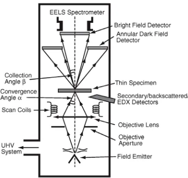
Figure 2. Schematic diagram of the layout of a dedicated analytical scanning transmission electron
viewing screen or, below this, the camera (either a photographic plate or a phosphor coupled to a two dimensional charge coupled diode (CCD) array).
In the STEM (see Fig. 2), as opposed to CTEM, there is usually only a condenser lens system, which is better called a probe-forming lens; confusingly in a STEM this is often referred to as an objective lens—however, the important distinction from the case of CTEM is that this objective lens lies before the specimen. This lens system is used to form a small diameter (typically a nanometer or less) probe that is serially scanned in a two-dimensional raster across the specimen. At each point the transmitted beam intensity is measured—thus building up a serial image of the specimen. Two intensities are usually recorded: that falling on an on-axis bright ield (BF) detector that collects electrons that have undergone relatively small angles of scattering (principally undiffracted, Bragg diffracted and inelastically scattered electrons which gives images equivalent to CTEM BF images), as well as that incident on a high-angle annular dark-ield (HAADF) detector that principally collects higher-angle (beyond the diffracted spots) incoherently elastically scattered electrons (so called Z-contrast images). In a STEM instrument, the resolution of the scanned image (as well as the analytical resolution described above) is determined largely by the beam diameter generated by the probe-forming lens and this is also limited by lens aberrations. As discussed in the introduction, there are now many hybrid CTEM/STEM instruments, which can operate in both modes.
Interactions between the electron beam and the specimen
The high-energy incident electron beam of the TEM interacts with the sample in a number of ways. Low-angle, coherent elastic scattering (diffraction) of electrons (through 1°-10°) occurs via the interaction of the incident electrons with the electron cloud associated with atoms in a solid—this is used for CTEM and STEM bright ield imaging. High-angle, incoherent elastic (back)scattering (through 10-180°) occurs via interaction of the negatively charged electrons with the nuclei of atoms—this is used for STEM dark ield imaging. The cross section or probability for elastic scattering varies roughly as the square of the mean atomic number of the sample, whereas inelastic scattering, which provides the analytical signal, generally involves much smaller scattering angles than is the case for elastic scattering; the cross section of inelastic scattering varies linearly with atomic number.
Inelastic scattering of electrons by solids predominantly occurs via four major mechanisms: 1. Phonon scattering, where the incident electrons excite phonons (atomic vibrations)
in the material. Typically the energy loss is < 1 eV, the scattering angle is quite large (∼10°) and for carbon, the average distance between such scattering events—the mean free path, Λ—is ∼1 mm. This is the basis for heating of the specimen by an electron beam.
2. Plasmon scattering, where the incident electrons excite collective, ‘‘resonant’’
oscilla-tions (plasmons) of the valence (bonding) electrons associated with a solid. Here, the energy loss from the incident beam is between 5-30 eV and Λ is ∼100 nm, causing this to be the dominant scattering process in electron-solid interactions.
3. Single-electron excitation, where the incident electron transfers energy to single atom-ic electrons resulting in the ionization of atoms. The mean free path for this event is of the order of mm. Lightly bound valence electrons may be ejected from atoms and, if they escape from the specimen surface, may be used to form secondary electron images in scanning electron microscopy (SEM). Energy losses for such excitations typically range up to 50 eV. If inner-shell electrons are removed, the energy loss can be up to keV. For example, the energy loss required to ionize carbon 1s (i.e., K shell)
also be used for analytical purposes in the techniques of either energy dispersive or wavelength dispersive X-ray (EDX/WDX) spectroscopy.
4. Direct radiation losses, the principal of which is Bremsstrahlung X-ray emission caused by the deceleration of electrons by the solid; this forms the background in the X-ray emission spectrum upon which are superimposed characteristic X-ray peaks produced by single-electron excitation and subsequent relaxation. The Bremsstrah-lung energy losses can take any value and can approach the total incident beam en-ergy in the limit of full deceleration.
Brief review of imaging mechanisms in CTEM and STEM. All TEM images are two
dimensional projections of the internal structure of a thin specimen region. In recent years, however, there has been considerable interest in reconstructing the three dimensional nature of the specimen using tomographic techniques (see Weyland and Midgley (2007) in Hutchison
[image:6.474.105.392.85.427.2]
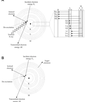
Figure 3. Energy dispersive X-ray analysis in the TEM (after Brydson 2011). De-excitation mechanisms
for an atom which has undergone K-shell ionization by primary electrons: (A) emission of a characteristic Kα X-ray (the inset details possible ionization processes and emission of X-rays) and (B) emission of a KLM Auger electron.
A
and Kirkland (2007)). Notwithstanding, unless they are STEM EDX or EEL spectrum images or energy iltered CTEM images (see “EDX and EELS Imaging” section below), all TEM
images are based principally on the elastically scattered components of the incident electron beam although the images may contain some underlying inelastically scattered contribution (Williams and Carter 2009).
There are three basic contrast mechanisms which contribute to all CTEM images: 1. Mass-thickness contrast: sample regions (whether amorphous or crystalline) that are
thicker or of higher density will scatter the electrons more strongly and hence more electrons will be scattered through high angles and be lost in their passage down the narrow bore of the microscope column so making these areas appear darker in the im-age.
2. Diffraction contrast: crystalline regions of the sample oriented at the Bragg angle for
diffraction will excite diffracted beams, which correspondingly reduce the amplitude of the unscattered beam. Insertion of an objective aperture in the back focal plane can accentuate this effect via formation of bright ield (BF) images (the unscattered beam selected with diffracting regions appearing dark) or dark ield (DF) images (a diffracted beam selected, with diffracting regions appearing bright). Any microstruc-tural feature which changes the corresponding diffraction condition (such as a grain boundary, stacking fault, strain ield or a line defect etc.) will, in principle, show up in diffraction contrast.
3. Phase contrast: this relies on the interference between the unscattered beam and
dif-ferent diffracted beams to produce an interference pattern (visible at high magniica-tion) which relects the lattice periodicity; effectively lattice planes and hence atomic positions are imaged but may appear light or dark depending on the microscope condi-tions (objective lens defocus, beam energy etc.) and the sample thickness.
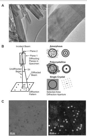
Some examples of these three CTEM contrast mechanisms are given in Figure 4A as well as in many subsequent igures in the chapter. In addition to imaging, as discussed in the Introduction, the diffraction pattern in the back focal plane may be viewed. The area of the specimen from which the diffraction pattern originates can be deined using the SAED aperture (using effectively parallel illumination) or the probe can be converged to a small area on the specimen so as to form diffraction discs (whose radius depends on the convergence angle) rather than spots. The diffraction pattern allows the degree of crystallinity as well as the exact crystallographic phase of the material to be determined as well as the incident beam direction through the crystal. See Figure 4B for a schematic diagram and also Figures 16 and 19 for an example diffraction patterns.
STEM bright ield images contain all the same contrast mechanisms as CTEM bright ield images, whereas STEM dark ield images (particularly HAADF which relies on Rutherford scattering from the nuclei) images are relatively insensitive to structure and orientation but strongly dependent on atomic number (Z contrast), with the intensity varying as Zζ where ζ
lies between 1.5 and 2. If the specimen is uniformly thick in the area of interest the HAADF intensity can be directly related to the average atomic number in the column at each pixel. Figure 4C shows an example BF and DF STEM image. If the beam is less than one atom dimension in diameter, for instance in an aberration-corrected STEM (see later), then atom column compositional resolution is therefore possible (strictly, only if we have strong channeling of the probe down the atomic columns which occurs when the sample is oriented along a low Miller index zone axis).
Figure 4. (A) TEM bright ield image of a tubular halloysite clay mineral showing both CTEM mass
thick-ness contrast (from the amorphous carbon support ilm and the halloysite tubes) and CTEM diffraction con-trast from some of the halloysite tubes oriented at the Bragg angle for diffraction. At higher magniication CTEM phase contrast is evident in the (002) basal plane lattice fringes of tube walls (Brydson and Hillier, unpublished). (B) Schematic diagram of the geometry of electron diffraction in the CTEM and the form of the selected area diffraction pattern for amorphous, polycrystalline and single crystal sample regions. Examples of real diffraction patterns are shown in Figure 16 and subsequent igures. (C) Example of (left) a STEM BF image and (right) a STEM high angle annular dark ield image from a cluster of iron storage proteins, ferritin molecule mineral-cores (doped ferrihydrite) cores within a tissue section (see Pan et al. 2009).
Figure 4A
A
C
transmission electron microscope are both concerned with inelastic interactions and are based on the analysis of either the energy or wavelength of the emitted X-rays (EDX or WDX), or the direct energy losses of the incident electrons (EELS).
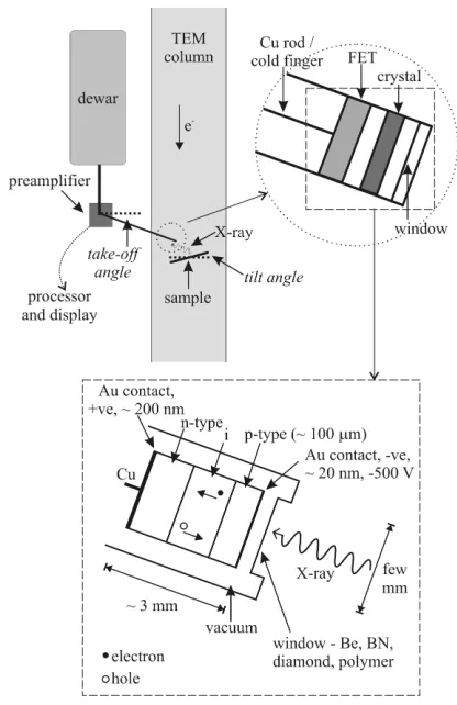
[image:9.474.117.325.290.611.2]As shown in Figure 5, X-rays produced when the electron probe interacts with the specimen are most commonly detected from the incident surface using a low take-off angle Energy Dispersive X-ray (EDX) detector (i.e., the detector is approximately in the same plane as the sample, some 20° to the horizontal), so as to allow the detector to be brought close to the sample and also to minimize the predominantly forward-peaked Bremsstrahlung background contribution to the X-ray emission spectrum. Even though the detector is inserted to within a few mm of the sample surface, it collects only a small proportion (usually only a few percent) of the isotropically emitted X-ray signal owing to the limited solid collection angle of the detector (typically signiicantly less than 1 Steradian, from a total possible solid angle of 4π Steradians). Generally, the specimen is tilted towards the detector (typically through ca. 15°) so as to provide a clear X-ray trajectory between the irradiated area and the detector. The volume of the specimen that produces X-rays is controlled by the electron probe size (and hence condenser-lens currents) as well as beam broadening within the specimen that increases with (among other things) thickness and average atomic number and decreases with
Figure 5. Energy dispersive X-ray analysis in the TEM (after Brydson 2011). Schematic diagram showing
microscope accelerating voltage. High take-off angle X-ray detectors also exist and these do not require the specimen to be tilted towards the detector.
Below the microscope viewing screen, the self-contained EELS spectrometer (which almost always possesses a variable entrance aperture itself) and detection system collects the transmitted electron signal that is composed of both elastically and inelastically scattered electrons. In both Figures 1 and 2, α and β are known as the convergence and collection semi-angles, respectively. Note certain commercial EELS systems (particularly those initially developed for the purposes of energy-iltered imaging) employ an in-column design with the EEL spectrometer placed between the objective and projector lenses. Further details are given in the “EDX and EELS Imaging” section below.
As discussed in the introduction, apart from the case of energy iltered CTEM (see “EDX and EELS Imaging” section below), analytical information is most usually collected using a
focused probe. In this respect STEMs are ideal analytical machines since they easily allow the simultaneous recording of images and X-ray emission spectra, furthermore retraction of the bright-ield detector allows electrons to enter an EEL spectrometer while still simultaneously recording the HAADF image. Generally, STEMs can collect analytical EDX and EELS data in one of two ways: irstly, by scanning the beam over an area and collecting the signal from the whole scanned area and, secondly, by scanning the beam slowly and recording the analytical signal serially at each point (known as spectrum imaging). Dedicated STEMs employ extremely small probe sizes produced by cold ield-emission electron sources that can provide extremely high energy resolution (EELS) and high spatial resolution (EELS and EDX) measurements.
The specimen
A specimen suitable for study by analytical TEM should be thin enough for electron transmission without signiicant spreading of the electron beam, yet be representative of the material about which we wish to draw conclusions. These simple requirements imply that in most cases we must prepare a thin specimen (typically less than 50 nm for high resolution studies) from a larger sample, and in all cases we must assure ourselves that the processes of preparation, mounting and examination do not change, in any uncontrolled way, the important features of the specimen. Specimen preparation is therefore an absolutely crucial aspect of analytical TEM. This is discussed in the “Example of the practical application of EDX: clay minerals – Sample preparation” and “Developments in TEM specimen preparation” sections
below. However, for the vast majority of mineralogical and geological samples this usually involves cleaving or crushing a sample in an agate mortar and pestle, dispersing in a suitable inert liquid and drop-casting onto a TEM grid with a thin, usually amorphous and often holey support ilm. An alternative procedure, which retains the microstructural relationships in the overall specimen, involves the thinning and polishing of a bulk 3 mm disc of material cut using a drill or ultrasonic disc cutter. Course-scale thinning of the disc is usually performed mechanically using standard polishing procedures employing silicon carbide, diamond and alumina or silica abrasives of progressively decreasing roughness. Final thinning to electron transparency (ca. 100 nm) can be achieved via either: accurate and controlled mechanical polishing (tripod polishing); chemical polishing using jets of acids or alkalis or, very commonly, ion milling using a broad low energy argon ion beam. More recently the use of focused ion beam (FIB) specimen preparation techniques, although not without their speciic problems associated with sample damage, has radically altered the preparation of thin TEM specimens from site-speciic areas within larger samples, in particular cross sections of interfaces and surfaces (see Fig. 19 and also Giannuzzi 2004).
as dose) which is dependent on the incident energy of the electron beam, the interaction cross section for the specimen, the electron luence (i.e., the total number of electrons incident per unit area of specimen) and, in some cases, the luence rate (usually quoted in current per unit area) can be important. In many cases, for a given set of microscope conditions, there is a “safe” luence or luence rate below which damage is negligible.
Beam damage of the specimen can occur by two dominant mechanisms: knock-on damage in which an atom or ion is displaced from its normal site, and ionization damage (in some contexts called radiolysis) in which electrons are perturbed leading to chemical and then possibly structural changes (Egerton et al. 2004; Williams and Carter 2009). The latter can also eventually result in specimen heating. Both types of damage are very dificult to predict or quantify with accuracy, because they depend on the bonding environment of the atoms in the specimen. In most circumstances, however, the knock-on cross section increases with primary beam energy, while the ionization cross section decreases. Thus there is a compromise to be struck for each specimen to ind a beam energy that is low enough not to cause signiicant atomic displacement but is high enough to suppress radiolysis.
Recent developments in analytical TEM
As mentioned previously, the image resolution in CTEM is primarily determined by the imperfections or aberrations in the objective lens, while in a STEM instrument the resolution of the scanned image (as well as the analytical resolution for EDX and EELS) is determined largely by the beam diameter generated by the probe-forming lens which is also limited by aberrations. In both cases the most serious lens aberration is spherical aberration, whereby electrons travelling at differing distances from the central optic axis of the lens are focused to different positions. In recent years, technical dificulties have been overcome (principally due to increases in computing power) which has allowed both the diagnosis and correction of an increasing number (and type) of these lens aberrations (Hawkes 2008). Aberration correction could in principle be applied to any magnetic lens in any microscope. In practice there are two key areas where it is employed (in some cases in tandem) to correct spherical aberration: (i) in the condenser/illumination or probe-forming system (STEM) and (ii) in the objective or imaging lens (CTEM). With the correction of spherical aberration, the next resolution-limiting lens aberration, particularly at low accelerating voltages, is chromatic aberration whereby electrons of differing energies are focused to different positions. At the time of writing there are a number of schemes being developed and implemented for chromatic aberration correction (Leary and Brydson 2011). One of the main beneits of the correction of aberrations in STEM is in the reduction of the “beam tails” so that a ine beam positioned on a speciied column of atoms does not “spill” signiicant electron intensity into neighboring columns. This has big implications for the STEM-based techniques of HAADF or “Z contrast” imaging, EELS and
EDX analysis and even tomography (Brydson 2011).
Particularly with the advent of micro-electromechanical systems (MEMS) technology, it is now becoming increasingly possible to control many environmental parameters associated with the specimen while in many cases simultaneously imaging or spectroscopically analyzing a region of interest. Possible in situ experiments that have been demonstrated include:
specimen heating or cooling, specimen straining or compression, the control of local electric or magnetic ields, measurement of local specimen conductivity, illumination of the specimen with photons, even imaging the specimen under the presence of environmental atmospheres of gas or even (lowing) liquids (see chapter by Gai (2007) in Hutchison and Kirkland (2007)).
Finally, as mentioned at the beginning of subsection “Brief review of imaging mechanisms in CTEM and STEM”, methodologies for three dimensional TEM image reconstructions
potentially akin to geology and mineralogy. In terms of analytical TEM, the basic possibilities are any signal, which monotonically increases with increasing thickness such as HAADF images and potentially EDX and EEL spectrum images or energy iltered TEM images (EFTEM) (see section below on “EDX and EELS imaging”).
ELEMENTAL QUANTIFICATION – EDX AND EELS
EDX
As discussed previously (section “Interactions between the electron beam and the specimen”), following ionization of atoms in a sample by an electron beam, one possible
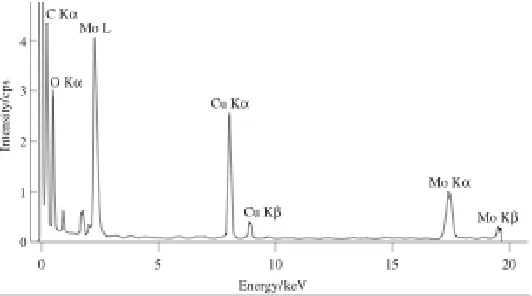
de-excitation process is X-ray emission. The energy of the X-ray photon emitted when a single outer electron drops into the inner shell hole is given by the difference between the energies of the two excited states involved. A set of dipole selection rules determines which transitions are observed and these are labeled due to a standard notation: e.g., K excitation for ionization of 1s electrons, L for 2s (L1) and 2p (actually spin orbit split into L2 for 2p1/2, L3 for 2p3/2) electrons etc. with corresponding subscripts (α, β, etc.) denoting the electron from the upper energy level which ills the ionized hole. Due to the well-deined nature of the various atomic energy levels, it is clear that the energies of the set of emitted X-rays will have characteristic values for each of the atomic species present in the specimen and by measuring these energies of the X-rays emitted from the sample, it is possible to determine which elements are present at the particular position of the electron probe. Figure 6 shows a typical electron-generated X-ray emission spectrum from Molybdenum oxide. The Mo Kα, Kβ and Lα X-ray lines as well as the O Kα line are superimposed upon the Bremsstrahlung background. The latter X-rays are not characteristic of any particular atom but depend principally on specimen thickness. To a irst approximation, peak intensities are roughly proportional to the atomic concentration of the element and, through careful measurements and comparison to elemental/mineralogical standards, EDX can detect levels of elements down to 0.1 at%. Many further example EDX spectra are given in subsequent igures.
[image:12.474.118.384.444.592.2]EDX detectors collect X-rays in a near-parallel fashion and rely on the creation of electron-hole pairs in a biased doped silicon crystal; the number of electron-hole pairs and hence current is directly proportional to the energy of the incident X-ray. Fast electronics allow
separate pulses of X-rays to be discriminated and measured. EDX detectors often have some form of window (either beryllium or, for a thinner more sensitive window, a polymer) which, depending on the material and thickness, may reduce sensitivity to light elements (Z < 11).
New developments in EDX detectors em-ploy silicon-drift detector (SDD) technology that have several advantages: 1) SD detectors can be designed to it closer to the sample and subtend a greater solid collection angle so col-lecting more X-rays per unit time; 2) several SDD’s can be linked in parallel to cover a sol-id collection angle approaching 1 Steradian. This requires a high level of integration of the detectors into the microscope optical design, and thus, is only available from the micro-scope manufacturer at the time of the publica-tion of this chapter; 3) SDD technology can handle large amounts of incident X-rays (105-6 counts/s), levels that would normally satu-rate the conventional Si(Li) detectors (103-4 counts/s); 4) liquid nitrogen cooling is not necessary for SDD, which are Peltier cooled. This technology is still in the early stages of implementation on the TEM and promises to improve signiicantly elemental detection lim-its and also X-ray mapping capabilities.
Compared to the alternative method of detection via X-ray wavelength (Wavelength Dispersive X-ray Spectroscopy, WDX) rather than energy EDX, EDX is cheaper to imple-ment and very fast in terms of acquisition, but it has a much poorer resolution and hence sen-sitivity to all elements, particularly light ele-ments. WDX is generally conined to dedicat-ed analytical Scanning Electron Microscopes (SEMs) known as Electron Probe Microana-lyzers (EPMA), while EDX detectors may be itted as an add-on attachment to most SEMs and TEMs.
[image:13.474.245.395.126.518.2]Practical EDX acquisition and quantii-cation. Identifying which elements are present in signiicant amounts from an EDX spectrum such as that shown in Figure 6 or Figure 7, is relatively routine. The positions and relative heights of the various X-ray peaks are either tabulated in references or, more commonly, are stored in a database associated with the software package of the EDX system. Work-ing from the high-energy end of the spec-trum, for internal consistency, it is necessary to conirm manually that if the K lines for a
particular element are present, then the corresponding L (and possibly M lines) is also evident. Pre-processing of the spectrum prior to quantiication involves both background subtraction and correction for escape peaks due to X-ray absorption in the surface of the detector and sum peaks due to the near simultaneous arrival (and hence detection) of two X-rays at high count rates. This may be performed using deconvolution techniques involving Fourier transforma-tion and iltering, or alternatively both the background and escape and sum fractransforma-tions may be modeled mathematically. Such facilities are an integral part of many currently available EDX software packages.
After the spectrum has been processed, the characteristic X-ray peaks are matched, using least squares methods, either to stored spectra or to computed proiles. Such a procedure can also deal with the problem of overlapping peaks. Alternatively, simple integration of areas under the peaks may be performed. Once the characteristic line intensities have been extracted the next step is to turn these into a chemical composition present in the irradiated sample volume. For quantiication it is necessary to know the relevant cross sections for X-ray excitation by the accelerated electrons as well as the absorption characteristics of the window, electrode and dead layer of the X-ray detector, so as to correct the measured X-ray intensities. The most usual approach to tackling this problem is to use a proportionality factor known as a k-factor; this may be calculated from irst principles or, more usually, it is measured
experimentally. The latter approach employs a standard compound of known composition that contains the elements of interest. The basic equation for the analysis of inorganic materials is:
A A
AB
B B
C I
k
C = I
where C denotes the concentration in wt% and I denotes the characteristic X-ray peak intensity
above the background, for both elements A and B. kAB is the appropriate proportionality or
k-factor, also known as a Cliff-Lorimer factor, which is independent of specimen composition
and thickness but varies with accelerating voltage. Frequently, k-factors are measured for
several element pairs that have a common element such as Si; kAB is then simply given by kAB = kASi/kBSi. EDX software packages often provide a set of k factors, obtained for a particular detector system at a given electron beam accelerating voltage, known as a virtual standards pack. If the specimen is very thin (a few tens of nanometers), it is possible to neglect the following phenomena: (i) the differing absorption, within the material itself, of the various characteristic X-rays generated in the specimen as they travel to the specimen exit surface en route to the detector, and (ii) luorescence of one characteristic X-ray by another higher-energy characteristic X-ray. If however, the specimen is thicker, or for quantiication of the concentration of a light element present in a heavy element matrix then, for accuracy, we have to correct for these effects, in particular absorption. The absorption correction employs an iterative procedure that initially assumes a starting composition for the specimen based on the uncorrected X-ray intensities. The absorption of different energy X-rays in this specimen en route to the detector is then accounted for using a Beer-Lambert-type expression to give a new composition that is subsequently used as input to a further absorption correction. This procedure is repeated until the change in composition falls below some preset level of required accuracy. Fluorescence by characteristic X-rays is only really signiicant when there are two elements of interest with similar X-ray energies and the energy of one X-ray is just above the absorption edge of another X-ray (e.g., elements close to each other in the periodic table). Fluorescence is made considerably worse by the presence of a large concentration of the luorescing element combined with a small concentration of the luoresced species.
With careful measurement and analysis, EDX can detect levels of elements down to 0.1 at% with an accuracy of roughly 5%. However, the absorption of low-energy X-rays becomes a severe problem for elements of Z < 11 and this can make light-element quantiication
In terms of element detectability using analytical TEM, two important quantities are irstly, the minimum mass fraction (MMF), which is the smallest composition (expressed
in either wt% or at%) detectable; secondly, the minimum detectable mass (MDM) is the
minimum number of atoms detectable in the analytical volume probed. Generally for analytical transmission electron microscopy, the MMF is rather poor compared to many other analytical techniques principally due to either the low total signal detected (EDX) or the large background contribution (EELS). The ability to form small, intense electron probes means that it is possible to analyze very small total sample masses and, for a given detectable MMF, this results in a low MDM, which is one of the major beneits of analytical transmission electron microscopy; aberration correction can signiicantly improve this capability (see section on “Recent developments in analytical TEM” and Brydson 2011).
When EDX is used in the TEM, the thin nature of the TEM sample (as opposed to a bulk SEM sample) leads to much reduced broadening of the electron beam during its passage through the specimen (the so-called interaction volume) and, since EDX analysis will collect all X-rays produced isotropically within the beam-broadened volume within the specimen, the elemental analysis will possess a high spatial resolution. In practice at 100 keV, a 100 nm thick sample typically gives a beam broadening of the order of a few nanometers and by generating a small focused STEM probe, EDX spectrum imaging maps can now routinely demonstrate resolutions of 5-10 nm in thin sample areas (see Fig. 7 and also Fig. 19). However, it is important to realize that the smaller you make the probe, the more you reduce the current within the probe as electrons are “lost” in the (sometimes ixed) apertures in the column; this then means that fewer X-rays are generated lowering the spectrum signal to noise ratio (SNR). Aberration corrected STEMs, can achieve ultraine electron probes with more current and very high (even atomic column) resolution EDX maps have been demonstrated, most probably at the risk of increased beam damage and hydrocarbon contamination (Brydson 2011). However, such high spatial resolution mapping requires the use of high solid angle, high throughput EDX SDDs which can signiicantly increase count rates both collected and processed by the detector. This has signiicantly enhanced EDX spectrum imaging capabilities both in terms of acquisition times and spatial resolution.
Below we outline the major issues associated with the practical application of TEM/EDX in mineralogical research.
Example of the practical application of EDX: clay minerals
The development of TEM techniques has been very beneicial to the study of clay minerals owing to their grain size (<1 mm) being generally below the resolution of electron microprobe (EPMA) techniques. Analytical TEM using light element detectors has become a standard tool for “nanopetrologists” interested in the compositions of individual crystals of clay minerals (see Merriman and Peacor 1999 for description of EDX applications to low-grade metamorphism). The purpose of this section is not to summarize the extensive work of analytical TEM applications to clay minerals, but to outline some protocols that should be adhered to when attempting to obtain quantitative data on nanoparticles. Potential pitfalls become apparent when the analytical volumes decrease in our attempts to obtain greater resolution and detail of intergrowths and mineral boundaries—especially in beam sensitive minerals.
Sample preparation. Several factors can inluence elemental analysis during sample preparation. These include elements introduced during the preparation or alteration of sample composition during the process of thinning the sample.
• Choice of TEM support grid metal. Copper, which is a common choice for the
subtraction in that keV range. Molybdenum will overlap with sulfur, and steel will complicate analysis of iron, nickel and chromium. It is important to understand how your support grid metal will inluence your analysis. Choose a metal to meet your analytical needs. If need be, manufacture your own using hole punches and drills.
• Ar ion milling. Argon ion milling can cause smearing of elements across mineral
interfaces (Schmidt and Livi 1999). Ion milling can also cause loss of volatile elements through heating of the specimen during milling. To minimize these effects, liquid nitrogen cooled milling is recommended. However, make sure the sample is not the coldest component in the mill or else contaminants will condense on the sample. Oxidation or reduction can take place in the vacuum of the ion mill. An example of this is the reduction of pyrite to nanocrystalline pyrrhotite (unpublished data).
Ion milling creates an amorphous layer on the top and bottom of mineral samples. The proportion of amorphous material in analytical volumes will increase as the thickness of the foil decreases. Low-energy polishing may remove much of the amorphous layers and this is facilitated by new ion mills with ion guns capable of operating at very low energies.
• Focused Ion Beam (FIB) cross sectioning. During the production of FIB sections,
implantation of gallium will occur. The Ga Lα interferes with Na Kα analysis, so a good inal polish at low keV and low beam current is necessary to remove the implanted gallium and amorphous material that may have been added during foil preparation. Good preparation of FIB sections will produce uniformly thin foils. It is then necessary to determine if the foil thickness will satisfy the Cliff-Lorimer thin-ilm criteria.
• Crushed grain mounts on TEM support ilms. These mounts are extremely useful in
cases where spatial relationships between grains are not needed. Sample preparation times are short (5 min) and there is little chance of sample contamination if care is taken. A few issues are important to pay attention to though. Use clean thin holey- or lacey-carbon support ilms and deionized-distilled water (or freshly-opened 200 proof alcohol) as the suspension luid. Silicon, sulfur, sodium, chlorine and calcium can be found as contaminants introduced during the manufacturing process or from suspension solution. Check the presence of these elements by analyzing areas of the support ilm close to the grain of interest. The use of deionized-distilled water can sometimes leach sodium and potassium from minerals such as albite and especially Na-rich sheet silicates. With these minerals, use tap water as the suspension luid and check for sodium, chlorine, and calcium contamination on the support ilm.
• Tripod polishing. Tripod polishing is good for large mineral grains and their
interfaces, but not ine-grained or loosely aggregated particles. Crystal bond adhesive is typically used to ix samples to the pedestal and this adhesive makes it dificult to thin small particles without loosening them.
Calibration of EDX detector. Although instrument manufacturers sell detectors with
estimated eficiency parameters, it is highly recommended that empirical k-factors be
determined for each detector. It is best to determine these k-factors for speciic conditions (i.e.,
incident keV, pulse processing rate, peak integration width) using known mineral standards.
Sample geometry. Make sure the sample is tilted towards the detector during analysis,
It is important to know, for a given image magniication, the direction in which the EDX detector lies. This can be accomplished by partially retracting the sample holder carefully and determining the tilt axis and tip direction of the holder. This should be determined for all magniications since the image rotation often changes with magniication. When analyzing grain mounts, large particles and even support grid bars can occlude X-ray detection, therefore, take care to determine if you are on the detector side of the particle or grid for unobstructed X-ray collection.
Sample thickness. Quantitative AEM analyses require that the Cliff-Lorimer thin-ilm
criteria (C-LTFC) be satisied for all elements analyzed. This criterion has been stated as the thickness of the foil where absorption of any element is less than 3% (Williams and Carter 2009). A more practical criterion would be the thickness that the ratio of any two elements changes by less than 3%. This can be calculated or determined empirically through analyses along the foil wedge. Be aware that the thinnest C-LTFC will be for samples containing both light and heavy X-rays (e.g., sodium and iron). One tip to determine if there is absorption of low-energy X-rays, is to observe the slope of the background below 1 kV. This should continue to rise up to the cutoff of the lower-level discriminator setting value, or in some systems, the zero-strobe peak. Absorption corrections can be made in most commercial software packages if the thickness is known, although this is not trivial to measure.
An alternative method for correcting for samples thicker than the C-LTFC was proposed by van Cappellen and Doukhan (1994). This method uses the calculated cation to oxygen ratio to determine if electroneutrality is satisied (i.e., if proper oxygen stoichiometry is met). An absorption correction is applied to balance cation and oxygen atom proportions. This method is not applicable if the valences of elements such as iron and manganese are not known.
The generation of STEM/EDX images present an interesting problem that the variation of sample thickness inluences the intensity of an X-ray signal independently of compositional variation. This can lead to false conclusions of concentration variance where there is none or hide variations that exist. Figure 7 presents a case where the relative compositional constancy of an element (in this case oxygen) can be used to ratio with other elements and generate irst order thickness-normalized images. Livi et al. (2008) investigated the occurrence of K- and Na-rich intergrowths in very low-grade prograde metamorphic white micas. They obtained low-dose STEM/EDX images of white mica lakes with the basal normal parallel to the electron beam. Although the lakes were relatively lat, some thickness variation existed which degraded the image quality and increased the dificulty of interpretation of intensity variations. They took advantage of the fact that O content was nearly identical in both the paragonite (Na) and muscovite (K) rich regions and normalized the Na and K X-ray intensity maps to the O map, in proxy for thickness. The O map clearly indicates where thickness changes are, and the improvement in image quality can been seen in the combined red (Na) and blue (K) image. By this processing, the unusual boundaries of the Na-K intergrowths in the lower right crystal can be discerned.
all of these methods, there is an increase in the variation of the element intensity due to the summation of errors in each map. As in any analytical method, it is a good idea to perform an error analysis to determine the initial count rate needed to distinguish the desired compositional contrast.
Besides the Cliff-Lorimer method, recently a new EDX quantitative method called the ζ
(zeta)-factor approach has been developed which incorporates both the absorption correction and also the luorescence correction (Williams and Carter 2009) and, in addition to estimating composition, provides a simultaneous determination of the specimen thickness. ζ-factors can be recorded from pure element standard thin ilms provided the beam current and hence the electron luence during EDX acquisition is known.
Microscope operating conditions. The microscope conditions focus on establishing an
electron luence (electrons/nm2) during which there is statistically no loss of elements due to volatilization or diffusion. It does not matter if the structure becomes altered or amorphous, as long as the chemical composition remains constant. However, structural alteration is often accompanied by compositional changes—especially when considering oxidation changes of transition elements (Livi et al. 2011). Fluence is a function of four parameters: 1) Beam current—which is set by the irst condenser lens and the emission current (gun bias) in a conventional source TEM, and additionally by the gun lens setting and extraction voltage in a FEG; 2) Beam diameter—which is set by the second condenser lens or the particular lens settings for a scanning beam (microprobe or nanoprobe modes); 3) Analysis time—which should include the time to set up the acquisition (beam placement and computer setup and the scan rate during STEM analysis; 4) Microscope accelerating voltage (strictly this affects dose).
Time-series analyses should be used to determine the highest luence possible to maximize precision and spatial resolution before loss of any element occurs. Fluence in the STEM is often varied by the scan rate of the beam. However, areas scans in STEM are often achieved by not only scanning quickly over the area displayed on the computer or CRT, but also include two dwell positions outside the view area. In order to reduce distortions in scanned images, two reference positions are established: one just outside the initial corner of the image and one at the starting point of each scanned line. X-rays generated from these reference points are included in the acquired spectrum and are disproportionally counted. Since they are analyzed at greater luences than the viewed area, they may experience greater beam damage and bias the integrated area analysis.
Fluence in conventional TEM mode is varied by beam diameter and shape. In cases where analyses of linear features are required (a thin edge, elongated precipitate, or an interface), the condenser lens stigmation can be set to elongate the beam parallel to that feature. This lowers the luence and maintains spatial resolution in one direction without loss of X-ray production. An alternative could be to move the beam along a feature of interest during X-ray collection.
A special case for clay minerals occurs due to their thin sheet morphology in grain mounts. This produces thin areas for analysis, but elements like sodium and potassium can diffuse during condensed beam analysis. To mitigate this, it is recommended to spread the beam (in CTEM mode) such that it extends to just larger than the sheet. Sodium and potassium will diffuse within the grain, but there will be less volatilization.
EELS
As discussed previously, Electron Energy-Loss Spectroscopy (EELS) in a S/TEM involves analysis of the inelastic scattering suffered by the transmitted electron beam (Brydson 2001; Egerton 2011). Measurement of the transmitted electron-energy distribution is achieved by dispersing the electrons according to their kinetic energy (and hence energy loss during passage through the sample) using an electron spectrometer most usually based on a magnetic ield normal to the electron beam, as shown in Figure 1. The electron energy loss spectrum is almost exclusively recorded in parallel using a scintillator optically coupled to either a one- or two-dimensional photodiode array detection system. This produces a spectrum consisting of typically 1000 channels or pixels. The dispersion of the spectrometer may be varied so that different spectral energy ranges can be made incident on the detector, typically varying from about 100 eV to up to 2000 eV wide. In practice owing to the large dynamic range in the EEL spectrum (up to 108), a whole EEL spectrum is nearly always recorded in separate energy portions by applying an offset voltage to a drift tube through which the electrons travel during their passage through the dispersing magnetic ield. This shifts the spectrum across the detector and each individual spectral section needs to be energy calibrated using either an accurate drift tube voltage applied to shift a known feature such as the intense zero loss peak, or the known energy of a reference feature within a particular spectral region (such as the carbon K-edge onset).
The various inelastic scattering processes outlined above each provides valuable information on the sample area that is irradiated by the electron probe. The technique can provide high-resolution elemental analysis and mapping as well as a means of determining the local electronic structure, in crude terms the local chemical bonding. These are discussed in more detail in subsequent sections.
Practical EELS acquisition and general features in the EEL spectrum. Practically,
there are two main ways to operate the microscope when recording EEL spectra:
1. Operate in STEM mode with the electron probe focused onto the specimen with a semi-angle of convergence (α) typically in the range 2-15 mrad (see Fig. 2). The area irradiated by the probe effectively determines the spatial resolution for analysis. The highly forward peaked EELS signal is collected over a semi-angle (β) deined by the spectrometer entrance aperture (SEA) and the camera length (effectively the magniication of the diffraction pattern) or alternatively, in a dedicated STEM, a post-specimen collector aperture may be employed to deine β. In general, for eficient signal collection, the collection semi-angle should be chosen so as to be signiicantly larger than the convergence semi-angle.
2. Operate in TEM diffraction mode with a near parallel beam and the selected area diffraction (SAED) aperture effectively deining the area of analysis (typically ranging from 150 nm to a few microns in diameter); in this mode, both the camera length of the diffraction pattern and the SEA deine the collection semi-angle (β). Here the collection semi-angle should be chosen so as to eficiently collect as many inelastically scattered electrons as possible so as to give a good signal to noise ratio while not inducing a large background contribution to the spectrum; typically this would be a value in the range 5-15 mrad at 200 keV incident beam energy.
Additionally please note that in energy iltered TEM (see later) the microscope is operated in TEM image mode.
of self-scanning, cooled silicon diodes by photons created by the direct electron irradiation of a suitable scintillator. This spectral signal is superimposed on that due to thermal leakage currents as well as inherent electronic noise from each individual diode and together these are known as dark current that can be subtracted from the measured spectrum; gain variations and cross-talk between individual diode elements can also be measured and corrected for following spectrum acquisition.
Once recorded and pre-processed, the various energy losses observed in a typical EEL spectrum are shown schematically in Figure 8A, which displays the scattered electron intensity as a function of the decrease in kinetic energy (the energy loss, E) of the transmitted
fast electrons. This represents the response of the electrons in the solid to the electromagnetic disturbance introduced by the incident electrons. As noted previously, the intensity at 2000 eV energy loss is typically eight orders of magnitude less than that at the zero-loss peak and therefore, for clarity, in Figure 8A a gain change has been inserted in the linear intensity scale at 150 eV. In a specimen of thickness less than the mean free path for inelastic scattering (roughly 100 nm at 100 keV), by far the most intense feature in the spectrum is the zero-loss
A
[image:20.474.96.398.263.593.2]B
Figure 8. Schematic diagram of (A) a general EEL spectrum (with a linear intensity scale and a gain
peak at 0 eV energy loss that contains all the elastically and quasi-elastically (i.e., vibrational- or phonon-) scattered electron components. Neglecting the effect of the spectrometer and detection system, the Full Width Half-Maximum (FHWM) of the zero-loss peak is usually limited by the energy spread inherent in the electron source. In a TEM, the energy spread will generally lie between 0.3-3 eV, depending on the type of emitter (cold ield emission < Schottky < LaB6 thermionic < tungsten thermionic emitter), and this parameter often determines the overall spectral energy resolution. In recent years, the use of electron monochromators has improved achievable spectral energy resolutions to 0.1 eV or less, generally at the expense of probe current.
The low-loss region of the EEL spectrum, extending from 0 to about 50 eV, corresponds to the excitation of electrons in the outermost atomic orbitals that are delocalized in a solid due to interatomic bonding and may extend over several atomic sites. This region therefore relects the solid-state character of the sample. The smallest energy losses (10-100 meV) arise from phonon excitation, but these are usually subsumed in the zero-loss peak. The dominant feature in the low-loss spectrum arises from collective, resonant plasmon oscillations of the valence electrons. The energy of the plasmon peak is governed by the density of the valence electrons, and its width by the rate of decay of this resonant mode. In a thicker specimen (> 100 nm) there are additional (harmonic) peaks at multiples of the plasmon energy, corresponding to the excitation of more than one plasmon; the intensities of these multiple Plasmon peaks follow a Poisson statistical distribution. A further feature in the low-loss spectra of insulators are peaks, known as interband transitions, which correspond to the excitation of single valence electrons to low-energy unoccupied electronic states above the Fermi level. Besides more detailed analysis, the low-loss region can be used to determine the relative (or absolute) specimen thickness and to correct for the effects of plural inelastic scattering when performing quantitative microanalysis on thicker specimens (see ahead).
Correspondingly, the high-loss region of the EEL spectrum extends from about 50 eV to several thousand electron volts and corresponds to the excitation of electrons from localized orbitals on a single atomic site to extended, unoccupied electron energy levels just above the Fermi level of the material (Fig. 8B). This region therefore more relects the atomic character of the specimen. As the energy loss progressively increases, this region exhibits steps or edges superimposed on the monotonically decreasing background intensity that usually follows an inverse power law, I = AE−r. These edges correspond to excitation of inner-shell electrons and
are therefore known as ionization edges. The various EELS ionization edges are classiied using the standard spectroscopic notation similar to that employed for labeling X-ray emission peaks; e.g., K excitation for ionization of 1s electrons, L1 for 2s, L2 for 2p1/2, L3 for 2p3/2 and M1 for 3s, etc. The subscript, in for example 2p1/2, refers to the total angular momentum quantum number, j, of the electron that is equal to the orbital angular momentum, l, plus the
spin quantum number, s, which can couple either positively or negatively.
Practical EELS quantiication. Since the energy of the ionization edge threshold is determined by the binding energy of the particular electron subshell within an atom—a characteristic value, the atomic type may be easily identiied with reference to a tabulated database. The signal under the ionization edge extends beyond the threshold, since the amount of kinetic energy given to the excited electron is not ixed. The intensity or area under the edge is proportional to the number of atoms present, scaled by the cross section for the particular ionization process, and hence this allows the technique to be used for quantitative analysis.
EELS is particularly sensitive to the detection and quantiication of light elements (Z < 11) as
well as transition metals and rare earths.
the background contribution making it dificult to identify the presence of edges in a spectrum. A further effect of plural inelastic scattering is the transfer of intensity away from the edge threshold towards higher energy losses due to the increase of double scattering events involv-ing a plasmon excitation followed by an ionization event or vice versa. It is possible to remove this plural inelastic scattering contribution (at the expense of some added noise) from either the whole EEL spectrum or a particular spectral region by Fourier transform deconvolution tech-niques. Two techniques are routinely employed, one, known as the Fourier-log method, requires the whole spectrum over the whole dynamic range as input data. This large signal dynamic range can be a problem with data recorded in parallel. The second, known as the Fourier-ratio method, requires a spectrum containing the feature of interest (i.e., an ionization edge) that has had the preceding spectral background removed. A second spectrum containing the low-loss region from the same specimen area is then used to deconvolute the ionization edge spectrum.
After some initial data processing, such as dark-current subtraction, gain correction (which are both a function of the response of the detection system outlined previously) and also pos-sibly deconvolution to remove the effects of multiple inelastic scattering in thicker specimen regions, in order to quantify the elemental analysis it is necessary to measure the intensities under the various edges. This is achieved by itting a background (in many cases a power law,
I = AE−r, where A is a constant, r the inverse power law exponent and E the energy loss) to the
spectrum immediately before the edge. This is then subtracted (Fig. 9A) and the intensity is measured in an energy window, ∆, which begins at the edge threshold and usually extends some 50 to 100 eV above the edge. The next step is to compute the inelastic partial cross section, σ, for the particular inner-shell scattering event under the appropriate experimental conditions, i.e., σ(α, β, ∆, Eo), where the bracketed terms simply represent the variables on which the partial cross section depends. This partial cross section is calculated for the case of a free atom using simple hydrogenic or Hartree–Fock–Slater wavefunctions and is generally an integral part of the analysis software package. The measured edge intensity is normalized (i.e., divided) by the partial cross section so that either different edge intensities can be compared (Fig. 9B,C), or the intensity can be directly interpreted in terms of an atomic concentration within the speci-men volume irradiated by the electron probe. For the latter case, the measured edge intensity is divided by both the partial cross section and the combined zero loss and low loss intensity measured over the same energy window, ∆; the result is usually expressed in terms of an areal density in atoms/nm2 multiplied by the specimen thickness (Pan et al. 2008, 2009).
An example of relative EELS elemental quantiication on minerals is provided in Figure 18 and also Engel et al. (1988).Apart from the case of light elements as well as many of the transition metal and rare earth elements, detection limits for EELS are generally worse than those for EDX and typically lie between 0.1 and 1 at%. This is principally due to the limited spectral range of the technique relative to EDX as well as the steep and intense background signal upon which the ionization signal lies. Meanwhile, analytical accuracies in elemental quantiication usually lie in the range 5-10%.
EEL SPECTROMETRY
EEL low-loss spectroscopy
predicted to be proportional to the square root of the valence electron density. Free-electron metals, such as aluminum, show very sharp plasmons, while in minerals, which are generally insulators and semiconductors, the plasmon peak is considerably broader since the valence electrons are damped by scattering with the ion-core lattice. The sensitivity of the plasmon peak position to changes in valence-electron density, potentially allows any chemical or structural rearrangements in, for example, different microstructural phases or changes in the degree of ordering to be detected as shifts in this plasmon energy. For example, the plasmon energy of graphitizing carbons (see Fig. 10A) correlates well to the long-range structural order (graphitic character and sp2 carbon content) and density of the specimens, which in turn is a function of their thermal history (Daniels et al. 2007). See Figure 13 for a selection of low loss spectra.
In addition to plasmon oscillations, the low-loss region may also exhibit interband transitions, i.e., single electron transitions from the valence band to unoccupied states in the conduction band, which appear as peaks superimposed on the main plasmon peak (see Fig. 10A). If a mineral is an insulator and possesses a bandgap there should be no interband
[image:23.474.53.397.51.383.2]A
Figure 9. Diagram showing the details of EELS quantiication procedures (after Brydson 2001). (A) The
nitrogen K-edge from thin sample of boron nitride with a power law background itted in a window prior to the edge and extrapolated over a window of width, ∆, under the edge. Also shown is a theoretical N K-edge cross-section calculated using the Hydrogenic model after convolution with the low loss region of the spectrum to simulate the effects of multiple inelastic scattering. EEL spectra of (B) MnO and (C) α-Fe2O3. In both cases itted power law (I = AE–r) backgrounds are indicated by dotted lines. The shaded areas extend
for an energy window, ∆ = 80 eV, above each edge threshold and are used to quantify the elemental analysis as described in the text.
B
transitions below the bandgap energy and thus, once the zero loss peak has been modeled, extrapolated and removed from the rest of the spectrum, it is possible to extract the bandgap associated with an initial rise in intensity in the low-loss region, as seen in Figure 10B-D for the case of diamond.
A full analysis of the low-loss region is based upon the extraction of the dielectric function,
[image:24.474.90.412.208.542.2]ε, of the material. This is a complex quantity, which represents the response of the entire solid to the disturbance created by the incident electron. The same response function describes the interaction of photons with a solid and this means that energy-loss data may be correlated with the results of optical measurements in the visible and UV regions of the electromagnetic spectrum, including quantities such as refractive index, absorption and relection coeficients.
Figure 10. (A) The EELS low loss region of a partially graphitic carbon. The feature at 6.5 eV arises from an interband transition between the π bonding and π* antibonding orbitals. The bulk valence plasmon (at ca. 26 eV) arises from a collective oscillation of the valence electrons. (B) STEM BF image of a stacking fault arrangement in CVD single crystalline diamond comprising of primary and secondary faults. (C) EEL spectra taken at locations of the arrows, i.e., in the perfect crystal (grey) and near the stacking fault (black). The difference can be seen more clearly in the expanded view in (D) where enhancement in the joint density of states in the vicinity of the partial dislocations bounding the stacking fault occurs due to energy states below the conduction band edge (~5.5 eV) and due to contribution of sp2 bonding (~7 eV). See Bangert et al. (2005) for further details.
A
B
EELS core-loss ine structure
For solids, the change in the cross section for inner-shell ionization as a function of energy loss (known as the energy differential cross section) and therefore the detailed shape of the ionization edge is not in fact solely that due to an isolated atom (as is assumed in the basic EELS quantiication process). In reality it is proportional to a site- and symmetry-projection of the unoccupied density of electron energy states (DOS). Since the exact form of both the occupied and unoccupied DOS will be appreciably modiied by the presence of bonding between atoms in the solid, this will therefore be relected in the detailed ionization edge ine structure known as electron loss near-edge structure (ELNES) (Ahn 2004).
In many cases it is found that, for a particular elemental ionization edge, the observed ELNES exhibits a structure that, principally, is speciic to the arrangement, i.e., the number of atoms and their geometry, as well as the type of atoms solely within the irst coordination shell (Brydson et al. 1988, 1989). This occurs whenever the local DOS of the solid is dominated by atomic interactions within a molecular unit and is particularly true in many non-metallic systems such as semiconducting or insulating minerals where we can often envisage the energy band structure as arising from the broadened molecular orbital levels of a giant molecule. If this is the case, we then have a means of qualitatively determining nearest-neighbor coordinations using characteristic ELNES shapes known as coordination ingerprints. This is similar to the use of near-edge structure (XANES or NEXAFS) in the analogous (though less spatially resolved) technique of X-ray absorption spectroscopy (XAS) (de Groot and Kotani 2008, see also Fig. 16). A wide range of cations (e.g., aluminum, silicon, magnesium, various transition metals, etc.) in different coordinations and anion units (e.g., borate, boride, carbonate, carbide, sulfate, sulide, nitrate, nitride, etc.) in inorganic solids show this behavior that can be of great use in phase identiication and local structure determination (see Fig. 11A; and also see review by Drummond-Brydson et al. (2004) in Ahn (2004)).
For certain edges, as well as for certain compounds, the concept of a local coordination ingerprint breaks down. In these cases, the unoccupied DOS cannot be simply described on such a local level and ELNES features are found to depend critically on the arrangement of the atoms in outer-lying coordination shells allowing medium-range structure determination. This opens up possibilities for the differentiation between different structural polymorphs, the characterization of the structure of localized defects, intergrowths or interfaces as well as the accurate determination of lattice parameters, vacancy concentrations and substitutional site occupancies in complex structures (Scott et al. 2001).
Using density functional band structure calculations (or their equivalents) it is possible to model the unoccupied DOS and compare this directly with measured ELNES (see Fig. 11). The calculated electron energy bands need to be integrated into a density of electronic states which need to be resolved into a site projection in the unit cell for the atom undergoing ionization and also an angular momentum symmetry projection for the exact inal states which are accessed by the excited electron under the dipole selection rule (which states that the change in orbital angular momentum, ∆l, between the initial and inal states of the transition
is ±1). Currently a number of different approaches are commonly used, among which are: WIEN2K (http://www.wien2k.at; Schwarz et al. 2002); CaSTEP (http://www.castep.org/;
of the excited electron with a real space cluster, which more easily allows the study of non-periodic structures.
[image:26.474.92.383.60.424.2]As well as determining coordinations, ELNES can be used for the spatially resolved determination of the formal valency or oxidation state of elements in minerals (see Fig. 11B). The valence state of the atom undergoing excitation inluences the ELNES in two distinct ways. Firstly, changes in the effective charge on an atom lead to shifts in the binding energies of the various electronic energy levels (both the initial core level and the inal state) that often manifest as an overall chemical shift of the edge onset. Secondly, the valence of the excited atom can affect the intensity distribution in the ELNES. This predominantly occurs in edges that exhibit considerable overlap between the initial and inal states and hence a strong interaction between the core hole and the excited electron leading to the presence of
Figure 11A
Figure 11. (A) An example of ELNES coordination ingerprinting after Sauer et al. (1993). A comparison of the B K-ELNES from: (a) the mineral vonsenite containing trigonal planar BO3 groups; (b) the mineral rhodizite containing tetrahedral BO4 groups and (c) a mixed coordination boron-doped Fe,Cr oxide. In (a) and (b) the experiment (Expt.) is compared to the results of single shell MS calculations (MS Theory) indicating the existence of trigonal and tetrahedral B K-ELNES coordination ingerprints. Inset in (c), the experimental data has been modeled using a linear combination the B K-coordination ingerprints in the ratio 3:1 (trigonal: tetrahedral). igure continued on next page