DESIGN AND OPTIMIZATION OF 22 NM NMOS DEVICE HIGH-
K/METAL GATE WITH BI-LAYER OF GRAPHENE
SUHAIL FIRAS BIN ROSLI
DESIGN AND OPTIMIZATION OF 22 NM NMOS DEVICE
HIGH- K/METAL GATE WITH BI-LAYER OF GRAPHENE
SUHAIL FIRAS BIN ROSLI
This report is submitted in partial fulfillment of the requirements
for the degree of Bachelor of Electronic Engineering with Honours
Faculty of Electronic and Computer Engineering
Universiti Teknikal Malaysia Melaka
Tajuk Projek : DESIGN AND OPTIMIZATION OF 22 NM NMOS DEVICE HIGH K/METAL GATE WITH BI-LAYER OF GRAPHENE
Sesi Pengajian : 2017/2018
Saya SUHAIL FIRAS BIN ROSLI mengaku membenarkan laporan Projek Sarjana Muda ini disimpan di Perpustakaan dengan syarat-syarat kegunaan seperti berikut:
1. Laporan adalah hakmilik Universiti Teknikal Malaysia Melaka.
2. Perpustakaan dibenarkan membuat salinan untuk tujuan pengajian sahaja. 3. Perpustakaan dibenarkan membuat salinan laporan ini sebagai bahan
pertukaran antara institusi pengajian tinggi. 4. Sila tandakan ():
SULIT*
(Mengandungi maklumat yang berdarjah keselamatan atau kepentingan Malaysia seperti yang termaktub di dalam AKTA RAHSIA RASMI 1972)
TERHAD* (Mengandungi maklumat terhad yang telah ditentukan oleh organisasi/badan di mana penyelidikan dijalankan.
TIDAK TERHAD
Disahkan oleh:
(TANDATANGAN PENULIS) (COP DAN TANDATANGAN PENYELIA)
Alamat Tetap: No 39, Jalan Kebangsaan 54, Taman
Universiti, 81300,Skudai ,Johor Bahru.
Tarikh : Tarikh :
*CATATAN: Jika laporan ini SULIT atau TERHAD, sila lampirkan surat daripada pihak berkuasa/organisasi berkenaan dengan menyatakan sekali tempoh laporan ini perlu dikelaskan sebagai SULIT atau TERHAD.
UNIVERSITI TEKNIKAL MALAYSIA MELAKA FAKULTI KEJUTERAAN ELEKTRONIK DAN KEJURUTERAAN KOMPUTER
BORANG PENGESAHAN STATUS LAPORAN
DECLARATION
I declare that this report entitled “Design And Optimization of 22 nm NMOS device High k/Metal Gate With Bi-Layer Of Graphene ” is the result of my own work except for the quotes as cited in the references.
Signature : ………
Author : SUHAIL FIRAS BIN ROSLI
APPROVAL
I hereby declare that I have read this thesis and in my opinion this thesis is sufficient in terms of scope and quality for the award of Bachelor of Electronic Engineering with Honours.
Signature : ………
Supervisor Name : DR. AFIFAH MAHERAN BINTI ABDUL HAMID
DEDICATION
ABSTRACT
ii
ABSTRAK
ACKNOWLEDGEMENTS
Gratitude for the Almighty, all praised for the Most Merciful which I believe has guided me throughout this experiences. Without His guidance, I am completely hopeless.
.Next, I would like to express my deepest appreciation to all those who provided me the possibility to complete this report. A special gratitude I give to my final year project supervisor, Dr. Afifah Maheran Binti Abdul Hamid and my co-supervisor, Dr. Fauziyah Binti. Salehuddin, whose contribution in stimulating suggestions and encouragement, helped me to coordinate my project especially in writing this report.
iv
TABLE OF CONTENTS
Declaration i
Approval ii
Dedication iii
Abstract i
Abstrak ii
Acknowledgements iii
Table of Contents iv
List of Figures viii
List of Tables x
List of Symbols and Abbreviations xi
List of Appendices xiii
CHAPTER 1 INTRODUCTION 1
1.2 Problem Statement 4
1.3 Objectives 4
1.4 Scope of Project 5
1.5 Organization of report 6
CHAPTER 2 LITERATURE REVIEW 7
2.1 MOSFET Transistor 11
2.1.1 Basic operation 11
2.1.2 NMOS Fabrication process 13
2.2 Graphene 15
2.3 High-k gate dielectric 17
2.4 Metal Gate Electrode 18
2.5 Down Scaling 19
2.6 Halo Implantation 20
CHAPTER 3 METHODOLOGY 22
3.1 Flow of project 22
3.2 Virtual Fabrication of 22nm Bilayer Graphene NMOS 24
3.3 Semi Analytical Approach for Bilayer Graphene 25
3.4 Silvaco software 25
3.4.1 ATHENA Simulator 27
vi
3.5 Fabrication Steps 28
3.5.1 Silicon Substrate 28
3.5.2 Mesh and Substrate material establishment 28
3.5.3 Well Oxidation 29
3.5.4 Trenching and gate oxide growth 30
3.5.5 Threshold voltage adjustment implantation 31
3.5.6 High-k dielectric deposition 32
3.5.7 Halo Implantation 33
3.5.8 Sidewall spacer 34
3.5.9 Source/drain implantation 35
3.5.10Pattern Source and Drain contact and compensate implantation 36
3.5.11Aluminum metallization 37
3.5.12Aluminum Etching 38
3.5.13Adding bi-layer graphene 38
3.6 Taguchi Method 39
CHAPTER 4 RESULTS AND DISCUSSION 41
4.1 Simulation Result of Structure 41
4.1.1 Structure 22nm NMOS with bi-layer of graphene 42
4.2 Taguchi Orthogonal L9 Array Method 46
4.2.2 Analysis of Variance (ANOVA) for VTH and IOFF 49
4.2.3 Confirmation of Optimum Factor 50
CHAPTER 5 CONCLUSION AND FUTURE WORKS 53
5.1 Conclusion 53
5.2 Recommendations 54
REFERENCES 55
viii
LIST OF FIGURES
Figure 1.1: Scope of the project 5
Figure 2.1 : MOSFET structure for NMOS and PMOS 11
Figure 2.2 : NMOS fabrication steps [7] 13
Figure 3.1: Project Flow Chart 23
Figure 3.2: Flow Chart of Research Study 26
Figure 3.3: P-type substrate doping concentration 29
Figure 3.5: 22 nm structure after oxide deposition 30 Figure 3.7: 22 nm NMOS structure after gate oxide growth 31 Figure 3.9 : 22 nm NMOS structure after VTH adjustment implantation 32 Figure 3.11: 22 nm NMOS structure after high-k deposition 33 Figure 3.13: 22 nm NMOS structure after halo implantation 34 Figure 3.15: 22 nm NMOS structure after sidewall spacer 35 Figure 3.17: 22 nm NMOS structure after source/drain implantation 36 Figure 3.19: 22 nm NMOS structure after Pattern Source and Drain contact
Figure 3.23: 22 nm NMOS structure after aluminum etching 38 Figure 3.25: 22 nm NMOS structure with bi-layer of graphene 39 Figure 4.1: Completed NMOS Planar Transistor with zoom up of a 22 nm
gate length 42 Figure 4.2: Addition of bi-layer graphene on MOSFET structure 43 Figure 4.3: The doping profile of the 22 nm n-type MOSFET 43 Figure 4.4: Graph of drain current, ID (A) against drain voltage ,VDS (V). 44
x
LIST OF TABLES
Table 1 Standard L9 orthogonal array 40
Table 4.1: Results of device characteristics for 22nm NMOS device 45
Table 4.2: Process parameter and their levels 46
Table 4.3: Noise factor and their levels 47
Table 4.4: VTH Results for Bilayer Graphene NMOS 47
Table 4.5: IOFF Results for Bilayer Graphene NMOS 47
Table 4.6: S/N response for VTH 49
Table 4.7 : S/N response for IOFF 49
Table 4.8: Results of ANOVA for VTH 50
Table 4.9: Results of ANOVA for IOFF 50
Table 4.10: Best Setting of process parameters (VTH) 51 Table 4.11: Results of confirmation experiment with added noises. 51 Table 4.12: Best Setting of process parameters (IOFF) 52 Table 4.13: Results of confirmation experiment with added noises. 52
LIST OF SYMBOLS AND ABBREVIATIONS
SiO2 : Silicon Dioxide TiO2 : Titanium Dioxide WSiX : Tungsten Silicide FET : Field Effect Transistor Si : Silicon
MOSFET : Metal-oxide semiconductor field effect transistor EOT : Electrical Oxide Thickness
VTH : Threshold voltage Ioff : Leak current
ITRS : International Technology Roadmap for Semiconductor VGS : Gate source voltage
VG : Gate voltage
LPCVD : low pressure chemical vapor deposition process BPSG : Borophosphosilicate Glass
xii
NF : Noise Factor
LIST OF APPENDICES
Appendix A: Source code 60
1
CHAPTER 1
INTRODUCTION
This chapter presents a short introduction about the project. First, the background of the project is explained and is followed by the problem statement of project, the objectives of the project. Based on the problem statement and the objective of the project, the scope or limitation of the project is identified. Finally, the organization of the report is clarified.
1.1 Background of study
size of the dimensions of MOSFETs, is known as scaling. Scaling gate dielectric thickness of the device can lead to leakage current. Shifting a high-k material can help solving most of the problems such as decreasing gate leakage current and require an increased capacitance gate dielectric to control short channel effects. The expected results of this study are all objectives of this project which is to design and simulate a bi-layer graphene on high-k / metal gate on 22 nm NMOS device using SILVACO software is achieved in order to produce high reliable NMOS in small size.
Graphene could be a thin layer of pure carbon atoms that are bonded together in a very hexangular honeycomb lattice. It is the thinnest material better-known, however, it's passing robust, light-weight and versatile. It conducts heat better than diamond and will conduct electricity better than silver. This unique combination of properties makes graphene an ideal platform for flexible electronics [1].
A typical silicon technology is approaching its basic material and physical limits with continuous scaling, there's a growing push to seem for brand spanking new platform to design circuits or device for nanoelectronic applications. One in all the foremost necessary properties of graphene could be a robust electric field result that ends up in an electrostatically tunable carrier density within the vary of n < 1014 cm. Commonly with high carrier mobility for both electrons and holes (as high as 104 cm2/Vs at room temperature), this attracts a lot of attention to graphene as a possible material for a future high-speed field effect transistor (FET) [2].
3
because of the thermal management issues in submicron device structures. Moreover, the use of thin oxide films is not reliable [3]. To overcome this problem many new high-k dielectric materials have been recently introduced as a replacement for SiO2 gate dielectric film. Many metal oxides (Al2O3, ZrO2, HfO2, TiO2, etc.) and ferroelectric materials are being reviewed and investigated as competitors to replace SiO2. However, the combination of polysilicon (poly-Si) and high-k gate material is still relevant and can still be used in NMOS transistors [3].
The reduction of the dimensions of the scale of MOSFETs is usually called scaling. Scaling gate dielectric thickness of the device will result in discharge current (leakage current). High-k dielectrics are employed in semiconductor manufacturing processes that typically accustomed replace a silicon oxide gate insulator or another dielectric layer of a tool. The term high-k dielectrics refer to a fabric with a high dielectric constant k (as compared to silicon oxide). Shifting a high-k material will facilitate resolution most of the issues resembling decreasing gate leakage current and need an increased capacitance gate dielectric to regulate short channel effects. Smaller transistors need an increased capacitance gate dielectric to regulate short channel effects. Therefore, this device is introduced due to control the problems.
1.2 Problem Statement
In trend of world competition, modern semiconductor industries have adjusted their production method to be a lot of economic and competitive. Regarding from that, a lot of advanced technologies got to scale down the MOSFET into nanometer. Since MOSFET are often scaled right down to a smaller dimension which produce higher performance, at the same time gate length and oxide thickness also reduce. Scaling is that the distinctive property of MOSET because it allows to decrease the size in nanoscale region. Scaling permits the reduction in dimension in all aspect but scaling cannot go on forever. There is limit of scaling beyond that the device does incorporate unexpected result [4]. As the thickness scales of reduced, leak currents because of tunneling increase drastically, resulting in high power consumption and reduce device reliability. Therefore, substitute SiO2 with a high-k material allows increased in gate capacitance. Shifting a high-k material facilitate determination most of the issues such as decreasing gate leakage current and require an increased capacitance gate dielectric to control short channel effects. Smaller transistors require an increased capacitance gate dielectric to control short channel effects. Therefore, this device is introduced due to overcome the problems.
1.3 Objectives
i. To design and simulate a bi-layer graphene on high-k / metal gate on 22 nm NMOS device using SILVACO
5
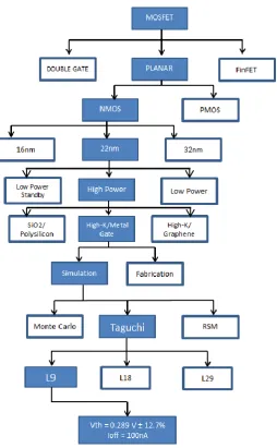
[image:24.595.202.457.103.515.2]1.4 Scope of Project
Figure 1.1: Scope of the project