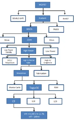
Design And Optimization Of 22 nm NMOS Device High-K/Metal Gate With Bi-Layer Of Graphene
Full text
Figure
Related documents
When the UPON option is omitted, the system logical output device (SYSOUT) is assumed. The sum of the operands may not exceed the maximum logical record length
Amniotic fluid embolism an Australian New Zealand population based study RESEARCH ARTICLE Open Access Amniotic fluid embolism an Australian New Zealand population based study
5 Amounts of glucose, flavanols and polyphenols in four kinds of wood: degraded part, apparently non-degraded sapwood, outer heartwood and inner heartwood including pith, from
“PENEGAKAN HUKUM TERHADAP TINDAK PIDANA KORUPSI PENGADAAN BARANG DAN JASA DI INDONESIA (Penerapan Konsep Hukum Progresif)” sebagai salah satu syarat untuk
Its subject areas include the analysis of space, time, offender, victim, and modus operandi for individual high-profile crimes, repeat incidents, and crime
application as compared to nonlinear controller [16-18]. In order to mitigate this, in [19] design of a linear current controller and voltage controller on the basis of gain
It can be seen that the computational complexity of the new method is much lower than that of Radon-ambiguity transform when the number of the searching angles M is far less than
