UNIVERSITI TEKNIKAL MALAYSIA MELAKA
SINGLE-PHASE CASCADED H-BRIDGE MULTILEVEL
INVERTER
This report submitted in accordance with requirement of the Universiti Teknikal Malaysia Melaka (UTeM) for the Bachelor Degree in Electrical Engineering
Technology (Industrial Power) (Hons)
by
SAIFULLAH AIZZAT BIN ABDULLAH B071110189
900419145027
ii
DECLARATION
I hereby, declared this report entitled “Single-Phase Cascaded H-Bridge Multilevel Inverter” is the results of my own research except as cited in references.
Signature : ……….
Name : SAIFULLAH AIZZAT BIN ABDULLAH
iii
APPROVAL
This report is submitted to the Faculty of Engineering Technology of UTeM as a partial fulfillment of the requirements for the degree of Bachelor of Electrical Engineering Technology (Industrial Power) with Honours. The member of the supervisory committee is as follow:
………
iv
ABSTRAK
v
ABSTRACT
vi
DEDICATION
vii
ACKNOWLEDGEMENT
viii
TABLE OF CONTENT
DECLARATION ii
APPROVAL iii
ABSTRAK iv
ABSTRACT v
DEDICATION vi
ACKNOWLEDGEMENT vii
TABLE OF CONTENT viii
LIST OF FIGURES xi
LIST OF TABLE xiii
LIST OF ABBREVIATIONS xiv
CHAPTER 1 : INTRODUCTION 1
1.1 Introduction 1
1.2 Background 2
1.3 Problem Statement 2
1.4 Objectives 3
1.5 Scope of work 3
ix
CHAPTER 2 : LITERATURE REVIEW 5
2.1 Introduction 5
2.2 Multilevel Inverter 5
2.3 AC and DC Differences 7
2.4 Cascaded H-bridge Multilevel Inverter 7
2.5 Capacitor Clamped Multilevel Inverter 9
2.6 Diode Clamped Multilevel Inverter 10
2.7 Switching Devices 11
2.8 Pulse Width Modulation (PWM) 13
2.9 Total Harmonic Distortion (THD) 14
2.10 Related Previous Works 15
CHAPTER 3 : METHODOLOGY 18
3.1 Introduction 18
3.2 Flowchart 19
3.3 Project Gantt Chart 21
3.4 Simulation Approach 23
3.4.1 MATLAB/SIMULINK 23
3.4.2 Proteus 25
3.4.3 Code Composer Studio (CCS) 26
3.5 Hardware Implementation 27
3.5.1 Etching Process 27
x
3.5.3 Driver 32
3.5.4 Checking Connection 32
3.6 Bill of Material 33
3.7 Summary 33
CHAPTER 4 : RESULT AND DISCUSSION 34 4.1 Introduction 34
4.2 Simulation Result 34
4.2.1 MATLAB/SIMULINK 35
4.2.2 THD Comparison 37
4.2.3 Code Composer Studio 37
4.3 Hardware Development Results 38 4.4 Discussion Result 42
CHAPTER 5 : CONCLUSION 43 5.1 Conclusion 43
5.2 Summary of Project 44
5.3 Problems Faced During Project 44
5.4 Future Work 45
5.5 Commercialization 45
APPENDICES 46
xi
LIST OF FIGURES
2.1 Output for 5-level multilevel inverter 6
2.2 DC AC waveform 7
2.3 Cascaded H-bridge Multilevel Inverter (Tahri et al. n.d.) 8
2.4 Capacitor Clamped Multilevel Inverter (Maheshkumar et al. 2013) 9
2.5 Diode Clamped Multilevel Inverter (Vol- & Engineering 2014) 10
2.6 a) MOSFET b) IGBT c) Diode 11
2.7 Comparison of 500V IGBT and MOSFET 12
2.8 Type of MOSFET 13
2.9 PWM 13
2.10 5-level PWM (Nurul 2012) 16
2.11 7-level PWM (Nurul 2012) 16
2.12 5-level Output (Nurul 2012) 17
2.13 7-level Output (Nurul 2012) 17
3.1 Flowchart of the Project 19
3.2 5-level cascaded H-bridge MLI 23
3.3 9-level cascaded H-bridge MLI 24
3.4 Proteus connection for 5-level 25
3.5 Connection of PCB 25
3.6 3D PCB connection 26
3.7 CCS microcontroller 26
xii
3.9 UV curing process 28
3.10 PCB Developer process 28
3.11 Cleaning process 29
3.12 Photoresist Stripper 29
3.13 Drilling Process 30
3.14 PCB etching completed 30
3.15 MOSFET soldering process 31
3.16 Complete solder circuit 31
3.17 Complete solder circuit (component) 31
3.18 Driver MOSFET 32
4.1 PWM output 35
4.2 5-level Output with PWM 35
4.3 5-level output 36
4.4 9-level output 36
4.5 CCS configuration 37
4.6 MOSFET 38
4.7 MOSFET testing 38
4.8 MOSFET output waveform 39
4.9 MOSFET driver 39
4.10 Output waveform for driver 40
4.11 5-level Cascaded H-bridge with driver 40
4.12 Input source for MOSFET 41
4.13 Input source for Driver 41
xiii
LIST OF TABLE
2.1 Comparison between Topology for THD and Component 14
2.2 5-level Switching Operations 15
2.3 7-level Switching Operation 15
2.4 Comparison between 5-level and 7-level 17
3.1 Project Gantt Chart 22
xiv
LIST OF ABBREVIATIONS
IGBT – Insulated Gated Bipolar Transistor
THD – Total Harmonic Distortion
MOSFET – Metal Oxide Semiconductor Field Effect Transistor
PWM – Pulse Width Modulation
AC – Alternating Current
DC – Direct Current
MLI – Multilevel Inverter
CHB - Cascaded H-Bridge
CCS – Code Composer Studio
1
CHAPTER 1 INTRODUCTION
1.1 Introduction
The electrical charges that are caused by physical phenomenon are called electricity and these charges produces electromagnetic fields where by it acts on another charges. The study of electricity and magnetism was first brought upon our knowledge in the year 1600 by a scientist named William Gilbert. Later, an extensive researched done Benjamin Franklin in the year 1752 through the act flying a kite during a stormy and lightning day. The lightning strike the kite and it was then discovered that lightning produces electrical charges that made up of positive and negative charge.
2
1.2 Background
This project is done to study a single phase cascaded H-Bridge multilevel inverter for 5-level output. Multilevel inverter is the source of high power, often used in industrial applications and can use either sine waves or modified sine waves. The project involves inverter consists of four H-bridge inverters that are cascaded in arrangement. For a 5-level cascaded H-bridge multilevel inverter, 8 switching devices are needed. For this project pulse width modulation (PWM) will be used as a control method. MOSFET is used as switches because of low power consumption and dissipation. The main objective is to study the single-phase cascaded multilevel inverter for 5-level.
1.3 Problem Statement
3
1.4 Objectives
Based on the problem statement above, this study is motivated by the following objectives which are:
i. To study a single phase cascaded H-bride multilevel inverter.
ii. To simulate a proposed topology using MATLAB/Simulink
iii. To implement a hardware for a proposed topology
1.5 Scope of work
A project will cover the scope of implementing hardware on circuit that utilize cascaded H bridge multilevel inverter to convert direct current to alternating current. This project can be divided into several stages or steps. Firstly, this study involve the understanding of various type of inverter and multilevel inverter focusing on the cascaded H bridge multilevel inverter. Besides, before implementing the proposed topology, it is important to study about switching especially the MOSFET as switches. Then, pulse width modulation (PWM) control method to produce the desired output that is five level output. Secondly, the MOSFET and PWM simulation and coding control are done using MATLAB. Lastly, the implementation of hardware are been tested.
4
1.6 Report outline
This documented thesis consist of five chapters. The first chapter of this thesis is Introduction which covers the project background, problem statements and the objectives of this project. The scope of study and report outline are also included in this chapter.
The second chapter of this thesis is Literature Review which focuses on reviewing previous researches or works that relates to the scope of this study. This chapter review on the implementation of various inverter and multilevel inverter for example a cascaded H-bridge multilevel inverter, a capacitor clamped multilevel inverter and a diode clamped multilevel inverter. Besides that, this chapter reviews on different type of switching devices which are insulated gated bipolar transistor (IGBT) and metal oxide semiconductor field effect transistor (MOSFET).
The third chapter of this thesis is the Research Methodology elaborates in detail of the procedures and steps taken in conducting the experiment of this project. Design and simulation software which are used to complete this project also explained in this chapter.
The fourth chapter of this thesis is Result and Discussion. This chapter discusses about the result from the five level output of the single phase cascaded H bridge multilevel inverter. The structure and setup of the cascaded H bridge multilevel inverter that uses 8 switches will also be discussed.
5
CHAPTER 2
LITERATURE REVIEW
2.1 Introduction
This chapter will be discussing about the overview of multilevel inverter including 2-level inverter. Mainly about cascaded H-bridge multilevel inverter, capacitor clamped multilevel inverter, diode clamped multilevel inverter and their switching devices and related result by other research will also be discussed.
2.2 Multilevel Inverter
6 this type inverter can be used in high power and high voltage application because of its efficiency, low in total harmonic distortion (THD) and low in switching losses (Orfanoudakis et al. 2010). Multilevel inverter means that the inverter have more than two level such as 3 level, 5 level, 9 level and 11 level compare to normal inverter that only have two level. There are many different topologies to build a multilevel inverter. The one that have been proposed for this project is a cascaded H-bridge multilevel inverter (Tahri et al. n.d.). Others topology is a capacitor clamped multilevel inverter also known as a flying capacitor multilevel inverter and a diode clamped multilevel inverter (Vol- & Engineering 2014). The three topologies are widely used in high power application because of low switching losses and low in THD (Multilevel n.d.). Study by previous works show that cascaded H-bridge multilevel inverter is the best option for medium voltage and high power application due to the lowest THD among others topology (Inverter & Booma 2011). Figure 2.1 shows an output for 5-level multilevel inverter.
7
2.3 AC and DC Differences
The device use to convert direct current (DC) to alternating current (AC) is inverter. To know the concept of inverter firstly the understanding of AC/DC is important. Current that move in one direction is called direct current (DC) while current that can change direction in positive cycle or negative cycle is called alternating current (AC). This project is to build an electronic device that can convert DC to AC for high voltage and high power application. Figure 2.2 shows a DC AC waveform.
2.4 Cascaded H-bridge Multilevel Inverter
[image:21.595.219.452.324.436.2]Cascaded H-bridge multilevel inverter is the simplest multilevel inverter compare to other multilevel inverter (Tahri et al. n.d.). This multilevel inverter contain of H-bridges connected in series that has a separate DC source that can produce a desired output voltage. The Dc source can be from solar cells, wind turbine or battery. This make cascaded H-bridge popular for renewable energy because of separate DC sources. (Tahri et al. n.d.) Figure 2.3 show 5 level cascaded H-bridge multilevel inverter circuit.
8 Figure 2.3: Cascaded H-bridge Multilevel Inverter (Tahri et al. n.d.)
Advantages:
Lowest in component used
Lowest in total harmonic distortion (THD) (Lokeshwari 2014) Simple circuit
Voltage stress is reduce Transformer less
Not expensive compare to other multilevel inverter.
Disadvantages:
Separated DC sources.
9
2.5 Capacitor Clamped Multilevel Inverter
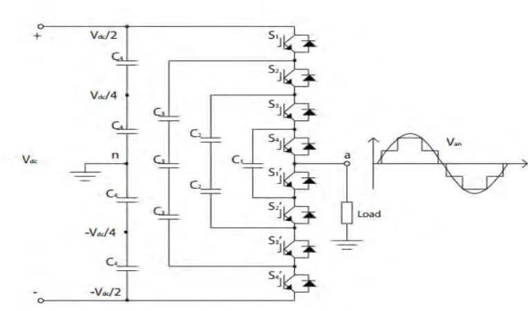
[image:23.595.155.537.240.465.2]Flying capacitor multilevel inverter also known as capacitor clamped multilevel inverter this is because of its independent capacitor clamped the voltage to another capacitor voltage level (Maheshkumar et al. 2013). If the output level needed is high, the amount of capacitor used also increase. Figure 2.4 show the capacitor clamped multilevel inverter circuit.
Figure 2.4: Capacitor Clamped Multilevel Inverter (Maheshkumar et al. 2013)
Advantages:
real and reactive power flow can be control get the desired voltage value by using capacitor.
Disadvantages:
complicated to control compare to other topology
10
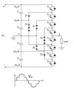
2.6 Diode Clamped Multilevel Inverter
[image:24.595.176.486.244.623.2]Diode clamped multilevel inverter is using diode as the main component. The use of the diode is to clamp the dc bus voltage for level output voltage. The main function of diodes is to limit the power devices voltage stress. Figure 2.5 show the diode clamped multilevel inverter circuit.