Rochester Institute of Technology
RIT Scholar Works
Theses Thesis/Dissertation Collections
5-2016
Effects of Solder Paste Volume on PCBA Assembly
Yield and Reliability
Sai Srinivas Sriperumbudur [email protected]
Follow this and additional works at:http://scholarworks.rit.edu/theses
This Thesis is brought to you for free and open access by the Thesis/Dissertation Collections at RIT Scholar Works. It has been accepted for inclusion in Theses by an authorized administrator of RIT Scholar Works. For more information, please [email protected].
Recommended Citation
i
EFFECTS OF SOLDER PASTE VOLUME ON PCBA ASSEMBLY
YIELD AND RELIABILITY
By
SAI SRINIVAS SRIPERUMBUDUR
A Thesis Submitted in Partial Fulfillment of the Requirements for the Degree of Master of Science in Manufacturing and Mechanical Systems Integrations
Supervised by
Dr. Martin Anselm
Department of Manufacturing and Mechanical Engineering Technology College of Applied Science and Technology
Rochester Institute of Technology Rochester, NY
May, 2016
Approved By:
_____________________________________________ ___________ ___
Dr. Martin Anselm
Primary Advisor – R.I.T. Dept. of Manufacturing and Mechanical Engineering Technology
_ __ ___________________________________ _________ _____
Dr. S. Manian Ram Kumar
Secondary Advisor – R.I.T. Dept. of Manufacturing and Mechanical Engineering Technology
_____________________________________________ ______________
Dr. Duane Beck
ii
Acknowledgements
I am sincerely grateful to Dr. Ram Kumar and Dr. Martin Anselm for their
constant guidance and support during the entire course of my study. Their valuable inputs
and critiques have enabled me to develop a strong researching technique that has been of
immense help in the professional aspects of my work. I would like to thank Dr. Duane
Beck for being part of my committee and providing their valuable inputs on my research
work. I am also grateful to all my professors who taught the courses that I have taken
during my master’s degree.
I would like to thank my mentor at Universal Instruments, Michael Meilunas for
his constant support and continuous encouragement for my research work as well as the
other project related activities. I would also like to thank Dr. Jim Wilcox and the whole
team of Universal Instruments Advanced Processing Lab for their invaluable funding and
intellectual support during this research. I will be personally indebted to them for their
guidance and support that enabled me to rise to the expectations of the professional work
iii
Abstract
Solder paste printing is the most common method for attaching surface mount devices to
printed circuit boards and it has been reported that a majority of all assembly defects
occur during the stencil printing process. It is also recognized that the solder paste
printing process is wholly responsible for the solder joint formation of leadless package
technologies such as Land Grid Array (LGA) and Quad-Flat No-Lead (QFN) components
and therefore is a determining factor in the long-term reliability of said devices. The goal
of this experiment is to determine the acceptable lower limit for solder paste volume
deposit tolerances during stencil printing process to ensure both good assembly yield and
reliability expectations. Stencils with modified aperture dimensions at particular locations
for LGA and QFN package footprints were designed in order to vary the solder paste
volume deposited during the stencil printing process. Solder paste volumes were
measured using Solder Paste Inspection (SPI) system. Low volume solder paste deposits
were generated using the modified stencil designs to evaluate assemble yield.
Accelerated Thermal Cycling (ATC) was used to determine the reliability of the solder
joints. For the LGAs, solder joints formed with higher paste volume survived longer in
ATC compared to lower volume joints. Low solder paste volume deposits did not affect
BGA devices in ATC. Transfer efficiency numbers for both good assembly yield and
good reliability are reported for LGA, QFN and BGA devices. This research provides
valuable data because, very little data is available on solder paste volume tolerance limits
in terms of assembly yield and reliability. Manufacturers often use ±50% of stencil
aperture volume with no evidence of its effectiveness in determining yield and reliability
iv
Table of Contents
Acknowledgements... ii
Abstract ... iii
List of Tables ... vi
List of Figures ... vii
List of Abbreviations ... xi
Chapter 1: Introduction to Research ... 1
1.1 Introduction ... 1
1.2 Problem Statement ... 3
1.3 Research Objective ... 4
1.4 Research Methodology ... 4
Chapter 2: Literature Review ... 5
2.1 Introduction ... 5
2.2 Solder Paste Printing ... 6
2.2.1 Factors affecting solder paste printing ... 9
2.2.2 Evaluation of the solder paste printing process... 14
2.2.3 Solder paste rheology ... 18
2.2.4 Optimization of stencil printing parameters ... 19
2.3 SMT defects due to poor solder paste printing ... 20
2.3.1 Insufficient solder ... 21
2.4 Solder Paste Inspection ... 22
2.4.1 Need for Solder Paste Inspection ... 22
2.4.2 Determining Solder Paste Inspection (SPI) variance ... 24
2.4.3 Functioning of Solder Paste Inspection machine ... 26
2.4.4 Importance of true height measurement ... 30
Chapter 3: Research Methodology ... 32
3.1 Introduction ... 32
3.2 Research Overview ... 32
3.3 Test Vehicle ... 36
3.4 Package Types ... 38
v
3.4.2 Land Grid Array (LGA) 97 ... 39
3.4.3 Quad Flat No Lead (QFN) 100 ... 40
3.4.4 Quad Flat No Lead (QFN) 156 ... 41
3.4.5 BGA 144 ... 42
3.4.6 BGA 360 ... 42
3.5 Stencil Designs... 43
3.6 Equipment and process setting ... 48
3.6.1 Stencil Printer ... 48
3.6.2 Solder Paste Inspection System ... 49
3.6.3 Component Placement Machine ... 50
3.6.4 Reflow Oven ... 51
3.6.5 X-Ray Inspection... 53
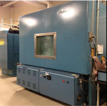
3.6.6 Thermal Chamber ... 54
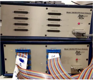
3.6.7 Event Detector ... 55
Chapter 4: Results and Discussions ... 56
4.1 Assembly Results... 56
4.1.1 LGA 208 ... 56
4.1.2 LGA 97 ... 59
4.1.3 QFN 100 ... 62
4.1.4 QFN 156 ... 66
4.1.5 BGA 144... 67
4.1.6 BGA 360... 70
4.2 Reliability Results ... 73
4.2.1 LGA 208 on Cu-OSP ... 73
4.2.2 LGA 208 on ENIG ... 77
4.2.3 LGA 97 on Cu-OSP ... 78
4.2.4 QFN 100 on Cu-OSP ... 80
4.2.5 QFN 156 on Cu-OSP ... 82
4.2.6 BGA 144 on Cu-OSP: ... 84
4.2.7 BGA 360 on Cu-OSP... 86
4.3 Conclusion ... 87
vi
List of Tables
Table 1 SPI solder volume% information for X board (chen, 2011) ... 25
Table 2 SPI solder volume% information for Y board (Chen, 2011)... 25
Table 3 SPI solder volume % information for Z board (Chen, 2011) ... 25
Table 4 Summary of stencil designs ... 44
Table 5 Transfer efficiencies ranges tested in ATC. ... 73
vii
List of Figures
Figure 1 Through Hole Technology... 1
Figure 2 Surface Mount Technology ... 2
Figure 3 Break down of SMT defect (Biemans,2011) ... 3
Figure 4 Stencil Printing Process (Pan,1999) ... 8
Figure 5 Aperture Emptying Process (Durairaj, 2001) ... 8
Figure 6 Dimensions of stencil aperture (Burr, 1998) ... 10
Figure 7 Solder paste printing variables (Amalu, 2011) ... 12
Figure 8 A hierarchical view of influence variables of stencil printing (Yang, 2005) ... 13
Figure 9 Perpendicular and Parallel Apertures (Pan, 1999) ... 17
Figure 10 Constituents of solder flux (Amalu, 2011) ... 18
Figure 11 Effect of stencil thickness on print defects (Lee, 2001) ... 21
Figure 12 Rework cost and 10X rule (Riddle, 2007) ... 23
Figure 13 Contrast base, gray scale image Figure 14 Textured base image (Mohanty, 2008) ... 27
Figure 15 2D image of solder deposits (Mohanty, 2008) Figure 16 Segmented 2D image of solder deposits ... 27
Figure 17 Height calculation using Moiré topography (Biemans, 2011) ... 29
Figure 18 Solder Paste Height Value under normal condition and after filtering Source (Kulkarni, 2014) ... 31
Figure 19 Reflow Profile ... 34
Figure 20 Thermal Cycling profile -400C to 1250C ... 36
Figure 21 Test Vehicle bare board Cu-OSP surface finish ... 37
Figure 22 Test Vehicle Assembled ... 38
Figure 23.LGA 208 ENIG, Cu-OSP surface finish coupons and component bottom side ... 38
Figure 24 Cu-OSP surface finish coupons and component bottom side ... 39
Figure 25 Cu-OSP surface finish coupons and component bottom side ... 40
Figure 26.QFN156 Cu-OSP surface finish coupon and component bottom side ... 41
Figure 27 BGA 144 Cu-OSP surface finish coupon and component bottom side ... 42
Figure 28 BGA 360 Cu-OSP surface finish coupon and component bottom side ... 42
Figure 29 LGA 208 stencil aperture layout. Green indicates standard stencil aperture positions, red indicates undersized aperture positions. ... 45
Figure 30 LGA 97 stencil aperture layout. Green indicates standard stencil aperture positions, red indicates undersized aperture positions. ... 45
Figure 31 LGA 208 stencil aperture layout. Green indicates standard stencil aperture positions, red indicates oversized aperture positions.... 46
viii
Figure 33 QFN 156 stencil aperture layout. Green indicates standard stencil aperture positions,
red indicates undersized aperture positions. ... 47
Figure 34 BGA 144 stencil aperture layout. Green indicates standard stencil aperture positions, red indicates undersized aperture positions. ... 47
Figure 35 BGA 360 stencil aperture layout. Green indicates standard stencil aperture positions, red indicates undersized aperture positions. ... 48
Figure 36 Stencil Printer ... 48
Figure 37 Solder Inspection System... 50
Figure 38 Component Placement Machine ... 50
Figure 39 Reflow Oven ... 51
Figure 40 Reflow Oven User Interface ... 52
Figure 41 X-Ray Inspection System ... 53
Figure 42 Thermal Chamber ... 54
Figure 43 Event Detector ... 55
Figure 44 LGA 208 paste volume distribution for standard aperture ... 56
Figure 45 Comparison of Standard Aperture (SA) paste deposit volumes and Undersized Apertures (UA1, UA2, UA3) paste deposit volumes used to assemble LGA 208 on Cu-OSP motherboards. ... 57
Figure 46 X-ray image of LGA 208 on Cu-OSP with a non-functional solder joint with 45% TE (317 mil3). ... 58
Figure 47 Comparison of Standard Aperture (SA) paste deposit volumes and Undersized Apertures (UA1, UA2, UA3) paste deposit volumes used to assemble LGA 208 on ENIG motherboards. ... 58
Figure 48 X-ray image of LGA 208 on ENIG with a functional solder joint with 40% TE (309 mil3). ... 59
Figure 49 LGA 97 paste volume distribution for standard aperture. ... 60
Figure 50 Comparison of Standard Aperture (SA) paste deposit volumes and Undersized Apertures (UA1, UA2, UA3) paste deposit volumes used to assemble LGA 97 on Cu-OSP motherboards. Joints formed with the equivalent of 37% TE or less was electrically unacceptable. ... 61
Figure 51 X-ray image of LGA 97 on Cu-OSP with a non-functional solder joint with ~37% TE (156 mil3). ... 62
Figure 52 QFN 100 paste volume distribution for standard aperture design. Bimodal distribution is apparent. ... 63
Figure 53 Comparison of Standard Aperture (SA) and Undersized Aperture (UA1,UA2,UA3) paste deposit volumes used to assemble QFN 100 to Cu-OSP motherboards. Deposit sizes greater than 135mil3 formed functional solder joints. ... 64
Figure 54 X-ray image of QNF 100 on Cu-OSP with a functional solder joint with 15% TE (135 mil3 ). ... 65
Figure 55 QFN 156 paste volume distribution for standard aperture. ... 66
ix
Figure 57 BGA 144 paste volume distribution for standard aperture. ... 68
Figure 58 Comparison of Standard Aperture (SA) paste deposit volumes and Undersized Apertures (UA1,UA2) paste deposit volumes used to assemble BGA 144 to Cu-OSP
motherboards. ... 69
Figure 59 X-ray image of BGA 144 on Cu-OSP with a functional solder joint with ~30% TE (215 mil3). ... 70
Figure 60 BGA 360 paste volume distribution for standard aperture. ... 71
Figure 61 Comparison of Standard Aperture (SA) paste deposit volumes and Undersized Apertures (UA1, UA2) paste deposit volumes used to assemble BGA 360 to Cu-OSP
motherboards. ... 72
Figure 62 X-ray image of BGA 360 on Cu-OSP with a functional solder joint when no paste was printed on the pad. ... 72
Figure 63 Weibull plot comparing solder joint reliability of control LGA 208 samples with Target T.E 85% and Target T.E 70% LGA 208 samples on Cu-OSP surface finish. ... 74
Figure 64 a. LGA 208 control sample corner joint failure @ 428 cycles, b. LGA 208 85% sample corner joint failure @ 341 cycles, c. LGA 208 75% sample corner joint failure @ 335 cycles. ... 75
Figure 65 Cycles to Failure Vs. Volume for LGA 208 on Cu-OSP PCB. ... 76
Figure 66 Weibull plot based on Transfer Efficiency of the failed joint of LGA 208 on Cu-OSP motherboards. ... 77
Figure 67 a. LGA 208 120% sample corner joint failure @578 Cycles, b. LGA 208 Control sample corner joint failure @387 Cycles, c. LGA 208 85% sample corner joint failure @353 Cycles. ... 77
Figure 68 Weibull plot comparing solder joint reliability of control LGA 208 samples with Target T.E 120% and Target T.E 85% LGA 208 samples on ENIG surface finish. ... 78
Figure 69 Weibull plot comparing solder joint reliability of control LGA 97 samples with Target T.E 85% and Target T.E 70% LGA 97 samples on Cu-OSP surface finish. ... 79
Figure 70 Weibull plot comparing solder joint reliability of control QFN100 samples to Target TE 50% and Target TE 40% QFN100 samples. ... 81
Figure 71 a. QFN 100 control sample corner joint failure @976 Cycles, b. QFN 100 target TE 50% sample corner joint failure @919 Cycles, c. QFN 100 target TE 40% sample corner joint failure @691 Cycles.... 82
Figure 72 Weibull plot comparing solder joint reliability of control QFN 156 samples with Target T.E 50% and Target T.E 40% QNF 156 samples. ... 83
Figure 73 a. QFN 156 control sample corner joint failure @362 Cycles, b. QFN 156 target T.E 50% sample corner joint failure @393 Cycles, c. QFN 156 target T.E 40% sample corner joint failure @386 Cycles.... 84
Figure 74 Weibull plot comparing solder joint reliability of control BGA144 samples with Target T.E 50% and Target T.E 40% BGA 144 samples. ... 84
Figure 75 . a) BGA 144 control sample corner joint failure @972 cycles, b) BGA 144 target T.E 50% sample corner joint failure @783 Cycles , c) BGA 144 target T.E 40% sample corner joint failure @915 Cycles.... 85
x
Figure 77 a. Corner joint failure of standard joint of target 40% TE sample; b. Undersized functional joint of the sample in adjacent figure. ... 86
Figure 78 Weibull analysis of LGA 208 on Cu-OSP ... 88
xi
List of Abbreviations
SMT Surface Mount Technology
SMD Surface Mount Device
THT Through Hole Technology
SPI Solder Paste Inspection
PCB Printed Circuit Board
ATC Accelerated Thermal Cycling
LGA Land Grid Array
BGA Ball Grid Array
QFN Quad-Flat-No-Leads
TAL Time Above Liquidus
TE Transfer Efficiency
BTC Bottom Terminated Components
CTE Coefficient of Thermal Expansion
SA Standard Aperture
1
Chapter 1: Introduction to Research
1.1 Introduction
Integrated circuits are packed in different kinds of packages to protect them from heat,
humidity, electrical discharges and other environmental factors which may affects the
functionally of the integrated circuit. These packages provide electrical connections
between various components and the PCB and help to make the assembly of the
integrated circuit on to the printed circuit boards (PCB’s) an easy process. There are two
major assembly techniques used to assemble these packages on to the PCB,
Through-Hole Technology (THT) and Surface Mount Technology (SMT). Through-hole
technology refers to the mounting scheme used for electronic components that involves
the use of leads on the components that are inserted into holes drilled in the PCB and
soldered to pads on the opposite side either by manual assembly (hand placement) or by
the use of automated insertion mount machines. Figure 1 shows a graphic of a PCB
assembled with THT.
Figure 1 Through Hole Technology
SMT is a method of attaching components on to the PCB surface directly with solder
2
placement machine and a reflow oven. Electronic devices designed for this technology
are called Surface-Mount Devices (SMD). SMT has almost replaced the traditional
through-hole technology (THT) in the current industry. Both technologies can be used on
the same boards according to the product requirement. Figure 2 represents a graphic of a
PCB assembled using SMT.
Figure 2 Surface Mount Technology
Some of the package types used for SMT either have solder balls attached to the bottom
of the package like Ball Grid Arrays (BGA’s) or have flat surface without any leads like
Land Grid Arrays (LGA’s) and Quad Flat No Leads (QFN’s) also known as Bottom
Terminated Devices (BTCs).
Majority of defects in SMT process can be related to stencil printing process (Biemans
3
Figure 3 Break down of SMT defect (Biemans,2011)
A reliable solder joint is dependent on the solder paste volume deposition on the PCB
during stencil printing process. Different package types have different solder paste
volume requirements. To eliminate the defects during stencil printing process solder paste
inspection machines (SPI) are being used to screen the PCB’s after stencil printing
process. The SPI machine scans the PCB’s with a shadow moiré technique and high
resolution cameras to calculate the solder paste deposit volume. This can then be used to
determine if the deposit is acceptable based on the tolerances set by the operator.
1.2 Problem Statement
The SPI tolerance limits are determined subjectively. Review of literature also indicates
that there is little research done on the determination of SPI tolerance limits. Many
manufacturers set the allowable paste volume tolerance to +/-50% of the stencil aperture
volume with little or no evidence of its effectiveness in determining yield and reliability
4
determination of SPI tolerance limits should be based on feedback from post-reflow
inspection (Huang C 2011) and reliability testing. SPI machine set up with incorrect
tolerance limits would become ineffective in catching print related defects. So the
problem of subjective SPI tolerance limits is addressed in this report, by determining SPI
tolerance limits based on assembly yield results and reliability results.
1.3 Research Objective
The goal of this research is to determine the SPI tolerances limits for different package
types to achieve good yield and reliability. Different stencil designs with different
aperture sizes configurations are used to vary the solder paste volume. The SPI tolerance
limits are determined from assembly yield data and reliability data generated from this
experiment.
1.4 Research Methodology
This thesis work is performed in two stages. In stage one, several boards were printed and
paste volume data was collected and analyzed. Based on the print volume data several
stencil designs were designed. All the stencils used were stainless steel laser cut stencils
from DEK. At the end of stage one SPI tolerance limits for good assembly yield were
determined. In stage two all the boards assembled with SPI tolerance limits from stage
one were subjected to Accelerated Thermal Cycling (ATC) and reliability of those
packages were determined in terms of paste volume. Suggestions for SPI tolerance limits
were made to achieve high assembly yield and good reliably. A detailed explanation of
5
Chapter 2: Literature Review
2.1 Introduction
SMT is the process of soldering electronic components onto the conductive pads of PCB.
The SMT process consists of three sub-processes: printing solder paste onto the substrate,
automatic placement of components onto their designated locations and reflow of the
substrate along with components to form a solder joint. The Literature Review shows that
52-71% of SMT defects can be attributed to the solder paste printing process (Jianbiao
Pan 1999). As the trend of product miniaturization continues to happen, the need for
assembling area array type packages with high I/O increases. The assembly of these area
array packages involves depositing very small solder paste deposits, wherein the surface
tension effects are dominant over the viscous flow of the solder paste. For this reason,
printing of solder paste through small apertures usually results in stencil clogging and
incomplete paste transfer. An in-depth understanding of how to screen the defects is
6
2.2 Solder Paste Printing
In the solder paste printing process, solder paste is deposited onto the PCBs before
placing the components with the help of a stencil printer. The advantage of doing it is to
achieve high production speed and cost reduction, stencil printing is widely adopted in
the industry for solder paste printing.
According to (Amalu 2011), controlling the exact amount of solder paste deposited on the
PCB is one of the main challenges at second level packaging. The solder paste deposited
on the solder pads varies from pad to pad within a PCB, and it also varies from one PCB
to another. This inconsistency is because of many variables involved in the stencil
printing, and the problem of not achieving consistent printing becomes worse with fine
pitch apertures. Hence, there is a need for a better understanding of solder paste printing
process (Amalu 2011). According to (Nguty 1999) the quality of solder paste printing
process is dominated by the flow of solder paste into the stencil aperture and the aperture
emptying process. The Solder paste must have the ability to deform easily into the stencil
aperture when sheared and flow out of the stencil aperture during paste release (Durairaj
2001). According to (Yang 2005) three sequential stages in stencil printing proces are
illustrated in Figure 4. In the first stage, a squeegee forces the solder paste to roll in front
of its blade for some distance before shearing off the paste in stencil apertures as the
squeegee moves over the stencil. In the second stage, the hydrodynamic pressure that is
7
in the third stage, solder paste is left on the pad of the substrate after the PCB is
mechanically separated from the stencil. As the board moves away from the stencil, the
solder paste experiences forces at the pad surface and aperture walls. As shown in Figure
5, the adhesive frictional force operating between the stencil walls and the solder paste
competes directly with the adhesive pull force between the solder paste and the PCB
bond pad. The net force determines the final release of paste from the stencil aperture
8
Figure 4 Stencil Printing Process (Pan,1999)
9
2.2.1 Factors affecting solder paste printing
A number of process parameters influence the solder paste printing process. According to
(Haslehurst.L. 1996), the process parameters can be categorized into four groups: printer,
paste, environmental and stencil. Squeegee pressure, squeegee speed, stencil separation
speed and print direction are the key processes in stencil printing. Literature Review
indicates that area ratio and aspect ratio are important factors in addressing the challenges
of solder paste printing (Durairaj 2001), showed experimentally that aspect ratio should
be higher than 1.25 and area ratio should be greater than 0.6. Paste transfer is also
directly impacted by particle size and other paste related properties.
2.2.1.1 Aspect ratio and Area ratio
Aspect ratio is defined as the ratio of aperture width (W) to the stencil thickness (T).
Aspect Ratio = 𝐴𝑝𝑒𝑟𝑡𝑢𝑟𝑒 𝑊𝑖𝑑𝑡ℎ
𝑆𝑡𝑒𝑛𝑐𝑖𝑙 𝑇ℎ𝑖𝑐𝑘𝑛𝑒𝑠𝑠 = 𝑊
𝑇 (Durairaj 2001)
Area ratio is defined as the ratio of the area of the aperture opening (L*W) to the area of
the aperture wall (2T * (L+W))
Area Ratio = 𝐴𝑟𝑒𝑎 𝑜𝑓 𝑎𝑝𝑒𝑟𝑡𝑢𝑟𝑒 𝑜𝑝𝑒𝑛𝑖𝑛𝑔
𝐴𝑟𝑒𝑎 𝑜𝑓 𝑎𝑝𝑒𝑟𝑡𝑢𝑟𝑒 𝑤𝑎𝑙𝑙 = 𝐿∗𝑊
2∗𝑇∗(𝐿+𝑊) (Durairaj 2001)
The dimensions of stencil aperture used in the calculation of Aspect ratio and Area ratio
10
11
(Amalu 2011), grouped the critical variables, that influence the solder paste deposition,
into five categories: Solder Paste, Stencil, Substrate, Printer and Environmental
parameters that are shown in Figure 7. The stencil and substrate parameters do not
change during the manufacturing process, but the remaining three of the five parameters
stated above, vary either automatically or on their own. A change in properties of the
12
13
(Yang 2005), proposed “a hierarchical view of influence variables of the stencil printing” that is shown in Figure8.
14
2.2.2 Evaluation of the solder paste printing process
(Lau 1997), evaluated the solder paste printing process and developed the five level
hierarchies for the solder paste printing process and states that such hierarchical
evaluation of the solder paste printing process is essential for improving the concerned
process. According to (Lau 1997), following are the five major factors that determine the
quality of solder joint: (i) The choice of stencil opening geometry; (ii) The matching of
the solder paste; (iii) The control of the waiting time (iv) The selection of the squeegee
material; and (v) The parameter setting of printing machine. Descriptions of the five
factors mentioned are as follows:
2.2.2.1 Choice of stencil opening geometry
Chemical etching, laser cutting, and electroforming are the three different stencil
fabrication processes that are used in the stencil manufacturing industry. The Chemical
etching process usually produces a knife edge shaped aperture opening, which affects the
release of solder paste especially when the aperture opening is less than 25µm. Therefore,
an additional process called electropolishing is employed after chemical etching, to
smoothen the knife edge shaped aperture openings. The laser cutting process yields a
stencil opening such that the bottom is slightly larger than the top, and such internal taper
on aperture walls favors the better release of solder paste from the stencil. The
electroforming process can produce a stencil with very fine and smooth aperture with
vertically tapered walls. The stencils fabricated through the electroforming process favors
15
2.2.2.2 Matching of solder paste
The quality of the solder paste printing process is greatly influenced by the composition
of solder paste and its corresponding properties. Few characteristics of the solder paste,
such as viscosity, wetting, metal composition, particle shape and size, and also the flux
activity play a significant role in the solder paste printing process (Lau, 1997).
2.2.2.3 Control of waiting time
The wait time of the solder paste after being deposited onto their designated solder pads
affects the solder joint quality. This is because after solder paste printing, the paste
slumps, spreads and absorbs moisture from the environment. The slumping effect gets
more significant for fine pitch components than when compared with normal
components. Excessive wait time can also lead to other defects such as solder balls.
Therefore, the wait time before reflow should be controlled (Lau, 1997).
2.2.2.4 Selection of squeegee material
A squeegee is used to spread the solder paste across the stencil and allow the transfer of
solder paste through the stencil onto the PCB. A harder squeegee favors better paste
transfer when compared to a softer squeegee. A soft squeegee is preferred while using a
stepped stencil. However, using a soft squeegee may cause scooped printing, due to the
spring back property of the soft squeegee. A metal squeegee, usually made from stainless
16
2.2.2.5 Settings of solder printing process
The solder paste printing process is highly affected by five print machine parameters.
Those are printing pressure, printing speed, snap off, parallelism of the squeegee, and the
squeegee angle. “Environmental conditions such as humidity and temperature also impact
the solder printing process” (Lau, 1997). The effects of the parameters mentioned above
are explained below
Low print speed may lead to inconsistent fill in of stencil apertures because the low
squeegee speed may not favor the roll of solder paste in front of the squeegee. High print
speed will cause loss of viscosity in the solder paste that may lead to slumping and
misprint. High pressure may push down the squeegee into stencil apertures and scoop out
some of the solder paste. On the other hand, if the squeegee pressure is too light, the
solder paste may not adhere to the solder pads. The distance to which the PCB is
mechanically separated at a controlled speed is known as the snap-off distance. The
squeegee angle is the angle at which the squeegee gets in contact with the stencil. The
squeegee angle affects the forces that are required to roll the solder paste in front of the
squeegee and push the solder paste into the stencil apertures. When the squeegee travel
direction is perpendicular to the longer side of the stencil aperture, then the aperture is
called a perpendicular aperture. When the squeegee travel direction is parallel to the
longer side of the stencil aperture, then the aperture is called parallel aperture. Both
perpendicular and parallel apertures are shown in Figure 9. (Jianbiao Pan 1999), showed
experimentally that a stencil with perpendicular apertures can deposit 5-6% more volume
17
18
2.2.3 Solder paste rheology
For several reasons such as low cost, a low melting point when compared to its
alternatives, good mechanical strength and comparatively good solderability,
Sn-Ag-Cu(SAC) solder alloy is considered as the most promising lead-free solder alloy (Kim
2003). As the print quality of the solder paste is directly impacted by its rheological
properties such as flow, slump resistance, and tack value, rheology of solder paste is
gaining significance (Mallik 2008), proposed that microscopic distributions of solder
powders strongly affect the rheological behavior of the solder paste. The solder paste is
considered as a non-Newtonian fluid that exhibits thixotropic behavior. Amalu, et al.
(2011), established the way the transfer efficiency of lead-free solder is affected by
“solder paste rheology and stencil aperture cavity size” (Amalu 2011). According to
(Durairaj 2001), consistent withdrawal of the solder paste is highly dependent on the
paste rheology at minuscule aperture sizes. This is because the surface tension dominates
viscous flow at smaller aperture sizes and, therefore, impacts the paste transfer efficiency.
The constituents of the solder flux are shown below, in Figure 10.
19
2.2.4 Optimization of stencil printing parameters
Stencil print parameters play a key role in improving the SMT yield. This section lists the
important print parameters and the research that have been done in the optimization of
those key print parameters.
(Sekharan 2006), conducted a half factorial DOE by considering five factors at two levels
and obtained optimal settings for a solder paste printing process. squeegee pressure,
squeegee speed, snap off, separation speed and stencil wipe frequency were the five
different factors that were considered for performing the DOE. The height of the solder
paste deposition was considered as a response variable. The interactions of the snap off
and the separation speed, the print speed and the squeegee pressure, and the separation
speed and the stencil wipe frequency were identified as significant interactions that
influenced the solder paste height deposition. The results of the DOE indicated that
among the two levels chosen for each factor, a high squeegee pressure, high printing
speed, low snapoff , low separation speed were part of optimal print parameters. The
authors have also shown a 20% percent improvement in response variable by performing
a validation run with the optimal print parameters.
Pan, et al. (2004), identified the critical variables that influence the height, area, and
volume of the solder paste deposition. The authors used ANOVA to examine the
influence of aperture size and shape, thickness of the stencil, surface finish of the board,
solder paste type and print speed on the solder paste deposition. Their analysis has shown
that thickness of the stencil and size of the aperture are the two most critical variables that
20
(Liu 2006), employed a Taguchi DOE approach to investigate the effect of the stencil
thickness, the squeegee pressure, the PCB separation speed, and the squeegee speed on
the stencil printing process. The transfer efficiency of solder paste volume was
considered as a response variable in the experiment. Out of the four factors studied,
stencil thickness had an obvious effect on the volume transfer efficiency. The PCB
separation speed and the squeegee printing speed had a minor effect, and squeegee
pressure had no significant effect on the response variable. Quicker separation of the PCB
contributed towards a higher transfer efficiency.
2.3 SMT defects due to poor solder paste printing
The usage of miniature components continues to increase as the demand for small
handheld devices is increasing day-by-day. The manufacturing defects that occur during
the assembly of the components can affect the service life of the small handheld devices.
Hence, there is a requirement to understand these defects and stop/control these defects at
the assembly level. According to (Ladani 2008) the most frequent defects such as smear,
insufficient solder, component shift, tombstoning, and solder bridging, are directly related
to solder paste printing and solder reflow process. The following section of this report
includes a brief description of several defects that are related to poor solder paste
21
2.3.1 Insufficient solder
Insufficient solder is a common problem at the stencil printing stage. Here the aperture
clogging does not allow complete transfer of solder paste and, as a result, the deposited
solder volume is less than target solder volume. Insufficiency is caused by a few factors
such as (1) Inadequate paste rheology (2) stencil thickness (3) aperture orientation (4)
pitch dimension (5) improper aperture design (6) insufficient squeegee pressure (7)
powder size (8) poor aperture quality. According to (Lee 2001), as the pitch decreases
below 30mils, the print defect rate increases very rapidly. At a pitch below 30 mils,
insufficiency becomes a dominant defect because clogging of the stencil aperture
increases with decreasing aperture size (Lee 2001) as shown in Figure 11.
22
2.4 Solder Paste Inspection
2.4.1 Need for Solder Paste Inspection
The solder paste printing process is a crucial assembly process in SMT that determines
the quality of the solder joints. According to (Burr, 1997) the solder paste printing
process is considered a “black art” because there are 39 variables involved in the solder
paste printing process and the relationship between those 39 variables is not completely
understood. The volume of the solder paste deposited onto the PCB is considered to be a
good predictor of solder joint reliability and for this reason; an ideal printing process is
aimed at achieving consistent volume on a repeatable basis (Biemans 2011).
The boards rejected due to defects would either be reworked or scrapped. Rework is a
non-value adding process, and it requires excessive cost and resources. If not properly
controlled, reworked solder joints can be less reliable and susceptible to fail. Reworked
solder joints are less reliable and are vulnerable to fail at customer site which can lead to
expensive warranty repairs. Scrapping a board incurs additional cost to the manufacturer
and also affects their product delivery timelines. The excess cost of rework and constant
market pressure to reduce cycle time has driven the manufacturer to look for ways to
reduce or eliminate defects upstream in the process (Burr, 1997).
Value added to the board increases as the board moves from one stage to another.
Because of this reason, it is desirable to catch and prevent defects at an early stage.
Washing a misprinted board consumes much less cost and resources than the resources
23
the 10X rule, which states that the rework cost at each stage will be ten times greater than
that in the previous stage. For instance if correcting a misprint of solder paste is
calculated to be $0.50, correcting the failure after reflow would cost $5.00 and correcting
the same failure after the board is integrated into the system would cost $50.00. If
somehow the defect escapes from all the inspection stages and the board fails at the
customer site, the cost to recall the product and correct it could be as high as $500.00 or
even more (Riddle 2007). The 10X rule could easily justify the cost and resources
invested in setting up a SPI machine and implementing an in-line solder paste inspection.
The 10X rule explained in Figure 12. Many electronics manufacturing services providers
have a market requirement to perform 100% solder paste inspection. “These factors
combined with the ongoing need for continuous process improvement drives the need for
solder paste inspection” (Gunn 2001).
24
Inspection of the solder paste after printing is a potential way to eliminate or reduce most
of the defects. Numerous publications are available online which reiterate the importance
of an in-line SPI machine. According to (Johnson 2003), if a SPI machine is useful for
stopping at least a few customer site board failures, the investment made on the SPI
machine would be recovered within a short period. According to Daniels (1996), EMS
providers believe that their profit margins can be increased by increasing the process
quality but not by quoting higher prices or by lowering quality standards. The profit that
manufacturers gain by supplying products with long term reliability is immeasurable. For
these reasons, many manufacturers are starting to give importance to inspecting boards
immediately after solder paste printing by deploying in-line SPI machines. However, SPI
does not eliminate the need for post-reflow inspection stages such as visual inspection,
AOI, Automatic X-ray Inspection (AXI), and In-Circuit Test (ICT) (Burr, 1997).
2.4.2 Determining Solder Paste Inspection (SPI) variance
(Chen 2011), worked on determining reasonable SPI tolerance limits based on solder paste
volume distribution obtained from mass production data collection. The SPI tolerance
limits were determined for certain packages on three different production boards. To
determine SPI tolerance limits, the authors collected SPI data of certain packages on three
production boards and related the data to inspection feedback from Automatic X-ray
Inspection (AXI). The SPI tolerance limits for different packages are summarized in
25
Package Average Minimum Maximum StDev SPI tolerance limits
BGA 137.0% 102.0% 191.0% 11.00% 105% - 180%
QFP 124.0% 84.3% 171.0% 13.90% 85% - 165%
0402 85.8% 63.7% 137.0% 9.56% 65% - 130%
0603 115.0% 85.0% 150.0% 8.87% 85% - 145%
0805 109.0% 89.8% 163.0% 6.93% 90% - 140%
1206 108.0% 90.6% 167.0% 7.47% 95% - 140%
2512 94.2% 81.0% 133.0% 6.05% 80% - 125%
SO8 115.0% 85.7% 154.0% 7.94% 90% - 145%
SOP8 115.0% 93.9% 139.0% 5.64% 95% - 135%
Table 1 SPI solder volume% information for X board (chen, 2011)
Package Average Minimum Maximum StDev SPI tolerance limits
0402 & 0603 116.0% 78.9% 191.0% 10.2% 85% - 146% 0805 & Above 114.1% 83.9% 156.8% 10.7% 82% - 146% SOP <=20 mils pitch 102.3% 76.7% 131.0% 7.9% 78% - 126% SOP >20 mils pitch 103.5% 79.5% 138.1% 9.6% 75% - 130% BGA <=20 mils pitch 108.1% 59.4% 131.9% 5.4% 92% - 124% BGA >20 mils pitch 102.4% 94.5% 111.7% 2.6% 95% - 110% QFN < = 12 mils 98.2% 75.7% 125.4% 8.6% 73% - 124.1% QFP < = 20 mils 112.3% 32.8% 152.7% 13.6% 72% - 153%
Table 2 SPI solder volume% information for Y board (Chen, 2011)
Package Average Minimum Maximum StDev SPI tolerance limits
BGA 0.4 mm pitch 87.7% 52.3% 115.8% 9.9% 57% - 110% BGA 0.5 mm pitch 73.1% 46.4% 109.6% 9.2% 50% - 100%
0201 71.2% 43.3% 113.9% 10.7% 50% - 120%
0402 92.1% 70.4% 137.7% 11.1% 65% - 135%
Shield Frame 85.7% 63.1% 135.7% 9.9% 60% - 135%
26
It can be noticed from Table 1, Table 2 and Table 3 that the SPI tolerances vary not just
from package to package but also from one board to another.
2.4.3 Functioning of Solder Paste Inspection machine
2.4.3.1 2D Area Measurement Techniques
Initially, conventional Automated Optical Inspection (AOI) machines were used for
verifying the correctness of solder paste deposit after the solder paste printing. Later
special inspection algorithms were developed to measure important parameters such as
shape, smearing, offset, coverage, slumping and bridging by using stencil Gerber data as
the input file for inspection programming. Later, better algorithms were developed for 2D
SPI inspection that dramatically increased the inspection capabilities of 2D SPI.
However, the disadvantage of 2D technology is that it cannot be used to obtain height and
volume of the solder paste deposit (Biemans 2011).
In 2D area measurement technique, the method used to collect an image of the solder
paste deposit highly influences the solder paste area measurement. Usually, an image is
acquired through two schemes: contrast based and texture based inspection. After the
image is acquired, image processing algorithms are applied to the image to separate the
image of solder paste from its background images such as solder mask, silk screen,
copper traces and bare FR4. A gray scale comparison technique, shown in Figure 13, is
employed in the contrast base image processing analysis. In the texture base analysis,
shown in Figure 14, the solder paste is discriminated from its
27
Figure 13 Contrast base, gray scale image Figure 14 Textured base image (Mohanty, 2008)
28
2.4.3.2 3D area measurement technique
In this technique, the image representing the height of the solder deposit at each pixel is
the basis for 3D area measurements. The most common methods used to measure the
solder paste height in 3D SPI are Phase shift moiré and Laser triangulation methods. In
both the techniques, only the height of the solder paste deposit is measured. Area and
volume of each deposit are obtained by integrating the height data of each XY pixel. The
accuracy of the height of the deposit depends on choosing a correct reference, which is
called a ‘zero reference.’ Ideally the solderable pad of the PCB is used as a zero
reference. But as solder paste covers the pad after printing, the pad surface cannot be
used as a zero reference. For this reason, the area surrounding the circumference of the
pad is taken as a zero reference. As the area surrounding the circumference of the pad is
slightly higher than the pad surface, the height offset is applied to the measured value.
The height offset is calculated using a golden board (Biemans 2011).
2.4.3.3 Laser triangulation method
Laser triangulation method is one of the oldest technologies used to measure the height of
the solder paste deposit. In this method, “a laser slit beam is projected by a laser head,
and a camera is used to capture the reflected laser lines. The laser head is moved in
29
2.4.3.4 Moiré topography
This is a method used for solder height measurement. This method uses tridimensional
measurement by phase modulation. In this method, “lines are projected on an object as of
modulated inference fringes” (Biemans 2011). The height of the object is calculated “by
moving the observation grating that creates the lines” (Biemans 2011). The height
calculation using Moiré topography is shown in Figure 17.
30
2.4.3.5 Dual multisampling laser systems
Dual multisampling laser system combines the advantages of both the Laser triangulation
method and the Moiré topography. The lasers used in this method can inspect the PCBs
with different colors and can also eliminate shadow effects. This method of inspection is
much faster and accurate than either of the methods explained above (Biemans 2011).
2.4.4 Importance of true height measurement
The accurate measurement of height is critical to SPI measurement because it has a direct
correlation with solder volume and defects, it was reported that the accurate inspection of
solder volume aids in improving the final quality of the product (Kulkarni 2014).
2.4.4.1 Possible causes of Incorrect Volume
Usually, the actual volume of the solder paste deposited is different from the target volume
because “solder paste printing is a complicated process and many factors can contribute
to variation in solder paste deposition” (CyberOptics 2013). Rheology and composition
of solder paste, stencil and squeegee used and process parameters are the primary factors
that affect the solder paste deposition. Detailed descriptions of all factors that affect the
solder printing process have been mentioned in Sections 2.2.1 and 2.2.2. The solder paste
deposits do not have perfect square edges, especially in the case of fine pitch packages.
Precise volume measurement becomes difficult when the solder deposits do not have
31
technique, the calculated volume would not be an accurate representation of actual
volume (Kulkarni 2014). The effect of image filtering is shown in Figure 18.
32
Chapter 3: Research Methodology
3.1 Introduction
To address the issue of solder deposit variability and to ensure a good assembly process
(i.e. high yield), manufacturers may require that a paste deposit meet a specific criterion.
Often this criterion is in the form of an allowable volume tolerance. Ideally, this tolerance
has been established through research and experience, but the research was unable to find
any published paste deposit volume tolerances for a high yield assembly process. Instead,
there appears to be a consensus that up to +/-50% of the stencil aperture volume is an
acceptable deposit size for most packaging technologies.
By establishing the normal variations in typical solder paste printing processes for
selected package assemblies, it was identified and then intentionally produced solder
paste deposit volumes representing relatively low transfer efficiencies were induced.
These deposits were strategically incorporated into an otherwise normal assembly process
in order to evaluate their effect on the assembly yield and reliability of the devices under
test.
3.2 Research Overview
In order to study the effect of paste volume variability on yield and reliability it was first
necessary to determine the typical variability of a standard assembly process. This was
33
process which produced known good results (i.e. defect free, electrically functional
assemblies).
The process was begun by stencil printing Indium 8.9 type 4.5 solder paste over the
motherboards using a DEK Infinity printer equipped with 60 degree stainless steel
squeegees. The paste contained SAC305 solder particles and was a no-clean formulation.
The print deposits were then measured using a Koh-Young ASPIRE 2 Solder Paste
Inspection (SPI) system. Data collected included paste deposit height, area and volume.
Post processing of the collected data was performed to determine the minimum,
maximum and average deposit volume of the ‘good’ process for each component type
and histograms of the collected volume data were produced for each motherboard
footprint location.
Because the measured volumes from the ‘good’ process were known to yield functional
assemblies 100% of the time, artificially induced low-volume deposit outliers were
required for this experiment to ensure that the lower acceptability limit could be
determined. These outliers were generated by reducing the stencil aperture dimensions at
four to sixteen solder joint positions for each component type while the remaining solder
joint positions maintained the previously used aperture sizes.
With the modified stencils in hand, solder paste was once again printed over the test
boards and the deposit characteristics were measured with the ASPIRE SPI. Due to
natural print variability, some of the deposits generated with the reduced aperture sizes
were significantly smaller than the targeted volumes. These prints were excluded from
34
However, prints that were found to be within the desired test range were utilized in a
small-scale assembly build. In these instances, components were placed on the test boards
using Universal Instruments GSM pick and place machine and subsequently reflow
soldered in a Vitronics-Soltec XPM 1030N forced convection oven using a nitrogen
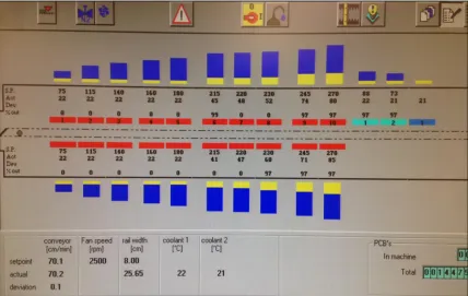
atmosphere with an oxygen level of less than 50ppm.
The reflow process was designed to heat the specimens at a rate of 480C per minute from
room temperature to a peak temperature of 2400C to 2440C before cooling at a rate of
570C per minute. Total time above liquidus (TAL, 2170C) was approximately 45 seconds,
shown in Figure 19.
Figure 19 Reflow Profile
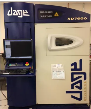
The samples were then inspected using electrical resistance readings and x-ray imaging to
35
When a solder joint location was identified as electrically open after reflow processing,
the corresponding paste volume was determined from the SPI data and classified as
‘insufficient’. Ultimately, the largest paste deposit resulting in a non-functional solder
joint was then used to define the minimum acceptable deposit volume for each
component type.
After the minimum acceptable deposit volume has been determined, Successful (i.e.
electrically good) component to motherboard assemblies were subjected to an accelerated
thermal cycle environment using a Thermotron F-110 chamber. The thermal profile
developed for this experiment systematically cycled between ˗400C and 1250C with 15
minute dwell times maintained at the temperature extremes. Temperature transition rates
were between 60C and 70C per minute resulting in a total cycle time of 80 minutes, see
36
Figure 20 Thermal Cycling profile -400C to 1250C
3.3 Test Vehicle
The test vehicles utilized in this experiment were constructed using stitch patterned
motherboard footprints and mating dummy surface mount devices. When successfully
reflow soldered, these vehicles produced continuous daisy-chains that allowed for simple
electrical testing of the newly created first level solder joint interconnections.
The boards were constructed using 370HR laminate. Each board contained eight copper
layers and had a total mask to mask thickness of 2.5mm. Each copper layer was formed
37
Layers 1 and 8 were used for signal transmission while inner layers 2 through 7 were
non-functional dummy planes.
The boards were acquired with immersion gold over electroless nickel (ENIG) or copper
OSP surface finishes. Each board was mechanically routed to include multiple coupons
each containing one or more footprints for surface mount device attachment. In addition
to input and output traces, each footprint also contained probe points to facilitate failure
location isolation with an ohm-meter. For this experiment, two LGA, two QFN and two
BGA designs were evaluated.
Figure 21 Test Vehicle bare board Cu-OSP surface finish
LGA 208
LGA 97
QFN 100
QFN 156
38
Figure 22 Test Vehicle Assembled
3.4 Package Types
For this experiment LGA 208, LGA 97, QFN 100, QFN 156, BGA 144 and BGA 360
were evaluated. All components were dummy components and acquired from practical
components.
3.4.1 Land Grid Array (LGA) 208
Figure 23.LGA 208 ENIG, Cu-OSP surface finish coupons and component bottom side
LGA 208
QFN 100
QFN 156
LGA 97
BGA 144
BGA 360
39
The LGA208 device was a 15x15mm component consisting of 208 I/O arranged at
0.8mm pitch using a 17x17 depopulated array pattern. The component attachment pads
were defined by mask openings of 0.4mm in diameter and were finished with gold over
nickel (Ni/Au) plating.
The LGA208 motherboard footprint pads measured 0.376mm in diameter and were
defined by mask openings of 0.5mm (i.e. solder mask defined geometry).
Due to limited sample size only LGA 208 was evaluated on both ENIG and Cu-OSP
surface finishes.
3.4.2 Land Grid Array (LGA) 97
Figure 24 Cu-OSP surface finish coupons and component bottom side
The LGA97 component is a 5x5mm package containing 97 attachment pads arranged at
0.4mm pitch using a 10x10 depopulated array pattern. The component pads are Ni/Au
finished and solder mask defined with exposed diameters of approximately 0.2mm.
The matching LGA97 motherboard land pattern contains attachment pads that measure
40
3.4.3 Quad Flat No Lead (QFN) 100
Figure 25 Cu-OSP surface finish coupons and component bottom side
The QFN100 component was a 12x12mm package containing a perimeter array of 100
attachment pads spaced at 0.4mm pitch and an exposed thermal die paddle. The
attachment pads were bullet shaped and measured approximately 0.6x0.2mm while the
thermal die paddle measured 6.9x6.9mm. The device was acquired with a matte Sn
surface finish.
Due to the fine pitch of the device, the QFN100 motherboard pads were non-solder mask
defined by using a mask trench design (i.e. no mask between pads). Nominal pad size
was 0.25x0.78 mm. Four large pads, each measuring 3.8x3.8mm were included on the
41
3.4.4 Quad Flat No Lead (QFN) 156
Figure 26.QFN156 Cu-OSP surface finish coupon and component bottom side
The QFN156 is a dual row device consisting of 156 I/O arranged at 0.5mm pitch. The
component measures 12x12mm and contains a large thermal die paddle. The attachment
lands measure approximately 0.2x0.4mm with the inner row pads being oval in shape and
the outer row pads being bullet shaped. The exposed die paddle measures 8.9x8.9mm.
The device was procured with a matte Sn finish.
All QFN156 motherboard attachment pads were bullet shaped, measuring 0.27x0.44mm.
The pads were non-solder mask defined using 0.05mm mask clearance per side. The
center of the footprint contains four large pads for die paddle soldering, each measuring
42
3.4.5 BGA 144
Figure 27 BGA 144 Cu-OSP surface finish coupon and component bottom side
BGA 144 footprint for a 144 I/O BGA. The attachment pads measure 0.38mm in
diameter and are non-solder mask defined. Mask openings are 0.6mm diameter.
The BGA 144 component was a 13x13mm package containing a grid array of 144 ball
attachment with a pitch of 1mm. It had a silicon die measuring approximately 10x10mm
and 0.3mm thick.
3.4.6 BGA 360
Figure 28 BGA 360 Cu-OSP surface finish coupon and component bottom side
BGA 360 footprint for a 360 I/O BGA. The attachment pads measure 0.3mm in diameter
43
The BGA 360 component was a 10x10mm package containing a grid array of 360 ball
attachment with a pitch of 0.4mm. It had a silicon die measuring approximately 5x5mm
and 0.3mm thick.
3.5 Stencil Designs
All stencils used for this study were fabricated using 4mil thick stainless steel foil and cut
using laser technology.
In order to evaluate the minimum solder paste deposit volume required to both form a
good electrical connection and a reliable solder joint, two or three undersized aperture
sizes were designed into the stencil foils for each device type. These undersized apertures
targeted transfer efficiencies of 30, 40 and 50% for BGA and QFN components and TE
of 60, 75 and 80% for the LGA devices. Additionally, an oversized aperture targeting
120% TE was included for the LGA208 component. A summary of the standard and
44
Table 4 Summary of stencil designs
The position of each undersized or oversized aperture was chosen based on package
construction and/or existing failure analysis information acquired from an earlier
assembly and a -400C to 1250C accelerated thermal cycling (ATC) experiment using
similar components and test board footprints.
For the LGA devices, four undersized aperture positions were included in each stencil
45
outermost solder joint position and three solder joint positions arranged beneath the
package die shadow region (Figure 29 and Figure 30). The outermost positions were
chosen because both devices historically showed a tendency to fail due to corner joint
solder fatigue during thermal cycling. The die shadow positions were chosen because
solder joint failure in the die shadow region may occur under certain conditions, such as
the formation of an undersized solder joint. For LGA 208, an additional design with
oversized joints was included to test the effect of oversize solder deposits in ATC (Figure
31). In this instance, the oversized solder deposits were placed at the corner most joint
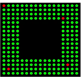
positions.
[image:57.612.242.406.325.481.2]Figure 29 LGA 208 stencil aperture layout. Green indicates standard stencil aperture positions, red indicates undersized aperture positions.
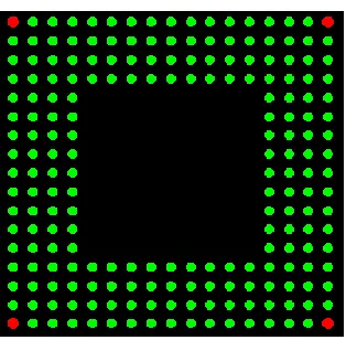
46
Figure 31 LGA 208 stencil aperture layout. Green indicates standard stencil aperture positions, red indicates oversized aperture positions.
For the QFN components, the undersized apertures were placed at the corner most solder
joint positions, which had been found to fail earliest in thermal cycle testing. In the case
of the QFN100, this design amounted to eight undersized apertures whose positions are
shown in Figure 32.
Figure 32 QFN 100 stencil aperture layout. Green indicates standard stencil aperture positions, red indicates undersized aperture positions.
With the dual-row QFN156 the undersized apertures were included at the 16 corner most
solder joint positions shown in Figure 33, which were believed to be the most susceptible
[image:58.612.239.409.382.533.2]47
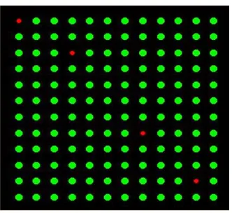
Figure 33 QFN 156 stencil aperture layout. Green indicates standard stencil aperture positions, red indicates undersized aperture positions.
For the BGA 144 component, four undersized apertures were placed alone the diagonal
with one undersized aperture at the North-West corner solder joint position and the other
three undersized apertures in the inner rows as shown in Figure 34 .
Figure 34 BGA 144 stencil aperture layout. Green indicates standard stencil aperture positions, red indicates undersized aperture positions.
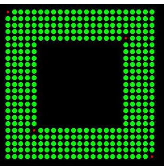
For the BGA 360 component, four undersized apertures were placed alone the diagonals
with two undersized apertures one at the North-West corner solder joint position and one
at South- East corner joint position and the other two undersized apertures were in the
[image:59.612.242.408.389.541.2]48
Figure 35 BGA 360 stencil aperture layout. Green indicates standard stencil aperture positions, red indicates undersized aperture positions.
3.6 Equipment and process setting
All the assembly build and experimental testing was done at Universal Instruments
Advanced Processing Lab (APL).
3.6.1 Stencil Printer
[image:60.612.242.409.68.235.2]A DEK stencil printer was used. With the following printing parameters:
49 Printing Pressure = 12 kg
Printing Speed = 10mm/sec
Separation Speed = 2.0mm/sec
600 angle squeeze
All boards were fully supported and contact printed (i.e., zero standoff) No standoff is
used it was a contact printing process. Same settings were used to maintain steady
process.
3.6.2 Solder Paste Inspection System
SPI is an automated visual inspection of printed circuit board (PCB), where cameras at
different angles autonomously scans the PCB under test for solder paste printing defects.
A Koh Young KY8030-3 SIP system was used to screen the solder paste deposits. The
system was programed to measures the height, area and volume of the solder paste
deposit printed during the stencil printing process. For initial assemble yield test all the
50
Figure 37 Solder Inspection System
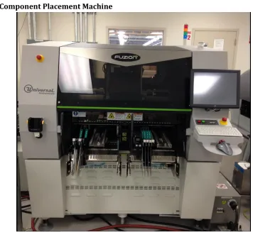
3.6.3 Component Placement Machine
[image:62.612.136.492.331.658.2]51
Component placement machine also known as pick and place machine are used for high
speed and accurate assemblies. A FUZION component placement machine was used to
populate the PCB board. Components were fed to the machine using matrix trays. The
machine had an In-line 7 head, a program for the test board was created using the PCB
design dimensions. The machine picks the components using vacuum nozzles and places
it exact on its foot print on the board using alignment and vision systems. It uses high
resolution cameras to identify the components and inspect them to find any damage or
missing features.
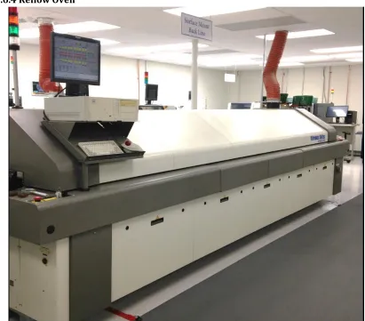
[image:63.612.114.525.310.671.2]3.6.4 Reflow Oven