Theses Thesis/Dissertation Collections
3-2018
The Design of a Debugger Unit for a RISC
Processor Core
Nikhil Velguenkar
[email protected]Follow this and additional works at:http://scholarworks.rit.edu/theses
This Master's Project is brought to you for free and open access by the Thesis/Dissertation Collections at RIT Scholar Works. It has been accepted for inclusion in Theses by an authorized administrator of RIT Scholar Works. For more information, please [email protected].
Recommended Citation
The Design of a Debugger Unit for a RISC Processor Core
by
Nikhil Velguenkar
Graduate Paper
Submitted in partial fulfillment of the requirements for the degree of
Master of Science
in Electrical Engineering
Approved by:
Mr. Mark A. Indovina, Lecturer
Graduate Research Advisor, Department of Electrical and Microelectronic Engineering
Dr. Sohail A. Dianat, Professor
Department Head, Department of Electrical and Microelectronic Engineering
Department of Electrical and Microelectronic Engineering Kate Gleason College of Engineering
Rochester Institute of Technology Rochester, New York
Abstract
Declaration
I hereby declare that except where specific reference is made to the work of others, the contents of this paper are original and have not been submitted in whole or in part for consideration for any other degree or qualification in this, or any other University. This paper is the result of my own work and includes nothing which is the outcome of work done in collaboration, except where specifically indicated in the text.
I would like to thank my advisor, Mark Indovina for guiding me throughout the project, and also during the coursework at RIT which helped me build practical design concepts along with theoretical approach. Through his courses and labs I was able to convert complex design ideas into working implementation which I take with me as a valuable skill learned at RIT.
Contents
Abstract ii
Declaration iv
Acknowledgements v
Contents vi
List of Figures viii
List of Listings ix
List of Tables x
1 Introduction 1
1.1 Need for Debugging Instrumentation . . . 3
1.2 Debugging Approach . . . 5
1.2.1 Hardware Triggering and Trace . . . 5
1.2.2 In-Circuit Emulator . . . 7
1.2.3 Communication-Centric Debug . . . 7
1.2.4 Scan Chain Based Debug . . . 8
1.2.5 Run-Stop Based Debugging . . . 8
2 Design for Debug 10 2.1 Communication Interface . . . 12
2.2 Core Instrumentation . . . 13
2.2.1 Processor Specific Controls . . . 13
2.2.2 Reading Processor Internal State . . . 15
2.2.3 Memory Read-Write . . . 15
2.2.4 Trace Data . . . 16
3 Hardware Instrumentation For Debugging 18
3.1 ARM Debugging Instrumentation . . . 18
3.2 Intel Trace Instrumentation[1] . . . 20
4 Design Implementation 21 4.1 Design Components . . . 22
4.1.1 AMBER 25 Core . . . 23
4.1.1.1 IP Instrumentation . . . 23
4.1.2 Test Access Port & JTAG . . . 25
4.1.3 Debug Module . . . 27
4.2 Design Implementation . . . 27
4.2.1 JTAG Instructions Implementation . . . 31
4.2.1.1 Read CPU State . . . 31
4.2.1.2 Store Breakpoint . . . 31
4.2.1.3 Memory Access . . . 32
4.2.1.4 Trace Data . . . 32
5 Tests and Results 33 5.1 JTAG Instructions . . . 33
5.1.1 Run and Stop . . . 33
5.1.2 Memory Access . . . 34
5.1.3 Trace . . . 35
5.2 System Overhead . . . 35
5.2.1 Area Overhead . . . 35
5.2.2 Power Overhead . . . 36
6 Conclusions 39 6.1 Future Work . . . 40
References 42
List of Figures
2.1 JTAG TAP Overview [2] . . . 12
2.2 Test Access Port Controller State Machine[3] . . . 14
4.1 System Overview . . . 22
4.2 Amber Processor 5 Stage Pipeline[4] . . . 24
4.3 Halt Core Logic . . . 25
4.4 State Read Internal Register . . . 26
4.5 JTAG Module . . . 26
4.6 Debug State Machine . . . 28
4.7 Debug Module Logical View . . . 29
4.8 Debug Module . . . 29
4.9 Complete System . . . 30
5.1 Stop and Read State . . . 33
5.2 Send CPU State Date . . . 34
5.3 Memory Read . . . 34
I.1 Debug Module Header . . . I-1
I.2 Debug Module . . . I-3
List of Tables
5.1 Area Overhead . . . 36
5.2 Area Distribution For Complete System With Debug Module . . . 36
5.3 Power Overhead, Post Scan Netlist . . . 36
5.4 Power Overhead, Pre-Scan Netlist . . . 37
Introduction
Embedded Systems Design consists of both hardware and software, commonly known as firmware, that mostly operate and control in a standalone manner. The Embedded Sys-tems market has seen a significant increase since almost every electronic device includes
an microprocessor. According to the Zion market research report, “Embedded Systems
Market (Embedded Hardware and Embedded Software) Market for Healthcare, Industrial,
Automotive, Telecommunication, Consumer Electronics, Defense, Aerospace and Others
Applications: Global Industry Perspective, Comprehensive Analysis and Forecast, 2015
-2021” embedded systems market would generate a revenue almost double by 2021. This
2
and validating those features thus reducing the gap between debugging infrastructure and corresponding hardware designs. This in-turn would reduce bugs in silicon and effort put into re-spins. A proper and powerful debugging infrastructure will help designers to design first time right silicon. This chapter further explains the need for debugging instrumen-tation and evolution of debugging practices. Later, the paper covers a research literature survey and describes the Design for Debug methodology in Chapter 2. Chapter 3 goes through various debugging infrastructures. Chapter 4 discusses the design and implemen-tation in this project. Chapter 5 discusses the results of the implemenimplemen-tation and Chapter 6 concludes the project and lists its future scope. Finally, the Appendix includes listing of source code for designed Debug Module.
1.1
Need for Debugging Instrumentation
impor-1.1 Need for Debugging Instrumentation 4
tant to understand that if there are bugs, we cannot fix anything that is not visible[2].
to some extent uses features which are instrumented in the core for debugging purposes. Embedded Systems debugging can be divided in two types namely: stop and halt approach, and real time trace approach. For real-time Embedded Systems sometimes it not possible to halt and debug as this might cause the program to malfunction, due to the fact that serving deadlines is one of the important task for real-time Embedded Systems, hence real time trace dump data is read while debugging these systems. Trace dump is the data which captures trace for any configured signal and is stored while program is running without halting the processor. This stored trace data can be accessed over debugging port. This mechanism helps to find what was the CPU state or instructions that were executed over time. Overall these are major requirements for a debugging environment in real-time Em-bedded Systems which can be addressed via instrumentation of an on-chip debugger unit which communicate with any compatible external device using communication interface such as JTAG, Serial Wire Debug (SWD), etc.
1.2
Debugging Approach
Explained below are various debugging approaches which evolved over time and are cur-rently used by different processor architectures. There are advantages and disadvantages of the various approaches depending upon requirements. Implementing any debugging methodology is not straight forward as it depends upon needs and requirements along with trade-off for performance and accessibility.
1.2.1
Hardware Triggering and Trace
1.2 Debugging Approach 6
1.2.2
In-Circuit Emulator
An In-Circuit Emulator (ICE) has long been used for debugging hardware designs and has evolved over time. It typically uses an external hardware device connected to or in place the chip under test. This hardware emulates complete functionalities of the chip under test with many additional features to read its internal state and signals. In the early days of in-circuit emulation, the test processor was replaced with a special debugging version of the processor that has debug logic and many signals taken out of chip in-order to read using an external device. The special version of the processor was created due to the fact that the debugging instrumentation would take a large area in silicon and was to expensive to put into production silicon. These devices were typically very large as special hardware is required to emulate the device under test. This method was very powerful as it would provide a detailed view of internal signals for a chip. In fact in-circuit emulator would address nearly all aspects of the debugging requirements right from stop and read state to monitoring bus activity or trace for the processor. Now-a-days in-circuit emulators with limited features are being fabricated inside chip.
1.2.3
Communication-Centric Debug
1.2 Debugging Approach 8
and can be used as a bus analyzer.
1.2.4
Scan Chain Based Debug
Scan chains are connected to all flip flops which are used for manufacturing test for high observability and controllability of the design are inserted into a design as part of an overall Design For Test (DFT) methodology. These scan chains allow controlling internal state of the flip flops in the design during manufacturing test. This scan chain infrastructure can be re-used for accessing various hardware IPs through debugging port. Commonly used debugging ports such as JTAG based TAP or SWD. Scan chains can help extract complete state of an SoC by individually selecting IP through JTAG instructions that connects scan chain in and out path for reading state registers. It can also be used to modify data as required. This approach requires much less instrumentation of the hardware as it reuses the DFT scan chains. Implementation of TAP controller for JTAG instructions to access the scan chains in different modes of operation would consume some extra hardware overhead. This approach operates in debug mode and connects the scan chain to read the current state of the processor.
1.2.5
Run-Stop Based Debugging
Chapter 2
Design for Debug
2.1 Communication Interface 12
Figure 2.1: JTAG TAP Overview [2]
2.1
Communication Interface
The communication interface is a point of contact for an external device to talk with the internals of the hardware. Using this interface, required data inside the chip can be read by an external host for further debugging and analysis of currently executed operation or the one’s executed previously. Widely accepted standard for such an interface is JTAG which uses a TAP controller defined by IEEE Std 1149.1-2013. A JTAG interface has five pins including optional negative edge triggered reset pin. The pins include clock (TCK), test mode signal (TMS) for changing the mode, test data in (TDI) for sending test data serially, test data out (TDO) for receiving output serially and negative edge triggered reset (nTRST). The TAP controller is implemented as a state machine as defined in the IEEE
[image:24.612.140.495.118.371.2]As shown, the JTAP TAP includes two main registers: instruction register and data register. For the instruction register and data register, the values are shifted serially in using shift IR or shift DR mode and latched into the register in update DR or update IR mode. There are also proprietary standards which are followed by various chip manufacturer such as ARM, Atmel and so on, for communication and debug interface. Some of the commonly known type are ARM’s SWD and Atmel’s Program and Debug Interface (PDI). Both of these are two wire interfaces with clock and data pins; as compared to JTAG which is a five wire interface, this indeed helps in reducing external pin count. ARM’s CoreSight debugging infrastructures offers SWJ-DP which is a common interface for JTAG and SWD compatible target device. As only the JTAG interface is open and widely documented in the public domain this project uses the JTAG defined TAP controller as a communication
interface with the internal system. Figure 2.2 shown below shows the standard TAP
controller state machine as defined in IEEE Std 1149.1-2013.
2.2
Core Instrumentation
Core Instrumentation is a set of features designed into hardware in-order to modify it to read debug data from an external host device. This mainly addresses four items: processor specific controls, accessing processor internal state, read memory data, and signal trace which are required for debugging Real-Time Embedded Systems.
2.2.1
Processor Specific Controls
2.2 Core Instrumentation 14
[image:26.612.111.504.167.617.2]which in turn stalls the core. Stalling the core can be performed by gating the clock, but there is high possibility that this would result in meta-stability if stalling logic is not performed properly. Alternatively processor can be stalled by forcing it in not ready state. For a pipelined processor it is required to stall all the stages of the processor in order to avoid malfunction.
2.2.2
Reading Processor Internal State
This procedure is targeted to identify what operations are performed by a processor and, are that the results are generated as desired. It is performed by accessing internal state, i.e values from internal registers, status registers and special purpose registers after every instruction execution or at a required program counter value. These results can be used to validate with expected values. This data can be read using an internal register file after halting the core so that no further instructions are executed. Reading values at that instant and then again resuming the processor further would help identify where the malfunction occurred. This type is often classified as run stop approach.
2.2.3
Memory Read-Write
2.3 Firmware Based Debugging 16
accepted values. For processors using cache, debugging with memory access should make sure that the data in the memory is in coherence with the latest values which might be in cache. Some embedded processor provides a means to disable cache while debugging.
2.2.4
Trace Data
Trace is one of the most important feature used for debugging real-time applications. Many SoC’s include a Debug and Trace Unit which handles various trigger events like exceptions from multiple clock domain signals, unhandled exceptions, branching instructions and so on. Based on this trigger, trace probe captures the signals at various clock cycles and stores it in the on-chip trace memory. Trace produces a lot of data in real-time, thus increasing bus activity, and due to this most of the complex SoC debugging infrastructures use a different bus for reading and writing trace information. As this results in huge data on chip, a compression unit is used along with Debug and Trace Unit so as to reduce the size of the data stored and transferred. This data can be read through a communication port such as JTAG, SWD, and so on. Lower end versions of embedded processors often have no or a limited version of the trace functionality such as the ability to only trace instruction execution.
2.3
Firmware Based Debugging
Chapter 3
Hardware Instrumentation For
Debugging
Hardware instrumentation for various micro-controller based platform such as x86 from Intel, Cortex series from ARM, AVR series from Atmel, MSP 430 from Texas Instruments, PIC from Microchip, and so on, have different implementations for various debugging features. Although not all the implementations are openly accessible, instrumentation with respect to features point view in ARM’s CoreSight is very powerful, widely used, and is a well documented debugging infrastructure. This chapter discusses its features and relevancy with Design for Debug infrastructure. Note that Intel uses mostly a software based debugging approach since x86 platform.
3.1
ARM Debugging Instrumentation
3.2 Intel Trace Instrumentation[1] 20
3.2
Intel Trace Instrumentation[
1
]
Intel’s x86 architecture has been around for quite some time, but little used for light weight Embedded Systems. Debugging x86 systems normally used ICE based systems, and starting with 8086 architectures it uses firmware based debugging approach where
debugging is done by setting and reading debugging registers[1]. Now-a-days modern x86
Design Implementation
4.1 Design Components 22
4.1
Design Components
The design components of the system are shown below in the Figure 4.1. The host can be
computer or any other device which is able to send commands through JTAG interface on Debug Access Port. The JTAG interface is a standard TAP controller as defined in IEEE
Std 1149.1-2013. The Figure4.1 shows logical view of complete design implementation of
the system.
Figure 4.1: System Overview
The System on Chip shown in the Figure 4.1 is synthesizable HDL module containing
[image:34.612.146.467.260.463.2]Wishbone arbiter to arbitrate between different masters and slaves. All the components of design are explained further in following sections.
4.1.1
AMBER 25 Core
The AMBER 25 Core is an ARM v2a compatible RISC processor core. It has two variants a 3-stage pipeline (A23) and 5-stage pipeline (A25), this project uses the A25 core. The A25 includes a 32-bit datapath, and separate instruction and data caches that can be
configurable to either 2,3,4 or 8 way and each way of 8kB. As shown in the Figure 4.2,
the A25 implementation has a five stage pipeline: (i) Instruction fetch - executed at first
machine cycle used to load instruction from the main memory or cache; (ii) Decode
-executed after fetch stage used by the core to decode the instruction; (iii) Execute
-this stage process the instruction and performs operation defined in the instruction; (iv)
Memory - this stage performs memory access if required; (v) write back - this stage writes
the result to the destination location. Apart from the current design following modifications
discussed in Section 4.1.1.1 are been made for instrumenting the IP for debug purpose.
4.1.1.1 IP Instrumentation
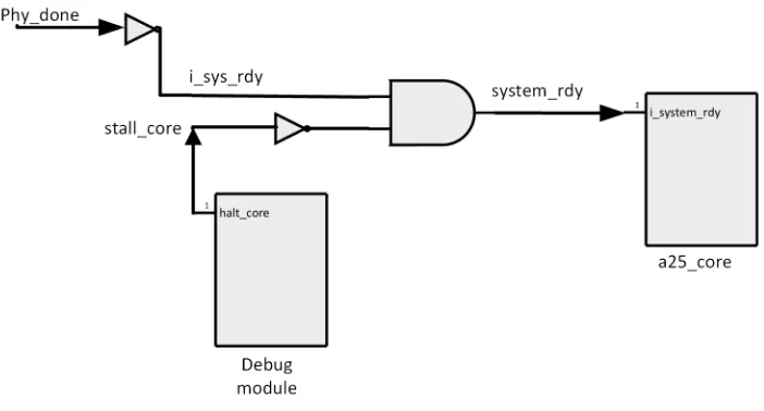
IP Instrumentation refers to the changes made in the IP in-order to communicate and control execution using the Debug Module. In order to halt the core, this design uses
i_system_rdy signal from the core which when low, halts the system at fetch stage.
i_system_rdy is used by the core for determining whether the core is ready start and
all physical interfaces and memories connected are initialized. The stalling of the fetch stage further leads to stalling of other subsequent stages in the pipeline and thus halting the core. This signal is used by the debug module for controlling the program flow of
4.1 Design Components 24
[image:36.612.217.447.143.620.2]Figure 4.3: Halt Core Logic
processor is stalled in debug mode. Internal register values are read from the register file after halting the processor. The register values are multiplexed over 32 bit bus, based on
5 bit control signal. Figure 4.4 shows the reading process. The Debug Module controls
the Multiplexer (MUX) output bystate_read_control_signal and reads the corresponding
register data over o_debug_reg_bus.
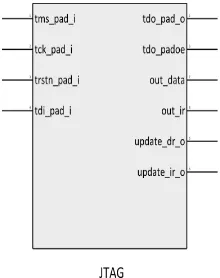
4.1.2
Test Access Port & JTAG
TAP controller is implemented as a state machine described in the IEEE Std 1149.1-2013
and in Figure 2.2 with instruction and data register. Instruction register holds the value
of instruction which is captured serially over Test Data In pin in shift_ir state and latched
to the IR register in update_ir state. Signals out_data and out_ir are 32 bit and 4
bit respectively which are used to communicate with Debug Module. As an instruction
is latched it sends it over out_ir with update_ir_o which acts as a strobe for Debug
[image:37.612.134.485.103.292.2]4.1 Design Components 26
Figure 4.4: State Read Internal Register
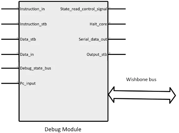
[image:38.612.183.430.144.337.2] [image:38.612.251.361.479.618.2]4.1.3
Debug Module
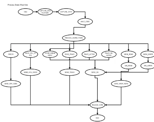
Debug Module is mainly responsible for controlling the core according to instructions
received over JTAG interface. Figure 4.6 shows state diagram of the state machine
im-plementation and Figure 4.8 shows the pin-out of the debug module with left side are
input pins and right side are output pins and Figure 4.7 shows logical view of the debug
module. State machine acts as control unit which controls different units of the design.
instruction_in and data_in are 32 bit signals which receives 32 bit instruction and
data value from JTAG module. debug_state_bus is an 32 bit input bus over which core
sends value of the internal registers. As core sends multiplexed data ondebug_state_bus,
state_read_control_signal is 5 bit output used to send control signals that corresponds to
the register value which are to be read over debug_state_bus. halt_core is the controlling
signal to stall the processor. serial_data_out and output_stbare connected totdo_pad_o
and tdo_padoe_o respectively which sends serial data off-chip.
4.2
Design Implementation
Apart from A25 core, the system has peripherals like interrupt controller, Universal Asyn-chronous Transmitter Receiver (UART), timer, boot memory, and test module. All the modules communicate via Wishbone bus. The A25 core is a Wishbone master while re-maining modules of the IP are configured as slaves. The Wishbone arbiter decides how a master selects and communicates with a slave. The complete system is designed as shown in Figure 4.9.
4.2 Design Implementation 28
[image:40.612.74.575.184.581.2]Figure 4.7: Debug Module Logical View
[image:41.612.114.503.157.347.2] [image:41.612.164.451.451.664.2]4.2 Design Implementation 30
[image:42.612.149.466.213.559.2]Debug Module. These commands execute as shown in the state diagram in Figure4.6. The design uses various aspects which were discussed in previous Chapters such as run stop debugging, memory access and trace. Along with real-time performance, area is also a very important factor when it comes to Embedded Systems, hence the added debugging logic should not take up more significant area as compared to processor logic and communication interface. Hence it is identified that run stop, trace and memory accesses are the minimum requirements for efficient debugging in this system.
4.2.1
JTAG Instructions Implementation
4.2.1.1 Read CPU State
Instruction (0101)b or (5)d can be used for read CPU state. This stage triggers a counter
values from 0 to 32 which is send over state_read_control_signal and read back over
debug_state_bus with the register values corresponding to the counter values. The data
read over debug_state_bus is stored in array of registers. Later the stored register values
in register array are send serially out onserial_data_out. output_stbremains high as long
as valid data is available on serial_data_out.
4.2.1.2 Store Breakpoint
Instruction (0111)b or (7)d can be used for storing a breakpoint. Only one breakpoint is supported and this can be stored using (7)d instruction and data register which contains the program counter value for the breakpoint which is needed to be set. The debug module continuously compares current program counter input and stored breakpoint value, on
hitting the stored breakpoint it generates halt_core which puts the processor into halt
4.2 Design Implementation 32
state instruction. The return value received for this instruction is 32’h80000001 when everything is good, else 32’hff00ff00 for error condition.
4.2.1.3 Memory Access
Instruction (0011)b or (3)d can be used for reading memory locations where in 32 bit memory location address is provided by the data register. For memory access, debug module puts the processor in halt state and communicates directly acting as a wishbone master with the memory over wishbone bus. For read memory, data is send back serially through JTAG. This only supports single location for memory read and not block memory read.
4.2.1.4 Trace Data
There are three instructions that supports trace operation namely trace read, trace log active and trace log de-active. Trace read (0110)b or (6)d is used for reading the trace
data from the memory and sending overserial_data_out signal. Trace memory is designed
as an array of 32 bit register memory. Trace log when active stores the program counter value when there is branch in program flow. Branching can be detected by comparing current program counter with previous program counter. If the current program counter is greater than four as compared to the previous one, it can be concluded that it has taken a branch. The record of theses branching instruction is stored in the memory and are
send out using serial_data_out signal on trace read command. Trace log active is set
Tests and Results
This section discusses results for the various tests performed on the debug module. Results are captured as two different types: testing JTAG instructions and identifying system overhead due to added debug module logic.
5.1
JTAG Instructions
5.1.1
Run and Stop
Figure 5.1: Stop and Read State
Figure5.1 shows stop and read CPU state, count_debug_stb is the control signal to read
[image:45.612.76.534.509.615.2]5.1 JTAG Instructions 34
which contains values for internal register that corresponding to count_debug_stb. These
are stored in the array of memory and are send serially which can be seen in Figure 5.2.
Figure 5.2: Send CPU State Date
5.1.2
Memory Access
Figure 5.3: Memory Read
Figure5.3 shows the memory read operation of the debugger. out_data is the breakpoint
address received from JTAG interface. pc_input is the program counter value which is
halted at the same point as stored breakpoint. mem_data_read is 128 bit value from the
wishbone memory read and depending upon bank selectedmem_read_data sends valid 32
bits over serial_data_out serially. halt_core is debug module output signal which halts
[image:46.612.91.520.357.504.2]5.1.3
Trace
Figure 5.4: Read Trace Memory
The Figure 5.4 shows read trace memory. Read trace memory halts the core and sends
out trace data, this is done to so that program counter address can be set at which instant back trace of the program execution flow can be done. Trace active and de-active does not halts the core, it starts logging program counter value if it changes greater than old program counter value with an offset of 4.
5.2
System Overhead
5.2.1
Area Overhead
The design is synthesized targeting a TSMC 65 nm library using Synopsys Design Com-piler using a two pass methodology: RTL synthesis resulting in a pre-scan netlist, and Test synthesis resulting in a DFT instrumented post-scan netlist utilizing a full scan protocol. Both synthesized versions of the design for the complete system contain hard macro
imple-mentations of memories, this contributed to 1412070µm2 of are used by memories macros
in the design. The total area shown in the Table5.1are inclusive with area for the memory.
The Debug Module is dominant in area consumption as a part of instrumentation of the
core for debugging purposes. Table5.1 shows difference in area with and without debugger
[image:47.612.78.580.137.213.2]5.2 System Overhead 36
Table 5.1: Area Overhead
Module Pre-Scan (µm2)
Combinational Non-Combinational Buffer/Inv Total
Debug Module 90,301.780 134,466.394 3,925.152 224,768.174
System w/o Debug 401,596.274 347,658.6994 44,128.023 2,161,324.974
System with Debug 491,834.853 482,125.094 47,979.994 2,386,029.947
Post-Scan (µm2)
Combinational Non-Combinational Buffer/Inv Total
Debug Module 90,371.634 160,478.848 3,805.401 250,850.483
System w/o Debug 401,416.649 417,280.262 43,951.723 2,161,324.974
System with Debug 491,751.693 577,918.777 47,743.819 2,481,740.471
Table 5.2: Area Distribution For Complete System With Debug Module
Module Pre-Scan (µm2) Percentage Post-Scan (µm2) Percentage
Debug Module Total Area 224,748.216 9.4 250,950.275 10.1
Debug Module Combinational 87780.369 3.67 87,810.306 3.53
Debug Module Non Combinational 134466.394 5.63 160,638.515 6.47
Table 5.2 shows the the Debug Module increases the area post addition of scan chains
by 10.1 percent. In Table5.1 the values for Debug Module are calculated for a standalone
design, whereas Table5.2shows the distribution of the area for Debug Module synthesized
with complete system. Percentage in Table 5.2 is calculated with respect to complete
system area.
5.2.2
Power Overhead
Power overhead is shown in Table 5.3.
Table 5.3: Power Overhead, Post Scan Netlist
Module Internal Power Switching Power Total Dynamic Power Leakage Power
System w/o debug 9.6514 mW 6.9248 mW 16.5762 mW 3.3116 uW
Note that the complete system with Debug Module consumes 8.90mW more than the
one without the Debug Module. There is also a substantial increase in leakage power of
1.06uW, for a total overall increase in power consumption of 8.91mW. The results in the
Table 5.4shows pre-scan power consumption, its shows very little increase as compared to
one with scan chains.
Table 5.4: Power Overhead, Pre-Scan Netlist
Module Internal Power Switching Power Total Dynamic Power Leakage Power
System w/o debug 11.4877 mW 1.8732 mW 13.3609 mW 2.9435 uW
System with debug 17.6651 mW 2.0396mW 19.7048mW 3.8850 uW
With an increase in area, internal power is increased considerably as compared to switching power. The Debug Module can be power gated when not in use to save power consumption.
Table 5.5 shows that the increase in power consumption is dominated by use of many
Conclusions
This study discussed the importance of Design for Debug approach for hardware design of Embedded Systems and then implements debug hardware blocks to verify overhead impact on the target system design. As this study was focused on bare-metal real time embedded systems, features such as breakpoints, memory access, and trace were identified as impor-tant and a minimum requirement for debugging embedded systems. It can be observed
that for the features implemented the design with debugger increases area by about 10.1
percent as compared to one without debugger. There is a substantial increase in internal
power by about 8.9mW, mostly dominated by the use of registers. As the debugging unit
6.1 Future Work 40
techniques, it would decrease time to verify and test for various cases. In case of bugs encountered, this can be helpful to provide with internal details required to understand the root cause easily and efficiently. This would reduce overall development cycle time and also minimizing chip re-spins. As embedded systems are designed and used for variety of reasons, always having software emulation based debugging is not advisable, true on-chip debugger should be required as this gives real view of working chip internals. Although trade offs can be made depending upon area required for the debugger with what features can be implemented in hardware or what can be implemented in firmware that can be triggered for debugging purposes. Most of the features can be implemented in firmware using interrupts and triggering appropriate ISR except for instruction trace. Firmware based debugging when used will often deviate from actual program execution and would not be able to give a complete out of the box system view to the designer or user. The implementation of the features still remains a trade-off between software and hardware giving the fact that hardware adds a 10% increase to the overall system area.
6.1
Future Work
Debugger design is always evolving as new micro-architecture implementations are evolv-ing. Its capabilities will always change, update or become obsolete over time. Currently this project focused on hardware instrumentation of the core and its effect. Future scope would include compatible front end GUI for communicating with JTAG port. There are many open source implementations for front end GUI for communicating over JTAG. Open On-Chip Debugger is one of the open source projects which uses instrumented features for debugging of the core and communicates over JTAG or SWD interface and is integrated
References
[1] S. Bach, “Design and Implementation of a Debugging Unit for the OpenProcessor Platform,” Master’s thesis, University of Karlsruhe (TH) Institute of Operational and dialog systems, February 2008.
[2] N. Stollon,On-Chip Instrumentation: Design and Debug for Systems on Chip, 1st ed.
Springer Publishing Company, Incorporated, 2010.
[3] IEEE, “IEEE Standard for Test Access Port and Boundary-Scan Architecture,”IEEE
Std 1149.1-2013 (Revision of IEEE Std 1149.1-2001), pp. 1–444, May 2013.
[4] Amber Open Source Project: Amber 2 Core Specification, Mar. 2015.
[5] D. Rath, “Open On-Chip Debugger,” Master’s thesis, University of Applied Sciences Augsburg, 2005.
[6] P. Fogarty, “Minimising The Impact of Software Instrumentation Using On-Chip
De-bug and a Secondary CPU Core,” in Proceedings of the 2012 System, Software, SoC
and Silicon Debug Conference, Sept 2012, pp. 1–5.
[7] D. Leman, “Hardware-Assisted Breakpoints,” Dr.Dobb’s Journal, vol. 30, no. 6,
[Online]. Available: http://search.proquest.com.ezproxy.rit.edu/docview/202732033? accountid=108
[8] J. Backer, D. Hely, and R. Karri, “Secure and Flexible Trace-based Debugging
of Systems-on-chip,” ACM Trans. Des. Autom. Electron. Syst., vol. 22, no. 2, pp.
31:1–31:25, Dec. 2016. [Online]. Available: http://doi.acm.org.ezproxy.rit.edu/10.
1145/2994601
[9] N. Ohba and K. Takano, “Hardware Debugging Method Based on Signal Transitions
and Transactions,” in Proceedings of the 2006 Asia and South Pacific Design
Automation Conference, ser. ASP-DAC ’06. Piscataway, NJ, USA: IEEE Press,
2006, pp. 454–459. [Online]. Available: https://doi-org.ezproxy.rit.edu/10.1145/
1118299.1118412
[10] N. C. Darounkola, “Source-Level Debugging Framework Design For FPGA High-Level Synthesis,” Ph.D. dissertation, Department of Electrical and Computer
Engineering University of Toronto, 2014. [Online]. Available: http://search.proquest.
com.ezproxy.rit.edu/docview/1648982034?accountid=108
[11] M. Sami, M. Malek, U. Bondi, and F. Regazzoni, “Embedded Systems Education:
Job Market Expectations,” SIGBED Rev., vol. 14, no. 1, pp. 22–28, Jan. 2017.
[Online]. Available: http://doi.acm.org/10.1145/3036686.3036689
[12] G. Stringham, Hardware/Firmware Interface Design, Best Practices for Improving
Embedded Systems Development. Elsevier Science, 2009. ProQuest Ebook Central,
2009. [Online]. Available: https://ebookcentral.proquest.com/lib/rit/detail.action?
References 44
[13] H. P. E. Vranken, M. P. J. Stevens, and M. T. M. Segers, “Design-For-Debug in
Hard-ware/Software Co-Design,” inHardware/Software Codesign, 1997. (CODES/CASHE
’97), Proceedings of the Fifth International Workshop on, Mar 1997, pp. 35–39.
[14] H. F. Ko, A. B. Kinsman, and N. Nicolici, “Design-for-Debug Architecture for
Dis-tributed Embedded Logic Analysis,”IEEE Transactions on Very Large Scale
Integra-tion (VLSI) Systems, vol. 19, no. 8, pp. 1380–1393, Aug 2011.
[15] K. G. Bart Vermeulen,Debugging Systems-on-Chip. Springer, Cham, 2014.
[16] E. A. A. Daoud, “On-Chip Debug Architectures For Improving Observability During Post-Silicon Validation,” Ph.D. dissertation, McMaster University, 2008.
[17] A. Kourfali and D. Stroobandt, “Efficient Hardware Debugging Using Parameterized
FPGA Reconfiguration,” in 2016 IEEE International Parallel and Distributed
Pro-cessing Symposium Workshops (IPDPSW), May 2016, pp. 277–282.
[18] Y.-H. Im, S.-J. Nam, B.-W. Kim, K.-G. Kang, D.-H. Lee, J.-H. Yang, Y.-S. Kwon, J.-H. Lee, and C.-M. Kyung, “Co-development of Media-processor and Source-level
Debugger using Hardware Emulation-based Validation,” in VLSI and CAD, 1999.
ICVC ’99. 6th International Conference on, 1999, pp. 95–98.
[19] C. R. Hill, “A Real-time Microprocessor Debugging Technique,” inProceedings of the
Symposium on High-level Debugging, ser. SIGSOFT ’83. New York, NY, USA: ACM,
1983, pp. 145–148. [Online]. Available: http://doi.acm.org/10.1145/1006147.1006179
[20] I.-J. Huang and T.-A. Lu, “ICEBERG: An Embedded In-Circuit Emulator Synthesizer
for Microcontrollers,” in Proceedings 1999 Design Automation Conference (Cat. No.
[21] M. Abramovici, P. Bradley, K. Dwarakanath, P. Levin, G. Memmi, and D. Miller, “A
Reconfigurable Design-for-Debug Infrastructure for SoCs,” in 2006 43rd ACM/IEEE
Design Automation Conference, July 2006, pp. 7–12.
[22] Y.-C. Hsu, F. Tsai, W. Jong, and Y.-T. Chang, “Visibility Enhancement for Silicon
Debug,” in 2006 43rd ACM/IEEE Design Automation Conference, 2006, pp. 13–18.
[23] K. Holdbrook, S. Joshi, S. Mitra, J. Petolino, R. Raman, and M. Wong, “MicroSPARC:
A Case-Study of Scan Based Debug,” in Proceedings., International Test Conference,
Oct 1994, pp. 70–75.
[24] A. B. T. Hopkins and K. D. McDonald-Maier, “Debug Support for Complex Systems
On-Chip: A Review,” IEE Proceedings - Computers and Digital Techniques, vol. 153,
no. 4, pp. 197–207, July 2006.
[25] B. Vermeulen and S. K. Goel, “Design for Debug: Catching Design Errors in Digital
Chips,” IEEE Design Test of Computers, vol. 19, no. 3, pp. 35–43, May 2002.
[26] A. Verge, N. Ezzati Jivan, and M. R. Dagenais, “Hardware Assisted Software Event
Tracing,” Concurrency and Computation: Practice and Experience, vol. 29, no. 10, 5
2017. [Online]. Available: https://doi.org/10.1002/cpe.4069
[27] B. Scherer and G. Horvath, “Trace and Debug Port Based Watchdog Processor,” in
2012 IEEE International Instrumentation and Measurement Technology Conference
Proceedings, May 2012, pp. 488–491.
[28] White Paper CoreSight Technical Introduction, Aug. 2013. [Online].
Avail-able: http://infocenter.arm.com/help/topic/com.arm.doc.epm039795/coresight_
Appendix I
Source Code
Listing I.1: Debug Module Header
/∗ ∗
∗ Author : N i k h i l Velguenkar
∗ Date : 1/1/2018
∗ ∗ ∗ ∗/
//−−−−−−−−−−−−−−−−−−−−−−−−−−−−−−−−−
// Process Data S t a t e Machine
//−−−−−−−−−−−−−−−−−−−−−−−−−−−−−−−−−
` d e f i n e IDLE_PROCESS 5 ' d0
` d e f i n e CAPTURE_INSTRUCTION 5 ' d1
` d e f i n e CAPTURE_DATA 5 ' d2
` d e f i n e HALT_CORE 5 ' d3
` d e f i n e PROCESS_INSTRUCTION 5 ' d4
` d e f i n e ERROR 5 ' d5
` d e f i n e READ_CPU_STATE 5 ' d6
` d e f i n e STORE_BREAKPOINT 5 ' d7
` d e f i n e READ_TRACE 5 ' d8
` d e f i n e READ_MEM 5 ' d9
` d e f i n e WB_READ 5 ' d10
` d e f i n e WB_WRITE 5 ' d12
` d e f i n e RELEASE_CORE 5 ' d13
` d e f i n e TRACE_LOG_ACTIVE 5 ' d14
` d e f i n e TRACE_LOG_DEACTIVE 5 ' d15
` d e f i n e SEND_TRACE 5 ' d16
` d e f i n e SEND_MEM_READ 5 ' d17
` d e f i n e SEND_ERR_CODE 5 ' d18
` d e f i n e SEND_CPU_STATE 5 ' d19
I-3
Listing I.2: Debug Module
/∗ ∗
∗ Author : N i k h i l Velguenkar
∗ Date : 1/1/2018
∗ De sc r ip tio n : This module i s f o r debug c o n t r o l implemented as s t a t e
∗ machine
∗ ∗/
module DebugModule (
r e s e t , clk , scan_in0 , scan_en , test_mode , scan_out0 , instruction_stb , data_stb ,
in s t ruc tio n_ in , data_in , debug_state_bus , state_read_control_signal , halt_core , serial_data_out , output_stb , pc_input , o_wb_address , o_wb_sel , o_wb_data , o_wb_we, o_wb_cyc , o_wb_stb , i_wb_data , i_wb_ack , i_wb_err // s t a t e ) ;
r e s e t , // system r e s e t c l k ; // system c l o c k
input
scan_in0 , // t e s t scan mode data input scan_en , // t e s t scan mode enable test_mode ; // t e s t mode s e l e c t
output
scan_out0 ; // t e s t scan mode data output
input
instruction_stb , // i n s t r u c t i o n read c o n t r o l s t b data_stb ; // debug data read c o n t r o l s t b
` i n c l u d e " . / i n c l u d e /DebugModule . h "
input [ 3 : 0 ] i n s t r u c t i o n _ i n ; // i n s t r u c t i o n _ r e g JTAG
input [ 3 1 : 0 ] data_in ; // JTAG data reg
input [ 3 1 : 0 ] debug_state_bus ; // s t a t e read bus
input [ 3 1 : 0 ] pc_input ; // PC v a l u e s from the core
output reg [ 4 : 0 ] state_read_control_signal ;
output reg halt_core ;
output reg output_stb ;
output reg serial_data_out ;
// output [ 4 : 0 ] s t a t e ;
//−−−−−−−−−−−−−−−−−−−−−−−−−−−−−
// wishbone i n t e r f a c i n g s i g n a l s //−−−−−−−−−−−−−−−−−−−−−−−−−−−−−
output reg [ 3 1 : 0 ] o_wb_address ;
output reg [ 1 5 : 0 ] o_wb_sel ;
output reg [ 1 2 7 : 0 ] o_wb_data ;
output reg o_wb_we ;
output reg o_wb_cyc ;
output reg o_wb_stb ;
input [ 1 2 7 : 0 ] i_wb_data ;
input i_wb_ack ;
I-5
//−−−−−−−−−−−−−−−−−−−−−−−−−−−−−−
// i n t e r n a l r e g i s t e r and wires //−−−−−−−−−−−−−−−−−−−−−−−−−−−−−−−
reg serial_done ;
reg [ 4 : 0 ] counter ;
reg [ 4 : 0 ] state_process ;
reg [ 4 : 0 ] next_state_process ;
// c o n t r o l r e g i s t e r
reg halt_done ;
reg w_halt_core ;
reg wb_read_done , wb_write_done , wb_write , wb_read ;
reg store_breakpoint_done , store_breakpoint ;
reg step_by_step ;
reg read_cpu_state , trace_active , trace_deactive ;
reg cpu_read_done ;
reg [ 3 : 0 ] count_debug_stb ;
reg [ 3 1 : 0 ] breakpoint_reg ;
reg [ 3 1 : 0 ] mem_read_data ;
//−−−−−−−−−−−−−−−−−−−−−−−−−−−−−−−−−−−−−−−−−
// Wiring
//−−−−−−−−−−−−−−−−−−−−−−−−−−−−−−−−−−−−−−−−−
// a s s i g n w_state = s t a t e ;
// a s s i g n w_serial_done = serial_done ; // a s s i g n w_read_data = data_reg ; // a s s i g n s t a t e = s t a t e_ p r oc e s s ; // a s s i g n halt_core = s_halt_core ;
//−−−−−−−−−−−−−−−−−−−−−−−−−−−−−−−−−−−−−−−−−
// Other Logic
//−−−−−−−−−−−−−−−−−−−−−−−−−−−−−−−−−−−−−−−−
// Process S t a t e
//−−−−−−−−−−−−−−−−−−−−−−−−−−−−−−−−−−−−−−−−−−−−−−−−−−−−−−−−−−−−−−−
/∗
IDLE_PROCESS : d e f a u l t s t a t e
HALT_CORE : s t a l l core
PROCESS_INSTRUCTION : process i n s t r u c t i o n
ERROR : Error S t a t e
READ_CPU_STATE : read CPU r e g i s t e r s
STORE_BREAKPOINT : hardware r e g i s t e r s to s t o r e b r e a k p o i n t
READ_TRACE : Read t r a c e data
READ_MEM : Read memory through wb i n t e r f a c e
WRITE_MEM : Write Memory through wb i n t e r f a c e
WB_READ : Read p r o t o c o l f o r wishbone i n t e r f a c e WB_WRITE : Write p r o t o c o l f o r wishbone i n t e r f a c e
SEND_CPU_STATE : Send CPU s t a t e over JTAG
SEND_TRACE : Send TRACE data over JTAG
SEND_ERR_CODE : send a code over Jtag
SEND_MEM_READ : Send Memory read Data
SEND_OK : Sends Ok error code
RELEASE_CORE : Releases core from h a l t s t a t e
∗/
reg send_cpu_state ;
reg send_err_code ;
reg send_trace ;
reg send_ok ;
reg send_mem_read ;
reg e r r o r ;
reg send_trace_done ;
reg send_mem_data_done ;
reg send_ok_done ;
reg capture_ins ;
reg capture_data ;
reg [ 3 : 0 ] i n s t r u c t i o n _ r e g ;
reg [ 3 1 : 0 ] data_reg ;
reg [ 4 : 0 ] send_count ;
reg [ 4 : 0 ] send_err_count ;
reg [ 4 : 0 ] index ;
reg [ 5 : 0 ] index_trace ;
reg [ 4 : 0 ] send_cpu_state_count ;
reg [ 4 : 0 ] done_count ;
I-7
always @(posedge clk , posedge r e s e t )
begin
i f( r e s e t == 1 ' b1 )
begin
sta te_process <= `IDLE_PROCESS ; // r e s e t c o n d i t i o n
end e l s e
begin
sta te_process <= next_state_process ;
end end
/∗
JTAG INSTRUCTIONS:
0011 b −−> MEMORY READ
0100 b −−> MEMORY WRITE
0101 b −−> READ CPU STATE
0110 b −−> READ_TRACE
0111 b −−> STORE BREAKPOINT
1010 b −−> TRACE_LOG_ACTIVE
1011 b −−> TRACE LOG DEACTIVE
∗/
always @( state_process , instruction_stb , data_stb , instruction_reg , store_breakpoint_done , count_debug_stb , index , index_trace , send_count , wb_read_done , wb_write_done , done_count , i_wb_ack )
begin
case ( state_process )
`IDLE_PROCESS: i f ( i n s t r u c t i o n _ s t b == 1 ' b1 )
next_state_process = `CAPTURE_INSTRUCTION;
e l s e
next_state_process = `IDLE_PROCESS; `CAPTURE_INSTRUCTION: i f ( data_stb == 1 ' b1 )
next_state_process = `CAPTURE_DATA;
e l s e
next_state_process = `CAPTURE_INSTRUCTION; `CAPTURE_DATA: next_state_process = `HALT_CORE;
`PROCESS_INSTRUCTION: i f ( i n s t r u c t i o n _ r e g == 4 ' b0111 ) next_state_process =
`STORE_BREAKPOINT;
e l s e i f ( i n s t r u c t i o n _ r e g == 4 ' b0101 ) next_state_process = `READ_CPU_STATE
;
e l s e i f ( i n s t r u c t i o n _ r e g == 4 ' b0110 ) next_state_process = `READ_TRACE;
e l s e i f ( i n s t r u c t i o n _ r e g == 4 ' b0011 ) next_state_process = `READ_MEM;
e l s e i f ( i n s t r u c t i o n _ r e g == 4 ' b0100 ) next_state_process = `WRITE_MEM;
e l s e i f ( i n s t r u c t i o n _ r e g == 4 ' b1010 ) next_state_process =
`TRACE_LOG_ACTIVE;
e l s e i f ( i n s t r u c t i o n _ r e g == 4 ' b1011 ) next_state_process =
`TRACE_LOG_DEACTIVE;
e l s e
next_state_process = `ERROR;
`ERROR: next_state_process = `SEND_ERR_CODE;
`SEND_ERR_CODE: i f ( send_err_count == 5 ' b11111 )
next_state_process = `RELEASE_CORE;
e l s e
next_state_process = `SEND_ERR_CODE;
`STORE_BREAKPOINT: i f ( store_breakpoint_done == 1 ' b1 ) next_state_process = `SEND_OK;
e l s e
next_state_process = `STORE_BREAKPOINT ;
`READ_CPU_STATE: i f ( count_debug_stb == 4 ' b1111 )
next_state_process = `SEND_CPU_STATE;
e l s e
next_state_process = `READ_CPU_STATE;
`SEND_CPU_STATE: i f ( index == 5 ' b10000 )
next_state_process = `RELEASE_CORE;
e l s e
I-9
`READ_TRACE: next_state_process = `SEND_TRACE;
`SEND_TRACE: i f ( index_trace == 6 ' b100000 )
next_state_process = `RELEASE_CORE;
e l s e
next_state_process = `SEND_TRACE;
`READ_MEM: next_state_process = `WB_READ;
`WB_READ: i f ( i_wb_ack == 1 ' b1 )
next_state_process = `SEND_MEM_READ;
e l s e
next_state_process = `WB_READ;
`SEND_MEM_READ: i f ( done_count == 5 ' b11111 )
next_state_process = `RELEASE_CORE;
e l s e
next_state_process = `SEND_MEM_READ;
`WRITE_MEM: next_state_process = `WB_WRITE;
`WB_WRITE: i f ( wb_write_done == 1 ' b1 )
next_state_process = `RELEASE_CORE;
e l s e
next_state_process = `WB_WRITE;
`TRACE_LOG_ACTIVE: next_state_process = `SEND_OK;
`TRACE_LOG_DEACTIVE: next_state_process = `SEND_OK;
`SEND_OK: i f ( send_count == 5 ' b11111 )
next_state_process = `RELEASE_CORE;
e l s e
next_state_process = `SEND_OK;
`RELEASE_CORE: next_state_process = `IDLE_PROCESS;
d e f a u l t: next_state_process = `IDLE_PROCESS;
endcase end
always @( state_process )
begin
case ( state_proces s ) `IDLE_PROCESS: begin
w_halt_core = 1 ' b0 ; store_breakpoint = 1 ' b0 ; read_cpu_state = 1 ' b0 ; e r r o r = 1 ' b0 ; step_by_step = 1 ' b0 ; wb_read = 1 ' b0 ; wb_write = 1 ' b0 ; t ra ce _a ct iv e = 1 ' b0 ; trace_deactive = 1 ' b0 ; serial_done = 1 ' b0 ; send_cpu_state = 1 ' b0 ; send_err_code = 1 ' b0 ; send_trace = 1 ' b0 ; send_ok = 1 ' b0 ; send_mem_read = 1 ' b0 ; capture_ins = 1 ' b0 ; capture_data = 1 ' b0 ;
end
`CAPTURE_INSTRUCTION: begin
w_halt_core = 1 ' b0 ; store_breakpoint = 1 ' b0 ; read_cpu_state = 1 ' b0 ; e r r o r = 1 ' b0 ; step_by_step = 1 ' b0 ; wb_read = 1 ' b0 ; wb_write = 1 ' b0 ; t ra ce _a ct iv e = 1 ' b0 ; trace_deactive = 1 ' b0 ; serial_done = 1 ' b0 ; send_cpu_state = 1 ' b0 ; send_err_code = 1 ' b0 ; send_trace = 1 ' b0 ; send_ok = 1 ' b0 ; send_mem_read = 1 ' b0 ; capture_ins = 1 ' b1 ; capture_data = 1 ' b0 ;
end
I-11
w_halt_core = 1 ' b0 ; store_breakpoint = 1 ' b0 ; read_cpu_state = 1 ' b0 ; e r r o r = 1 ' b0 ; step_by_step = 1 ' b0 ; wb_read = 1 ' b0 ; wb_write = 1 ' b0 ; t ra c e _a ct iv e = 1 ' b0 ; trace_deactive = 1 ' b0 ; serial_done = 1 ' b0 ; send_cpu_state = 1 ' b0 ; send_err_code = 1 ' b0 ; send_trace = 1 ' b0 ; send_ok = 1 ' b0 ; send_mem_read = 1 ' b0 ; capture_ins = 1 ' b1 ; capture_data = 1 ' b1 ;
end
`HALT_CORE: begin
w_halt_core = 1 ' b1 ; store_breakpoint = 1 ' b0 ; read_cpu_state = 1 ' b0 ; e r r o r = 1 ' b0 ; step_by_step = 1 ' b0 ; wb_read = 1 ' b0 ; wb_write = 1 ' b0 ; t ra ce _a ct iv e = 1 ' b0 ; trace_deactive = 1 ' b0 ; serial_done = 1 ' b0 ; send_cpu_state = 1 ' b0 ; send_err_code = 1 ' b0 ; send_trace = 1 ' b0 ; send_ok = 1 ' b0 ; send_mem_read = 1 ' b0 ; capture_ins = 1 ' b0 ; capture_data = 1 ' b0 ;
end
`PROCESS_INSTRUCTION: begin
wb_read = 1 ' b0 ; wb_write = 1 ' b0 ; t ra c e _a ct iv e = 1 ' b0 ; trace_deactive = 1 ' b0 ; serial_done = 1 ' b0 ; send_cpu_state = 1 ' b0 ; send_err_code = 1 ' b0 ; send_trace = 1 ' b0 ; send_ok = 1 ' b0 ; send_mem_read = 1 ' b0 ; capture_ins = 1 ' b0 ; capture_data = 1 ' b0 ;
end
`STORE_BREAKPOINT: begin
w_halt_core = 1 ' b0 ; store_breakpoint = 1 ' b1 ; read_cpu_state = 1 ' b0 ; e r r o r = 1 ' b0 ; step_by_step = 1 ' b0 ; wb_read = 1 ' b0 ; wb_write = 1 ' b0 ; t ra c e _ a c t iv e = 1 ' b0 ; trace_deactive = 1 ' b0 ; serial_done = 1 ' b0 ; send_cpu_state = 1 ' b0 ; send_err_code = 1 ' b0 ; send_trace = 1 ' b0 ; send_ok = 1 ' b0 ; send_mem_read = 1 ' b0 ; capture_ins = 1 ' b0 ; capture_data = 1 ' b0 ;
end
`READ_CPU_STATE: begin
I-13
send_cpu_state = 1 ' b0 ; send_err_code = 1 ' b0 ; send_trace = 1 ' b0 ; send_ok = 1 ' b0 ; send_mem_read = 1 ' b0 ; capture_ins = 1 ' b0 ; capture_data = 1 ' b0 ;
end
`READ_TRACE: begin
w_halt_core = 1 ' b0 ; store_breakpoint = 1 ' b0 ; read_cpu_state = 1 ' b0 ; e r r o r = 1 ' b0 ; step_by_step = 1 ' b1 ; wb_read = 1 ' b0 ; wb_write = 1 ' b0 ; t ra c e _ a c t iv e = 1 ' b0 ; trace_deactive = 1 ' b0 ; serial_done = 1 ' b0 ; send_cpu_state = 1 ' b0 ; send_err_code = 1 ' b0 ; send_trace = 1 ' b0 ; send_ok = 1 ' b0 ; send_mem_read = 1 ' b0 ; capture_ins = 1 ' b0 ; capture_data = 1 ' b0 ;
end
`ERROR: begin
capture_ins = 1 ' b0 ; capture_data = 1 ' b0 ;
end
`READ_MEM: begin
w_halt_core = 1 ' b0 ; store_breakpoint = 1 ' b0 ; read_cpu_state = 1 ' b0 ; e r r o r = 1 ' b0 ; step_by_step = 1 ' b0 ; wb_read = 1 ' b0 ; wb_write = 1 ' b0 ; t ra c e _ a c t iv e = 1 ' b0 ; trace_deactive = 1 ' b0 ; serial_done = 1 ' b0 ; send_cpu_state = 1 ' b0 ; send_err_code = 1 ' b0 ; send_trace = 1 ' b0 ; send_ok = 1 ' b0 ; send_mem_read = 1 ' b0 ; capture_ins = 1 ' b0 ; capture_data = 1 ' b0 ;
end
`WB_READ: begin
w_halt_core = 1 ' b0 ; store_breakpoint = 1 ' b0 ; read_cpu_state = 1 ' b0 ; e r r o r = 1 ' b0 ; step_by_step = 1 ' b0 ; wb_read = 1 ' b1 ; wb_write = 1 ' b0 ; t ra c e _a ct iv e = 1 ' b0 ; trace_deactive = 1 ' b0 ; serial_done = 1 ' b0 ; send_cpu_state = 1 ' b0 ; send_err_code = 1 ' b0 ; send_trace = 1 ' b0 ; send_ok = 1 ' b0 ; send_mem_read = 1 ' b0 ; capture_ins = 1 ' b0 ; capture_data = 1 ' b0 ;
end
`WRITE_MEM: begin
I-15
store_breakpoint = 1 ' b0 ; read_cpu_state = 1 ' b0 ; e r r o r = 1 ' b0 ; step_by_step = 1 ' b0 ; wb_read = 1 ' b0 ; wb_write = 1 ' b0 ; t ra c e _ a c t iv e = 1 ' b0 ; trace_deactive = 1 ' b0 ; serial_done = 1 ' b0 ; send_cpu_state = 1 ' b0 ; send_err_code = 1 ' b0 ; send_trace = 1 ' b0 ; send_ok = 1 ' b0 ; send_mem_read = 1 ' b0 ; capture_ins = 1 ' b0 ; capture_data = 1 ' b0 ;
end
`WB_WRITE: begin
w_halt_core = 1 ' b0 ; store_breakpoint = 1 ' b0 ; read_cpu_state = 1 ' b0 ; e r r o r = 1 ' b0 ; step_by_step = 1 ' b0 ; wb_read = 1 ' b0 ; wb_write = 1 ' b1 ; t ra c e _a ct iv e = 1 ' b0 ; trace_deactive = 1 ' b0 ; serial_done = 1 ' b0 ; send_cpu_state = 1 ' b0 ; send_err_code = 1 ' b0 ; send_trace = 1 ' b0 ; send_ok = 1 ' b0 ; send_mem_read = 1 ' b0 ; capture_ins = 1 ' b0 ; capture_data = 1 ' b0 ;
end
`TRACE_LOG_ACTIVE: begin
wb_write = 1 ' b0 ; t ra c e _a ct iv e = 1 ' b1 ; trace_deactive = 1 ' b0 ; serial_done = 1 ' b0 ; send_cpu_state = 1 ' b0 ; send_err_code = 1 ' b0 ; send_trace = 1 ' b0 ; send_ok = 1 ' b0 ; send_mem_read = 1 ' b0 ; capture_ins = 1 ' b0 ; capture_data = 1 ' b0 ;
end
`TRACE_LOG_DEACTIVE: begin
w_halt_core = 1 ' b0 ; store_breakpoint = 1 ' b0 ; read_cpu_state = 1 ' b0 ; e r r o r = 1 ' b0 ; step_by_step = 1 ' b0 ; wb_read = 1 ' b0 ; wb_write = 1 ' b0 ; t ra c e _ a c t iv e = 1 ' b0 ; trace_deactive = 1 ' b1 ; serial_done = 1 ' b0 ; send_cpu_state = 1 ' b0 ; send_err_code = 1 ' b0 ; send_trace = 1 ' b0 ; send_ok = 1 ' b0 ; send_mem_read = 1 ' b0 ; capture_ins = 1 ' b0 ; capture_data = 1 ' b0 ;
end
`RELEASE_CORE: begin
I-17
send_err_code = 1 ' b0 ; send_trace = 1 ' b0 ; send_ok = 1 ' b0 ; send_mem_read = 1 ' b0 ; capture_ins = 1 ' b0 ; capture_data = 1 ' b0 ;
end
`SEND_CPU_STATE: begin
w_halt_core = 1 ' b0 ; store_breakpoint = 1 ' b0 ; read_cpu_state = 1 ' b0 ; e r r o r = 1 ' b0 ; step_by_step = 1 ' b0 ; wb_read = 1 ' b0 ; wb_write = 1 ' b0 ; t ra c e _a ct iv e = 1 ' b0 ; trace_deactive = 1 ' b0 ; serial_done = 1 ' b0 ; send_cpu_state = 1 ' b1 ; send_err_code = 1 ' b0 ; send_trace = 1 ' b0 ; send_ok = 1 ' b0 ; send_mem_read = 1 ' b0 ; capture_ins = 1 ' b0 ; capture_data = 1 ' b0 ;
end
`SEND_ERR_CODE: begin
capture_data = 1 ' b0 ;
end
`SEND_TRACE: begin
w_halt_core = 1 ' b0 ; store_breakpoint = 1 ' b0 ; read_cpu_state = 1 ' b0 ; e r r o r = 1 ' b0 ; step_by_step = 1 ' b0 ; wb_read = 1 ' b0 ; wb_write = 1 ' b0 ; t ra c e _a ct iv e = 1 ' b0 ; trace_deactive = 1 ' b0 ; serial_done = 1 ' b0 ; send_cpu_state = 1 ' b0 ; send_err_code = 1 ' b0 ; send_trace = 1 ' b1 ; send_ok = 1 ' b0 ; send_mem_read = 1 ' b0 ; capture_ins = 1 ' b0 ; capture_data = 1 ' b0 ;
end
`SEND_OK: begin
w_halt_core = 1 ' b0 ; store_breakpoint = 1 ' b0 ; read_cpu_state = 1 ' b0 ; e r r o r = 1 ' b0 ; step_by_step = 1 ' b0 ; wb_read = 1 ' b0 ; wb_write = 1 ' b0 ; t ra ce _a ct iv e = 1 ' b0 ; trace_deactive = 1 ' b0 ; serial_done = 1 ' b0 ; send_cpu_state = 1 ' b0 ; send_err_code = 1 ' b0 ; send_trace = 1 ' b0 ; send_ok = 1 ' b1 ; send_mem_read = 1 ' b0 ; capture_ins = 1 ' b0 ; capture_data = 1 ' b0 ;
end
`SEND_MEM_READ: begin
I-19
read_cpu_state = 1 ' b0 ; e r r o r = 1 ' b0 ; step_by_step = 1 ' b0 ; wb_read = 1 ' b0 ; wb_write = 1 ' b0 ; t ra c e _a ct iv e = 1 ' b0 ; trace_deactive = 1 ' b0 ; serial_done = 1 ' b0 ; send_cpu_state = 1 ' b0 ; send_err_code = 1 ' b0 ; send_trace = 1 ' b0 ; send_ok = 1 ' b0 ; send_mem_read = 1 ' b1 ; capture_ins = 1 ' b0 ; capture_data = 1 ' b0 ;
end
d e f a u l t: begin
w_halt_core = 1 ' b0 ; store_breakpoint = 1 ' b0 ; read_cpu_state = 1 ' b0 ; e r r o r = 1 ' b0 ; step_by_step = 1 ' b0 ; wb_read = 1 ' b0 ; wb_write = 1 ' b0 ; t ra ce _a ct iv e = 1 ' b0 ; trace_deactive = 1 ' b0 ; serial_done = 1 ' b0 ; send_cpu_state = 1 ' b0 ; send_err_code = 1 ' b0 ; send_trace = 1 ' b0 ; send_ok = 1 ' b0 ; send_mem_read = 1 ' b0 ; capture_ins = 1 ' b0 ; capture_data = 1 ' b0 ;
end endcase
end
// Capture I n s t r u c t i o n
always @(posedge clk , posedge r e s e t )
i f ( r e s e t == 1 ' b1 )
i n s t r u c t i o n _ r e g <= 4 ' d0 ;
e l s e begin
i f ( capture_ins == 1 ' b1 )
i n s t r u c t i o n _ r e g <= i n s t r u c t i o n _ i n ;
e l s e
i n s t r u c t i o n _ r e g <= i n s t r u c t i o n _ r e g ;
end end
// Capture Data
always @(posedge clk , posedge r e s e t )
begin
i f ( r e s e t == 1 ' b1 ) data_reg <= 32 ' d0 ;
e l s e begin
i f ( capture_data == 1 ' b1 ) data_reg <= data_in ;
e l s e
data_reg <= data_reg ;
end end
//−−−−−−−−−−−−−−
// Halt
//−−−−−−−−−−−−−−
always @(posedge clk , posedge r e s e t )
begin
i f ( r e s e t == 1 ' b1 ) halt_core <= 1 ' b0 ;
e l s e begin
i f ( ( w_halt_core == 1 ' b1 ) | | ( breakpoint_reg == pc_input ) ) halt_core <= 1 ' b1 ;
e l s e i f ( ( serial_done == 1 ' b1 ) ) halt_core <= 1 ' b0 ;
e l s e
halt_core <= halt_core ;
end end
I-21
// c o n t r o l s t a t e s i g n a l
reg [ 3 1 : 0 ] r e g i s t e r _ f i l e [ 1 5 : 0 ] ;
// a s s i g n
always @(posedge r e s e t , posedge c l k )
begin
i f ( r e s e t )
state_read_control_signal = 5 ' d0 ;
e l s e
state_read_control_signal = {1 ' b0 , count_debug_stb } ;
end
always @(posedge clk , posedge r e s e t )
begin
i f ( r e s e t == 1 ' b1 ) begin
count_debug_stb <= 4 ' b0 ; r e g i s t e r _ f i l e [ 0 ] <= 32 ' d0 ; r e g i s t e r _ f i l e [ 1 ] <= 32 ' d0 ; r e g i s t e r _ f i l e [ 2 ] <= 32 ' d0 ; r e g i s t e r _ f i l e [ 3 ] <= 32 ' d0 ; r e g i s t e r _ f i l e [ 4 ] <= 32 ' d0 ; r e g i s t e r _ f i l e [ 5 ] <= 32 ' d0 ; r e g i s t e r _ f i l e [ 6 ] <= 32 ' d0 ; r e g i s t e r _ f i l e [ 7 ] <= 32 ' d0 ; r e g i s t e r _ f i l e [ 8 ] <= 32 ' d0 ; r e g i s t e r _ f i l e [ 9 ] <= 32 ' d0 ; r e g i s t e r _ f i l e [ 1 0 ] <= 32 ' d0 ; r e g i s t e r _ f i l e [ 1 1 ] <= 32 ' d0 ; r e g i s t e r _ f i l e [ 1 2 ] <= 32 ' d0 ; r e g i s t e r _ f i l e [ 1 3 ] <= 32 ' d0 ; r e g i s t e r _ f i l e [ 1 4 ] <= 32 ' d0 ; r e g i s t e r _ f i l e [ 1 5 ] <= 32 ' d0 ;
end e l s e begin
i f ( ( read_cpu_state == 1 ' b1 ) | | ( breakpoint_reg == pc_input ) )
begin
count_debug_stb <= count_debug_stb + 1 ' b1 ;
r e g i s t e r _ f i l e [ count_debug_stb ] <= debug_state_bus ;
end
e l s e begin
r e g i s t e r _ f i l e [ count_debug_stb ] <= r e g i s t e r _ f i l e [ count_debug_stb ] ;
end end end
// Store b r e a k p o i n t
// Data r e g i s t e r i s the b r e a k p o i n t
always @(posedge clk , posedge r e s e t )
begin
i f ( r e s e t == 1 ' b1 ) begin
breakpoint_reg <= 32 ' h f f f f f f f f ; store_breakpoint_done <= 1 ' b0 ;
end
e l s e i f ( store_breakpoint == 1 ' b1 ) begin
store_breakpoint_done <= 1 ' b1 ; breakpoint_reg <= data_reg ;
end
e l s e begin
breakpoint_reg <= breakpoint_reg ; store_breakpoint_done <= 1 ' b0 ;
end end
// pc t r a c e
// l o c k in t r a c e s t a t e //
reg [ 4 : 0 ] trace_counter ;
reg t r a c e ;
always @(posedge clk , posedge r e s e t )
begin
i f ( r e s e t == 1 ' b1 ) t r a c e <= 1 ' b0 ;
e l s e i f ( t r ac e_ a c ti ve == 1 ' b1 ) t r a c e <= 1 ' b1 ;
e l s e i f ( ( trace_deactive == 1 ' b1 ) | | ( trace_counter == 5 ' b11111 ) ) // the o v e r f l o w c o n d i t i o n a l s o
t r a c e <= 1 ' b0 ;
e l s e
I-23
end
// memory array //
reg [ 3 1 : 0 ] trace_mem [ 3 1 : 0 ] ;
reg [ 3 1 : 0 ] old_pc , new_pc ;
// capture change in PC
always @(posedge clk , posedge r e s e t )
begin
i f ( r e s e t ) begin
new_pc <= 32 ' d0 ; old_pc <= 32 ' d0 ;
end
e l s e begin
new_pc <= pc_input ; old_pc <= new_pc ;
end end
always @(posedge clk , posedge r e s e t )
begin
i f ( r e s e t == 1 ' b1 ) begin
trace_mem [ ' d15 ] <= ' d58 ; trace_mem [ ' d16 ] <= ' d62 ; trace_mem [ ' d17 ] <= ' d66 ; trace_mem [ ' d18 ] <= ' d70 ; trace_mem [ ' d19 ] <= ' d74 ; trace_mem [ ' d20 ] <= ' d75 ; trace_mem [ ' d21 ] <= ' d78 ; trace_mem [ ' d22 ] <= ' d82 ; trace_mem [ ' d23 ] <= ' d86 ; trace_mem [ ' d24 ] <= ' d90 ; trace_mem [ ' d25 ] <= ' d94 ; trace_mem [ ' d26 ] <= ' d98 ; trace_mem [ ' d27 ] <= ' d102 ; trace_mem [ ' d28 ] <= ' d105 ; trace_mem [ ' d29 ] <= ' d108 ; trace_mem [ ' d30 ] <= ' d110 ; trace_mem [ ' d31 ] <= ' d111 ;
end
e l s e begin
i f ( ( t r a c e == 1 ' b1 ) && (new_pc > old_pc + 32 ' d4 ) ) trace_mem [ trace_counter ] <= pc_input ;
e l s e
trace_mem [ trace_counter ] <= trace_mem [ trace_counter ] ;
end end
// counter
always @(posedge clk , posedge r e s e t )
begin
i f ( r e s e t == 1 ' b1 )
trace_counter <= 4 ' d0 ;
e l s e begin
i f ( ( t r a c e == 1 ' b1 ) && (new_pc > old_pc + 32 ' d4 ) ) trace_counter <= trace_counter + 1 ' b1 ;
e l s e
trace_counter <= trace_counter ;
end end
I-25
reg [ 3 1 : 0 ] ok_reg ; // Contains 0 code f o r ok
reg [ 3 1 : 0 ] error_reg ; // Contains FFFF_FFFF h f o r error code
//@ToDo MUX i t f o r d i f f e r e n t s i g n a l s
always @(posedge clk , posedge r e s e t )
begin
i f ( r e s e t == 1 ' b1 ) begin
send_count <= 5 ' d0 ; ok_reg <= 32 ' h80000001 ;
end
e l s e begin
i f ( send_ok == 1 ' b1 ) begin
send_count <= send_count + 1 ' d1 ; ok_reg <= ok_reg >> 1 ;
end
e l s e begin
send_count <= 5 ' d0 ; ok_reg <= ok_reg ;
end end end
//Send Error
always @(posedge clk , posedge r e s e t )
begin
i f ( r e s e t == 1 ' b1 ) begin
send_err_count <= 5 ' b0 ; error_reg <= 32 ' h f f 0 0 f f 0 0 ;
end
e l s e begin
i f ( send_err_code == 1 ' b1 ) begin
send_err_count <= send_err_count + 1 ' d1 ; error_reg <= error_reg >> 1 ;
end
e l s e begin
send_err_count <= 5 ' b0 ; error_reg <= 32 ' h f f 0 0 f f 0 0 ;
end
//Send Cpu S t a t e //
reg [ 3 1 : 0 ] send_buffer_state ;
always @(posedge clk , posedge r e s e t )
begin
i f ( r e s e t == 1 ' b1 ) index <= 5 ' d0 ;
e l s e begin
i f ( send_cpu_state_count == 5 ' b11110 ) index <= index + 1 ' b1 ;
e l s e i f ( index == 5 ' b10000 ) index <= 5 ' d0 ;
e l s e
index <= index ;
end end
always @(posedge clk , posedge r e s e t )
begin
i f ( r e s e t == 1 ' b1 ) begin
send_cpu_state_count <= 5 ' d0 ; send_buffer_state <= 32 ' d0 ;
end
e l s e begin
i f ( ( send_cpu_state == 1 ' b1 ) && ( send_cpu_state_count != 5 ' b11111 ) ) begin
send_cpu_state_count <= send_cpu_state_count + 1 ' b1 ; send_buffer_state <= send_buffer_state >> 1 ;
end
e l s e i f ( ( send_cpu_state == 1 ' b1 ) && ( send_cpu_state_count == 5 ' b11111 ) ) begin
send_cpu_state_count <= send_cpu_state_count + 1 ' b1 ; send_buffer_state <= r e g i s t e r _ f i l e [ index [ 3 : 0 ] ] ;
end
e l s e begin
send_cpu_state_count <= 5 ' d0 ;
send_buffer_state <= r e g i s t e r _ f i l e [ 0 ] ;
I-27
end
//Send Trace
reg [ 3 1 : 0 ] send_buffer_trace ;
reg [ 4 : 0 ] send_trace_state_count ;
always @(posedge clk , posedge r e s e t )
begin
i f ( r e s e t == 1 ' b1 )
index_trace <= 6 ' d0 ;
e l s e begin
i f ( send_trace_state_count == 5 ' b11110 ) index_trace <= index_trace + 1 ' b1 ;
e l s e i f ( index_trace == 6 ' b100000 ) index_trace <= 6 ' d0 ;
e l s e
index_trace <= index_trace ;
end end
always @(posedge clk , posedge r e s e t )
begin
i f ( r e s e t == 1 ' b1 ) begin
send_trace_state_count <= 5 ' d0 ; send_buffer_trace <= 32 ' d0 ;
end
e l s e begin
i f ( ( send_trace == 1 ' b1 ) && ( send_trace_state_count != 5 ' b11111 ) ) begin
send_trace_state_count <= send_trace_state_count + 1 ' b1 ; send_buffer_trace <= send_buffer_trace >> 1 ;
end
e l s e i f ( ( send_trace == 1 ' b1 ) && ( send_trace_state_co
![Fig ur e 2 .2 : T e s t Ac c e s s P o r t C o nt r o lle r St a t e Ma c hine [3 ]](https://thumb-us.123doks.com/thumbv2/123dok_us/33159.2618/26.612.111.504.167.617/fig-t-ac-p-lle-st-ma-hine.webp)
![Fig ur e 4 .2 : Ambe r P r o c e s s o r 5St a g e P ipe line [4 ]](https://thumb-us.123doks.com/thumbv2/123dok_us/33159.2618/36.612.217.447.143.620/fig-ur-ambe-p-st-p-ipe-line.webp)