For Peer Review
Abstract – Differential-mode buck-boost inverters have merits such as reduced switch number, ability to provide voltages higher or lower than the input voltage magnitude, improved efficiency, reduced cost
and size, and increased power density, especially in low-power applications. There are five buck-boost
inverters that can provide flexible output voltage without the need of a large electrolytic input side
capacitor, which degrades the reliability of inverters. The continuous input current of these inverters is
appropriate for maximum power point tracking operation in photovoltaic and fuel cells applications.
Three of the five inverters can be isolated with high-frequency-link (HFL) transformers where the
common-mode leakage current can be mitigated. However, the performance and control of such
converters have not been discussed in detail. In this paper, the five possible single-stage three-phase
differential-mode buck-boost inverters with continuous input current are investigated and compared in
terms of total losses, maximum ripple current, total harmonic distortion (THD), and device and passive
element ratings. In addition, the possible methods are presented for eliminating the input third order
harmonic current, resulting from the stored energy in the passive elements, as well as the output second
order harmonic currents. The ability for isolating the input and output sides of the inverters with a small-
high frequency transformers is discussed. A changeable-terminal 2.5kW bidirectional inverter is used to
validate the design flexibility of the inverter topologies, when DSP-controlled.
Keywords — dc-dc converters, Cuk converter, SEPIC converter, buck-boost inverter, state space averaging, high frequency transformers, Sliding Mode Control, switched mode power supply
Single-stage Three-phase Differential-mode Buck-Boost Inverters
with Continuous Input Current for PV Applications
Ahmed Darwish* Ahmed Massoud Derrick Holliday Shehab Ahmed Barry Williams University of
Strathclyde, UK
Qatar University, Qatar
University of Strathclyde, UK
Texas A&M University at Qatar, Qatar
University of Strathclyde, UK
For Peer Review
NOMENCLATUREvariable average value * variable reference value a-b-c Three phases subscripts
C Converter transfer capacitor Co Converter output capacitor
f Output voltage and current fundamental frequency fs Sampling frequency
h Converters voltage ratio
Hdc, Hac DC and AC voltage ratio constants
iin, io Converter input and output currents
Io Peak value of load current
Iin Total input current
L1, L2 Converter input and output inductors
r1, r2 Parasitic resistances of input and output inductors
Lg Grid inductance
ton, toff Converter on and off time
ts Sampling time
vc Transfer capacitor voltage
Vin Input voltage
Vm Peak value of output voltage
vo Output voltage
γ Phase angle of load current δ Duty cycle
ω Output voltage angular frequency
I. INTRODUCTION
ew inverter topologies are gaining significance due to the rapid growth and penetration of renewable energy sources such as photovoltaics (PV), fuel cells, wind turbine systems, etc. Consequently, reducing converter weight, volume, and passive element values becomes more demanding [1]-[3]. Three-phase dc/ac converter topologies have been presented in the literature [4]-[10]. Most of the proposed topologies have full bridge configurations converting the dc input to ac output voltages, in case of the voltage source inverter (VSI) or dc input to the ac output currents, with current source inverter (CSI) topologies [11], [12]. As a drawback, these full bridge configurations may create undesirable common-mode leakage currents [13]. When a variable common-mode voltage is generated because of the mismatch in parasitic components values, the common-mode leakage current may flow through the inverters capacitors and the common ground, violating the safety regulations [14].
N
2For Peer Review
For reasons related to noise mitigation, electromagnetic compatibility and isolation, galvanic isolation between the input and output of a power converter is necessary in many applications [15]. Many small and medium scale power converters with buck-boost capability can be modified to offer transformer coupling and isolation. High-frequency-link (HFL) inverters have been proposed as solutions to common-mode leakage currents, providing
higher output voltages, volume reduction and efficiency improvement [16]-[18].
Most dc-ac converters installed in PV systems require a large input filtering capacitance, typically electrolytic types. Replacing this electrolytic capacitor with a plastic type increases the inverter’s reliability significantly as it is at least thirty times more reliable, for the same capacitance and voltage [19]. At rated operating conditions, the lifetime of this filter capacitor is short when compared with the other inverter components [20]. Thus, this capacitor forms a difficulty to increasing overall system reliability. The lifetime of a capacitor is halved for every 10oC increase in the operating temperature [21].
For dc-ac conversion, the conventional two-level VSI is the most common converter topology [22, 23] where the output ac voltage peak is always lower than the input dc voltage and the output ac current peak is always greater than the input dc current. Because of the VSI voltage buck nature, a boost dc-dc converter may be installed between the PV and the inverter input, for voltage matching and maximum power point tracking (MPPT), hence the system total volume, weight, losses, and hence, cost are increased [24]. A classification of single-stage buck and boost inverter topologies has been presented [25]. In [26], buck-boost Z-source inverter topologies were proposed and investigated.
Two back-to-back dc-dc converters can form a single-phase differential-mode inverter. Some of these mode inverter types are shown in [24], [22, 23]. The mode inverter initially appeared in [23] as a single-phase boost inverter, while a differential-mode buck inverter is presented in [27]. The differential-differential-mode boost inverter is discussed and
For Peer Review
analysed in [28]. Knight et al. in [29] propose the differential-mode six-switch single-phase buck-boost inverter based on the Ćuk converter. However, the paper does not provide any performance evaluation for the proposed topology. A three-phase differential-mode inverter based on the Ćuk converter is proposed in [24] while a four-switch three-phase differential-mode inverter based on the sepic converter is proposed in [30]. Generally, differential-differential-mode inverters have fewer switches and all are low-side driven. The inverters are capable of bidirectional energy flow using the same number of switches and the same control. As an advantage, differential-mode inverters can increase the step-up voltage or current ratios.
Of the known two-switch two-diode bidirectional buck-boost converters, there are five converters that can provide continuous input currents hence mitigate the need for large electrolytic filter capacitance [34]. Continuous input current switched mode power supplies (SMPS) based inverters enable safe and reliable converter-grid connection. Moreover, they are attractive solutions for energy conversion systems in terms of: 1) voltage buck-boost operation with a flexible output voltage range, 2) provide continuous input current, 3) have better efficiency, and 4) are suitable for high frequency transformer coupling. The main disadvantages of these inverters are the high voltage stress of the transfer capacitor and switches, at high duty cycles.
Generally, continuous input current converters are time variant systems where the overall transfer function describing the relation between the input and output voltages and currents depends on the switching periods of the switches. This results in a complex stable design because the converter poles and zeros travel through a long trajectory. Moreover, the time-varying transfer function leads to output voltage and current distortion [24], [31], [32]. Converter stability and reliability decreases with increasing passive element values [33]. However, reducing inductor and capacitor values results in larger high frequency switching ripple current and voltage components and hence, increased Total Harmonic Distortion
For Peer Review
(THD) of the output current and voltage. But increasing the passive element values increases the stored energy causing the inverter to produce a third order harmonic component and its multiples in the input dc current.
This paper proposes, discusses and compares the possible five topologies of differential-mode buck-boost converters without electrolytic capacitors for low-power applications in terms of efficiency, input current ripple, output current THD, switch ratings and proposes proper control design. The basic structure of the three-phase buck-boost differential-mode current source inverter (DM-CSI) concept under investigation is shown in Fig.1. Also the paper presents possible methods for decoupling the low order harmonic current components in the proposed DM-CSIs and discusses the effect on passive element sizing. The ability for these inverters to be isolated with high frequency transformers, for noise and common-mode voltages mitigation, and the effect on normal inverter operation are considered.
Fig.1. Basic structure of a grid-connected three-phase differential-mode buck-boost inverter.
For Peer Review
II. SYSTEM DESCRIPTIONThe input voltage dc source is connected to three bidirectional buck-boost converters as shown in Fig.1. Assume the grid phase voltages vga, vgband vgc are expressed as:
2 3
2 3
( )
sin
( )
sin(
)
( )
sin(
)
ga g
gb g
gc g
t
V
ω t
v
t
V
ω t
π
v
t
V
ω t
π
v
=
=
−
=
+
(1)
Each buck-boost converter produces an output phase voltage comprised of a sinusoid pulse width modulated waveform superimposed on a common dc offset component. Due to the differential-mode connection of the converter output voltages, the dc component in the output voltages are decoupled from the inverter load, which is the three-phase grid voltage in this case. The converter voltages voa, vob and voc are expressed as:
( )
sin(
)
( )
[
sin(
)]
oa a in
a dc ac
oa dc m
t
h V
v
H
H
ω t
θ
h
t
V
ωt
θ
v
V
= −
=
+
+
= −
+
+
(2)
2 3
2 3
( )
sin(
)
( )
[
sin(
)]
b
ob in
b dc ac
ob dc m
t
h V
v
H
H
ω t
θ
π
h
t
V
ωt
θ
π
v
V
= −
=
+
+ −
= −
+
+ −
(3)2 3
2 3
( )
sin(
)
( )
[
sin(
)]
c
oc in
c dc ac
oc dc m
t
h V
v
H
H
ω t
θ
π
h
t
V
ωt
θ
π
v
V
= −
=
+
+ +
= −
+
+ +
(4)
where h is the conversion ratio, θ is the voltage arbitrary phase-shift and Hdc and Hac are
constants. All the buck-boost converters under investigation have voltage conversion ratios of the form:
, 1
, , inx
ox x
x
ox
in x
v i
h
V i
where x a b or c
δ
δ
= = =
− =
(5) 2
For Peer Review
The duty ratios can be calculated as:, 1
, , x x
x
h
h
where x a b or c
δ
= +=
(6)
The output currents ioa, iob, and ioc are expressed as:
( )
=
sin(
+
)
oa
t
I
oω t
γ
i
(7)2 3
( )
=
sin(
−
+
)
ob
t
I
oω t
π
γ
i
2 3
( )
=
sin(
+
+
)
oc
t
I
oω t
π
γ
i
Of the known two-switch two-diode buck-boost converters, there are five converters that provide continuous input currents, namely, C5 (Ćuk), D1, D2, F5, and G5 (sepic) as per [34]. For all these converters, the power is transferred from the input to the output (or in the opposite direction) through a capacitor (C) while stored in input and output inductors (L1and
L2). For the C5, D1 and D2 converters, the output shunt capacitor Co is optional. However, it
is mandatory for the F5 and G5 converters. The single-stage three-phase buck-boost DM-CSIs based on these converters are shown in Fig.2. The switches (S1, S3, S5) are ON during
0<t<ton while the switches (S2, S4, S6) are ON during ton ≤ t < ts . The switch pairs (S1, S2), (S3,
S4), and (S5, S6) are complementary.
(a) C5
For Peer Review
(b) D1(c) D2
(d) F5
(e) G5
Fig.2. Buck-boost differential-mode current source inverters.
For Peer Review
III. DM-CSIS PERFORMANCE COMPARISONIn this section, comparison of the significant features of the proposed inverters is presented, commencing from their basic building blocks. These features are: 1) overall efficiency, 2) input current ripple, 3) output current THD, and 4) capacitor voltage stresses. The mathematical analysis and formulas are presented in Appendix A.
1. Power losses and efficiency
The power losses plots are shown in Fig.3 for different input voltages and output currents using the circuit conditions in
TABLEI. For the five three-phase inverters, three sources of power loss are considered: in the
active switches (S1→ S6), the reverse diodes (D1→ D6) and the copper loss in the parasitic
resistances of the inductors (r1 and r2). All five three-phase buck-boost DM-CSIs have the
same switch and diode currents and voltages hence; they have the same power loss at all conditions. From Fig.3a, the power loss of the input side switches S1, S2, and S5 are increased dramatically when the input side voltage is lower than half the output peak voltage (Vm).
However, from Fig.3b, the copper losses of C5 and G5 are the lowest when Vin is above half
the output voltage (Vm) while the copper losses of D2 are the lowest when Vin is above half
the output voltage (Vm). The copper losses of D1 and F5 are always higher than the other
DM-CSIs. The efficiencies of the five three-phase buck-boost DM-CSIs are plotted in Fig.3c. Summarizing, the efficiency of the C5 and G5 is better at higher Vin while D2 efficiency is
better at lower Vin. The efficiency of D1 and F5 is always lower than the other DM-CSIs. The
mathematical analysis related to Fig.3 is presented in A.1.
For Peer Review
(a) (b) [image:10.612.103.528.65.432.2](c)
Fig.3. Power losses and efficiencies: (a) power losses in devices, (b) power losses in inductors, and (c) total efficiencies of the three-phase DM-CSIs.
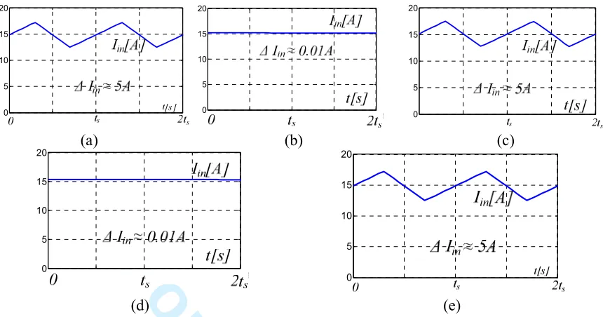
2. Dc input current ripple (∆Iin)
For energy conversion applications like PV, fuel cells, etc., current and voltage ripple cause harmonics and power loss in the overall system, so should be reduced. Ref [35] demonstrates that input current and voltage ripple inversely affect the total power extracted from PV systems. The simulation in Fig.4 shows the input current ripple for the three-phase buck-boost DM-CSIs at the circuit conditions in
TABLE I and Io = 10A. Generally, C5, G5 and D2 based DM-CSIs have the same input
current ripple versus input and output voltage. As an important feature, both D1 and F5 have insignificant input current ripple compared with the other inverters.
Vin(V)
Io(A) 5
10 15
20
0 100 200
3000
1 2 3 4
S1,S3,S5 D1,D3,D5 S2,S4,S6 D2,D4,D6
Io(A)
Vin(V)
5 10
15 20
50 100 150 200 250 300
0 2 4 6 8 10
C5 and G5 D1 and F5 D2
5 10 15 20 50
100 150
200 250
300 75
80 85 90 95 100
C5 and G5 D1 and F5 D2
E
ff
ic
ie
n
cy
(
%)
For Peer Review
(a) (b) (c)
[image:11.612.96.526.65.291.2](d) (e)
Fig.4. Matlab simulations of input current ripple of the five DM-CSIs: (a) C5, (b) D1, (c) D2, (d) F5, and (e) G5
TABLE I.PARASITIC COMPONENT VALUES AND CIRCUIT CONDITIONS
Parameter Value
Rated power 2.5 kW
Switching frequency fs = 50 kHz
Input inductor L1 = 1mH, r1 = 75 mΩ Output inductor L2 = 1mH, r2 = 75 mΩ
Input voltage Vin = 100 V
Output voltage Vm = 200 V
Output current angle γ = 0º
Diode forward voltage VDF = 2V
Switch on resistance Ron = 75mΩ
Transfer capacitor C = 10µF
Output capacitor Co = 2.5µF
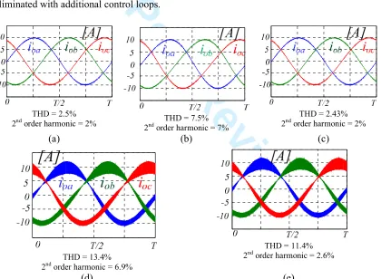
3. Output current THD
The output current distortion can be classified into low and high frequency distortion. Low order current distortion appears because of the non-linear nature and high system order of the proposed inverters and can be removed with appropriate control loops [24]. The high
0.028 0.028 0.028 0.028 0
5 10 15 20
0.028 0.028 0.028 0.028
0 5 10 15 20
0.028 0.028 0.028 0.028 0
5 10 15 20
0.128 0.128 0.128 0.128
0 5 10 15 20
0.028 0.028 0.028 0.028
0 5 10 15 20 2
For Peer Review
frequency current and voltage ripple in the output side occur because of the switching action. These high frequency ripple components are dependent on the converter topology which the differential-mode inverter descends from. The simulation in Fig.5 shows the output current and THD for the three-phase buck-boost DM-CSIs at the circuit conditions in
TABLE I when Io = 10A. From the simulation in Fig.5, C5, D1, and D2 have low THD
compared with F5 and G5 for the same passive element values. This is commensurate with the fact that these two inverters are descendent from power converters with discontinuous output current therefore, should have a higher output capacitance value Co. All inverters have
considerable negative-sequence second order harmonic current components which can be
eliminated with additional control loops.
THD = 2.5%
2nd order harmonic = 2% 2nd THD = 7.5%
order harmonic = 7%
THD = 2.43% 2nd order harmonic = 2%
(a) (b) (c)
THD = 13.4% 2nd order harmonic = 6.9%
THD = 11.4% 2nd order harmonic = 2.6%
[image:12.612.100.520.314.622.2](d) (e)
Fig.5. Matlab simulations of output current of the five DM-CSIs: (a) C5, (b) D1, (c) D2, (d) F5, and (e) G5
4. Capacitor voltage stresses
Knowledge of the voltage stresses on the energy transfer capacitor C is important for its specification. For some inverters, the voltage across C consists of a dc-bias plus a sinusoidal
-15 -10 -5 0 5 10 15
-15 -10 -5 0 5 10 15
For Peer Review
voltage component (fundamental) while for other converters, the voltage across C is only dc. Inverters using F5 and G5 have lower capacitor voltage stresses than C5, D1 and D2. TABLE
II summarizes the capacitor voltage stress for each converter, in terms of the source voltage and differential sinusoidal output maximum voltage, Vm.
TABLE IIVOLTAGE STRESS ACROSS CAPACITOR C(SEE FIG.2)
Topology Minimum dc-bias Sinusoidal voltage (fundamental) Peak Voltage
C5 Vin+Vm Vm sinωt Vin +2Vm
D1 Vin+Vm Vm sinωt Vin +2Vm
D2 Vin+Vm Vm sinωt Vin +2Vm
F5 Vin ≈0 Vin
G5 Vin ≈0
V
inIV. CONTROL STRATEGIES FOR THREE-PHASE BUCK-BOOST DM-CSIS
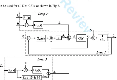
[image:13.612.104.523.185.324.2]The five three-phase buck-boost DM-CSIs under investigation are high order systems where classical control design is difficult and complex to implement. The small-signal transfer functions of the DM-CSIs are presented in Appendix A. A general control scheme can be used for all DM-CSIs, as shown in Fig.6.
Fig.6. Control scheme for buck-boost three-phase DM-CSIs.
[image:13.612.102.510.411.692.2]For Peer Review
(a) (b) (c)
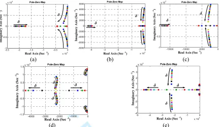
(d) (e)
Fig.7. Open loop poles loci of buck-boost three-phase DM-CSIs: (a) C5, (b) D1, (c) D2, (d) F5, and (e) G5.
The control scheme consists of three feedback loops:
1. Loop 1
[image:14.612.91.524.67.318.2]The first loop controls the fundamental components of the output current and voltage. The poles loci of the small-signal transfer functions G(s) for the different inverters are shown in Fig.7. To control the fundamental current (io), Gc1(s) is chosen as a PR controller:
1 1
( )
=
1+
2 2+
r c p oK s
s
K
G
s
ω
(8)The three degrees of freedom from the loop gains (Kp1, Kr1, and K) will be used to obtain fast
response, low current oscillation, and good stability margins. Taking inverter C5 as an example, the closed loop transfer function is expressed as:
1 1
( )
(1
)
=
+
+
c CL g cKG G
t
G
sL
KG
KG G
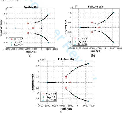
(9)Fig.8 plots the closed loop poles with variation of proportional gain value Kp1 with three
different values of K. The system is always stable for 0.5<Kp1<5. Consequently, Kp1= 2.5, in
the middle of the trajectory, is chosen for the experimentation. The main functions of the
Pole-Zero Map
Real Axis (seconds-1)
Im a g in a ry A x is ( s e c o n d s -1)
-2.5 -2 -1.5 -1 -0.5 0
x 104 -1
-0.5 0 0.5
1x 10 4 Im agin ar y Axis ( S ec -1)
-4 -3 -2 -1 0
x 104 -8000 -6000 -4000 -2000 0 2000 4000 6000
8000 Pole-Zero Map
Real Axis (seconds-1)
Im a g in a ry A x is ( s e c o n d s -1) Im agin ar y Axis ( S ec -1) Pole-Zero Map
Real Axis (seconds-1)
Im a g in a ry A x is ( s e c o n d s -1)
-15000 -10000 -5000 0 -1
-0.5 0 0.5
1x 10
4 Im a g in a ry A x is ( S ec -1) Pole-Zero Map
Real Axis (seconds-1)
Im a g in a ry A x is ( s e c o n d s -1)
-4000 -3000 -2000 -1000 0
-1.5 -1 -0.5 0 0.5 1 1.5x 10
4 Im ag in a r y A xi s (S ec -1) Pole-Zero Map
Real Axis (seconds-1)
Im a g in a ry A x is ( s e c o n d s -1)
-5 -4 -3 -2 -1 0
x 104 -4 -3 -2 -1 0 1 2 3 4x 10
4
δ δ
δ δ Im a g in a ry A x is ( S e c -1)
For Peer Review
inner loop gain K, are to increase the overall system bandwidth, and hence achieve fast response, as well as to damp resonance between the inverter inductors and capacitors. However, increased K leads to lower phase margin and hence, affects overall system stability. The value of K = 40 is selected to optimize the bandwidth and phase margin, see Fig.9. The resonant gain of the controller (Kr1) reduces the steady state error at the fundamental
frequency (ωo). Because of DM-CSI transfer function complexity, this gain is tuned during
simulation and experimentation. Kr1= 20 gives an acceptable steady state error and transient
response at ωo.
(a) (b)
[image:15.612.95.518.259.649.2](c)
Fig.8. Variation of Loop 1 closed loop poles with controller proportional gain Kp1. (a) K = 10,
Kr1 = 20, Kp1= 0.5→20, (b) K = 50, Kr1 = 20, Kp1= 0.5→20, and (c) K = 100, Kr1 = 20, Kp1=
0.5→20
Pole-Zero Map
Real Axis
Im
a
g
in
a
ry
A
x
is
-10000 -8000 -6000 -4000 -2000-2 0 2000 4000 -1.5
-1 -0.5 0 0.5 1 1.5
2x 10
4 Pole-Zero Map
Real Axis
Im
a
g
in
a
ry
A
x
is
-10000 -8000 -6000 -4000 -2000-2 0 2000 4000 -1.5
-1 -0.5 0 0.5 1 1.5
2x 10 4
Pole-Zero Map
Real Axis
Im
a
g
in
a
ry
A
x
is
-10000 -8000 -6000 -4000 -2000-2 0 2000 4000
-1.5 -1 -0.5 0 0.5 1 1.5
2x 10
4 2
For Peer Review
Fig. 9. Variation of Loop 1 frequency response with controller gain K values (Kp1 = 2.5, Kr1 = 20).
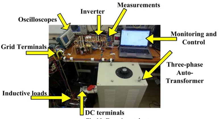
[image:16.612.92.479.474.684.2]Increasing K leads to better and faster inverter fault current limiting capability. However, there is a tradeoff between increasing K and having acceptable stability margins for Loop 1. The system concept, presented mathematical analysis, and simulations, are validated with a 2.5 kW DM-CSI as in Fig.1, with the parameters in TABLE I, controlled using a TMS320F280335 DSP. Fig.10 shows the experimental rig. Fig.11 shows DM-CSI operation with Loop 1, along with the resultant second order distortion.
Fig.10. Experimental setup.
-100 -50 0 50 100
M
a
g
n
it
u
d
e
(
d
B
)
101 102 103 104 105 106
-180 -90 0 90
P
h
a
s
e
(
d
e
g
)
Above : K = 40, Bandwidth = 2.85 kHz, phase margin = 95 deg Below : K = 10, Bandwidth = 830 Hz, phase margin = 128 deg
Frequency (Hz) 2
For Peer Review
2nd harmonic = 4% (Co = 2.5µF)5ms/div – 10A/div 2
nd
harmonic = 7% (Co = 2.5µF)
5ms/div – 10A/div 2
nd
harmonic = 3% (Co = 1µF)
5ms/div – 10A/div
(a) (b) (c)
Phase1: 2nd harmonic = 5% (Co = 15µF)
5ms/div – 10A/div
Phase1: 2nd harmonic = 3% (Co = 15µF)
5ms/div – 10A/div
(d) (e)
Fig.11. Operation of three-phase buck-boost DM-CSIs with Loop 1: (a) C5, (b) D1, (c) D2, (d) F5, and (e) G5.
2. Loop 2
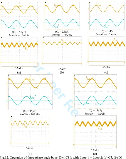
Control Loop 2 is necessary to eliminate the second order harmonic current in the output three-phase current because of the nonlinearity of the buck-boost DM-CSIs; see Fig.11. This nonlinearity can be sensed from the open loop pole loci of the inverters as the poles move through the long trajectory with different duty ratios. The second order harmonic current component increases with increase inverter passive element values. However, such an increase may be necessary for some applications when the switching frequency is to be lowered. The second order harmonic current is extracted with a band-pass filter F2(s) and fed
to a resonant controller Gc2(s) at double the fundamental frequency to calculate the required
second order duty ratio δ2. The filter gain (a2)is selected to adjust the filter’s bandwidth to
cater for a ±1% frequency variation.
For Peer Review
(Co = 2.5µF)5ms/div – 10A/div
3A/div
(Co = 2.5µF)
5ms/div – 10A/div
3A/div
(Co = 1µF)
5ms/div – 10A/div
3A/div
(a) (b) (c)
(Co = 15µF)
5ms/div – 10A/div
3A/div
(Co = 15µF)
5ms/div – 10A/div
3A/div
[image:18.612.95.524.62.603.2](d) (e)
Fig.12. Operation of three-phase buck-boost DM-CSIs with Loop 1 + Loop 2: (a) C5, (b) D1, (c) D2, (d) F5, and (e) G5
Unlike Loop 1, fast dynamics for Loop 2 is not pressing. Therefore, Kr2 is selected much
lower than Kr1in order not to conflict Loop 1 performance.
For Peer Review
2 2
2 2 2
( )
1
1
(4
)
=
+
+
π
a s
F s
s
a s
f
(10)
2 2
( )
2 24
=
+
r c
o
K s
s
G
s
ω
(11)Fig.12 shows the experimental operation of Loop 1 and Loop 2 when the second order output harmonic current component is suppressed to less than 1% in all five cases.
3. Loop 3
From Fig.12, all the DM-CSIs suffer from a third order oscillating current component in the input dc current. This comes from the fact that the input currents (iina, iinb, and iinc) all have
in-phase third order harmonic current components that sum up to the input dc current. As with the second order components in the three-phase output current, the third order component in the input dc current increases with higher passive elements values. If the third order current component in the input dc current Iin is expressed as:
3
( )
=
3sin(3
+
)
in in
i
t
I
ωt
λ
(12)then the oscillating power in the dc side is:
3in
( )
=
in in3( )
=
in in3sin(3
+
)
Q
t
V
i
t
V
I
ωt
λ
(13)Instead of oscillating in the input side, this oscillating power can be stored in the output capacitor Co. As shown in Fig.13, each Co has an additional third order harmonic voltage
component v3(t)=V3.sin(3ω+φ). Being co-phasal, the voltage v3(t) is not seen by the output
load.
For Peer Review
Fig.13. Elimination of the third harmonic current component in the input dc current Iin.
In order to supress Qin3, the total instantaneous power across the output capacitors is:
3out
( )
9
C
o m 3cos(3
)
3in( )
Q
t
=
ω
V V
ωt
+
φ
= −
Q
t
(14)Solving (13) and (14) yields:
in3 in 3
m o
3 2
V I
V
9ωV C
φ
λ
π
=
= −
(15)The feed-forward duty ratio δ3FF, shown in Fig. 6, can be calculated as: 3
3 FF
in 3
v ( t )
δ
V
v ( t )
=
+
(16)The function of the resonant controller Gc3(s) is to fix the small error arising from the
calculations in (15) and (16). Therefore, the gain Kr3 can be selected much lower than Kr1 in
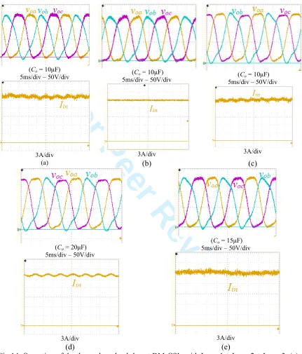
order not to interfere with the main loop. Fig.14 shows the experimental results when Loop 3
For Peer Review
is added to the control system, where the input current third order harmonic components of the five inverters are suppressed.
(Co = 10µF)
5ms/div – 50V/div
3A/div
(Co = 10µF)
5ms/div – 50V/div
3A/div
(Co = 10µF)
5ms/div – 50V/div
3A/div
(a) (b) (c)
(Co = 20µF)
5ms/div – 50V/div
3A/div
(Co = 15µF)
5ms/div – 50V/div
3A/div
[image:21.612.96.527.114.619.2](d) (e)
Fig.14. Operation of the three-phase buck-boost DM-CSIs with Loop 1 + Loop 2 + Loop 3: (a) C5, (b) D1, (c) D2, (d) F5, and (e) G5.
For Peer Review
V. INVERTER ISOLATIONFor reasons related to noise mitigation, electromagnetic compatibility and insulation, galvanic isolation between the input and output of the power converters is necessary in many applications [36]. Some of the proposed inverters can be modified to offer the possibility for transformer coupling and isolation. Generally, there are two main methods for power converters transformer coupling. In the first, a magnetic core temporarily stores the energy and then releases it to the output side [37]. However, the maximum transferred energy is limited by core volume as it equals ½BH×Volume. In the second method, the magnetic energy is transferred through instantaneous transformer action rather than being temporary stored in an intermediate magnetic circuit and then released. Thus, relatively small core volume can be used, where Faraday’s equation, v=Ndφ/dt, is applicable.
i. Considering the case of a typical G5 converter, the differences between the two methods is shown in Fig.15a. In Fig.15b, the energy is temporarily stored in the magnetic isolation transformer. Although the average voltage across the transformer is zero in G5 in Fig.15b, the transformer core is exposed to a dc bias current and flux because of the stored energy; thus, the core volume (for a given current ripple) is increased. Such dc current bias increases core power loss and decreases its maximum current utilization.
ii. The series energy transfer intermediate capacitor can be split into two and placed at both sides of the isolation the transformer as shown in Fig.15c. The energy transfer from the input to the output is achieved instantaneously, without energy storage in the transformer core.
With the two methods, the average voltage across the transformer is zero. If the turns ratio
N2/N1 is greater than 1, the converter voltage output Vo can be increased to offer a higher
voltage range. Of the known 33 single-switch single diode power converters in [34], seven converters, all buck-boost, can be isolated using a high frequency transformer (those with
For Peer Review
single element shunt paths and a shunt inductor [temporary storage action] and/or series capacitor[transformer action]), of which three have continuous input current, namely C5, F5, and G5; see TableIII.
(a)
(b) (c)
Fig.15. G5 converter: (a) non-isolated converter, (b) magnetic storage coupling, and (c) instantaneous transformer coupling.
TABLE III Transformer-isolated buck-boost converters with continuous input current
T
o
p
o
lo
g
y
C5 G5 F5
C
o
u
p
li
n
g
M
et
h
o
d
Instantaneous energy transfer
Instantaneous energy transfer
Temporarily stored energy
C
u
rr
e
n
t
b
ia
s
0 0 Iin
S
p
li
t-C
a
p
a
c
it
o
r
V
o
lt
a
g
es
Vc1 = Vin , Vc2 = Vo Vc1 = Vin , Vc2 = 0 -
The three buck-boost DM-CSIs having HFL isolated abilities are shown in Fig.16. Experimental comparison between the efficiencies of non-isolated and isolated versions of the three inverters is presented in Fig.17. The transformer core is a nano-crystalline material
L1
L2
Vc1
+
-Vin Vo
S1
D2
S2
D1
Iin
+
-Co
Z
Io
+
-V1
+
-V2
C
+
For Peer Review
which has high permeability (high magnetising inductance) and low leakage inductance. However, from Fig.4d, F5 has the preferable advantages of low input current ripple. But increased load current reduces the total inverter efficiency more than in C5 and G5 because of the core dc-bias current and average net core flux. The transformer action of C5 and G5 offers higher efficiencies than with the energy storage action of F5.
(a)
(b)
(c)
Fig.16. HFL isolated three-phase buck-boost DM-CSIs: (a) C5, (b) G5, and (c) F5.
r1 L1 r2 L2 S1 + + voa -Co Cp vga iina ioa Iin Vin
D1 i
L2a D2 S2 . r1 L1 r2 L2 + +v ob -Co Cp vgb iinb iob
D3 i
L2b D4 S4 . S3 r1 L1 r2 L2 + +v ob -Co Cp vgc iinc ioc
D5 i
L2c D6
S6
. S5
Lg Lg Lg
Cs +
G2
+Cs
G2 G2
+Cs
r1
L1
C
vca Co
iina Iin Vin D1 +
-S1 r2
L2 . voa + -S1 D2 r1 L1
C Co
iinb
D3
+
-S3 r2
L2 . vob + -S4 D4 r1 L1
C Co
iinc
D3
+
-S3 r2
L2 . voc + -S4 D4
vcb vcc
vga vgb vgc
iL2a iL2b iL2c
ioa iob ioc
Lg
Lg
Lg
G2 G2 G2
For Peer Review
(a) (b)
(c)
Fig.17. Experimental efficiencies of isolated and non-isolated versions of buck-boost three-phase DM-CSIs: (a) C5, (b) G5, and (c) F5.
VI. CONCLUSION
The paper investigated three-phase buck-boost inverters based on three differentially-connected reversible converters which have advantages when embedded in renewable energy generation systems. The presented DM-CSIs provide a flexible output voltages range as well as continuous input currents. This means the total dc side ripple current is low, (without recourse to electrolytic capacitor filtering), which is an important feature for MPPT techniques used in renewable energy systems.
A comparison between the DM-CSIs highlighted their main differences. The C5 and G5 based inverters have the lowest power loss and hence the best efficiencies. However, they experience higher input current ripple and may require higher input inductor values. Converters D1 and F5 have good efficiency at higher input dc voltages while the efficiency deteriorates at lower input voltages. The efficiency of D2 is lower than D1 and F5 at high input voltage and is better when the input voltage is lowered. In terms of device rating, the all
Series1
Series2
Series1
Series2
Series1
Series2
250 500 750 1000 1250 1500 1750 2000 2250 2500
87 88 90
Isolated Version Non-Isolated
Version
Output Power (W) 89
For Peer Review
five inverters topologies have the same performance. Using the same passive element values, D2 inverter is found to have the lowest THD in the output voltage and current waveforms. D1 and F5 inverters have very low input ripple current, which is an attractive feature for PV systems. F5 and G5 inverters have the lowest capacitor voltage stresses and hence smaller and cheaper capacitors can be used.
The main challenge of DM-CSI implementation is that they are non-linear converters where the dynamics depend on the operation point and duty ratio. This high order transfer function hampers easy classical control design. Accordingly, the inverters investigated suffer from negative sequence second order harmonic in the output current, which affect the output current THD and hence, require larger output filters, and third order harmonic in the total input dc side current, which affects the MPPT techniques of the input sources.
Three control loops to control the fundamental currents and voltages and to remove the mentioned input and output currents distortion were implemented. The control design can effectively improve the operation and response of the different DM-CSIs. Finally, high-frequency transformer isolation methods for three-phase buck-boost DM-CSIs were investigated. In the first method, the inverter is isolated by small-size cores and the energy is transferred between the input and output sides instantaneously by transformer action. In the second method, part of the energy is temporarily stored in the coupling circuit core which requires larger cores. The generated topologies and their operation as isolated inverters were illustrated. Comparison between the efficiency of the isolated and non-isolated versions showed the coupled version suffers higher core losses which decrease efficiency.
For Peer Review
APPENDIXA.1 Power loss in the semiconductor devices
The rated power of the inverters investigated is 2.5 kW. For all three-phase buck-boost DM-CSIs, the current through devices S1-D1 (which is the same for S3-D3 and S5-D5), is
shown in Fig.A1.
Fig.A1. Devices S1-D1current.
The envelope of the switch current can be expressed as:
1
1
( )
1
=
−
inv o
a
t
i
i
δ
(A.1)The rms value of the switch current is1 is:
( )
2( )
/2 /2 2 2
1( ) 1 1
0 0
1
1
.
.
.
T T
s rms s env a
I
i
dt
i
δ dt
T
T
=
∫
=
∫
(A.2)sin
sin
dc m
a
dc m in
V
V
ωt
δ
V
V
ωt V
+
=
+
+
(A.3)2
2 2 2
1( )
2 1 1 2 2
16 8
{
(¼
0.1061
(cos
1)) 0.2122
(cos
1)
(
cos ) ¼
o
s rms in dc m m dc
in
m dc
I
I
V
V
V
γ
V V
γ
V
V
γ
V
=
+
+
+
+
+
+
+
(A.4)
i
S1i
D1t
Device
current
i
env10 T/2 T
For Peer Review
If the inverter operates at unity power factor (γ = 0º) and Vdc = Vm, then (A.4) yields:
2 2
1( ) 2
(0.4622
0.8619
)
m o in m
s rms
in
V I
V
V
I
V
+
=
(A.5)The average value of the diode current iD1 is calculated from:
( )
( )
1 1 1
/2 /2 /2
1
1
1
.
1
(4
)
4
T T T
a
D D inv o
T T T a
m o
in
δ
I
i
dt
i
dt
i
dt
T
T
T
δ
V I
π
πV
=
∫
=
∫
=
∫
−
−
=
(A.6)
The power loss in device S1-D1 can be approximated as:
2
1 1( ) 1
device on s rms D DF
P
=
R
I
+
I
V
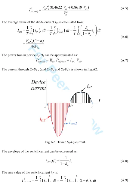
(A.7) [image:28.612.88.550.93.697.2]The current through S2-D2 , (and S4-D4 and S6-D6), is shown in Fig.A2.
Fig.A2. Device S2-D2current.
The envelope of the switch current can be expressed as:
2
1
( )
1
−
=
−
inv o
a
t
i
i
δ
(A.8)The rms value of the switch current is1 is:
( )
2( )
22
1( ) 2 2 /2 /2
1
1
.
. (1
).
T T
s rms s env a
T T
I
i
dt
i
δ
dt
T
T
=
∫
=
∫
−
(A.9)For Peer Review
22 2
2( )
1
cos
[
(0.0266 cos2
0.0796
)]
4
2
dc
in m
s rms o
in
V
V
V
γ
I
I
γ
V
π
+
=
+
−
−
(A.10)If the inverter operates at unity power factor (γ = 0º) and Vdc = Vm, then (A.10) yields:
2 2
2( )
0.0378
(¼
m)
s rms o
in
V
I
I
V
=
+
(A.11)The average value of the diode current iD1is calculated from:
( )
( )
( )
/2 /2 /2
2 2 2
0 0 0
1
1
1
.
T T T
D D inv o
o
I
i
dt
i
dt
i
dt
T
T
T
I
π
=
∫
=
∫
=
∫
=
(A.12)
The power loss in the S2-D2 can be approximated as:
2
2 2( ) 2
device on s rms D DF
P
=
R
I
+
I
V
(A.13)A.2 Power loss in the inductors
The currents through inductors L1 and L2 can be expressed as functions of the output current,
voltage and duty ratio, as shown in TABLE A.1. The quantity 1
1−δ is always greater than 1 while
1
δ
δ
− is greater than 1 when δ > 0.5 and less than 1 when δ < 0.5. 2
For Peer Review
TABLE A.1 CONVERTER INDUCTOR CURRENTSTopology Current through L1
iL1
Current through L2
iL2
C5
1 io iin
δ
δ =
−
i
oD1
1 io iin
δ
δ =
−
1 1−δ io
D2 1
1
in o
i
i δ
δ =
−
o
i
F5
1 io iin
δ
δ =
−
1 1−δ io
G5
1 io iin
δ
δ =
−
i
oFor the first phase, as an example, the quantities 1
δ δ
− a
o a
i and 1
1−δaiocan be expressed as:
( ) sin cos 2
1 2 2
a m o m o m o
o
a in in in
V I V I V I
i t t t
V V V
δ
ω ω
δ = + −
− (A.14)
1
( ) (1 ) sin cos 2
1 2 2
m o m m o
o o
a in in in
V I V V I
i t I t t
V V ω V ω
δ = + + −
− (A.15)
Then the copper losses of the different DM-CSIs are listed in TABLE A.2.
TABLE A.2COPPER LOSSES Type
Copper losses / r
L1 L2
C5 7ܸ
ଶܫ ଶ
8ܸଶ
½ܫଶ
D1 7ܸ
ଶܫ ଶ
8ܸଶ
ܫଶ[൬8ܸ7ܸ
+ 1൰ + ½]
D2 ܫଶ[൬7ܸ
8ܸ+ 1൰ + ½] ½ܫ
ଶ
F5 7ܸ
ଶܫ ଶ
8ܸଶ ܫ
ଶ[൬7ܸ
8ܸ+ 1൰ + ½]
G5 7ܸ
ଶܫ ଶ
8ܸଶ ½ܫ
ଶ
For Peer Review
A.3 Input current ripple
The input ripple current of the DM-CSIs are listed in TABLE A.3 TABLE A.3INPUT CURRENT RIPPLE
Topology p-p
C5 2.88ܸܸݐ௦
ܮଵ(1.44ܸ+ ܸ)
D1 0.72ܸܸܫݐ௦
ଶ
ܮଵܥ(1.44ܸ+ܸ)ଶ
D2 2.88ܸܸݐ௦
ܮଵ(1.44ܸ+ ܸ)
F5 0.72ܸܸܫݐ௦ଶ
ܮଵܥ(1.44ܸ+ܸ)ଶ
G5 2.88ܸܸݐ௦
ܮଵ(1.44ܸ+ ܸ)
A.4 Transfer function G(s)
(a) C5
2
o 2 1 0
3 2
3 2 1 0
2 e 1 in
2
1 in 1 e 1 e
2 2
0 in e e 1
2
3 1 2 e
2 2 2
2 1 2 e 2 e 2 e 2 1 e
2 3 4 2
1 1 e e e 2 e e
V ( s ) a s a s a G( s )
( s ) b s b s b s b a CR( 1 D )L V
a V ( L D CRr ( 1 D )) a V ( R( 1 D ) D r ) b CL L ( 1 D )
b CL ( R r D r 2 D ( R r ) D R ) CL r ( 1 D )
b L ( D 2 D D ) L ( 1 6 D 4 D
δ
+ +
= =
+ + +
= −
= − + −
= − −
= −
= + + − + + + −
= − + + + −
%
3 4
e e
2 2
1 e 1 2 e e 1 2
4 2 2 4
0 e 1 e e 2 e
D 4 D )
CRr ( 1 D ) C r r ( 1 D ) 2CD r ( R r ) b R( 1 D ) r D ( 1 D ) r ( 1 D )
+ −
+ + + + − +
= − + − + −
(A.16)
For Peer Review
(b)D1
2
o 2 1 0
3 2
3 2 1 0
2 e 1 in
1 in e 2 1 e 1 e
2
0 in e e in 2 1 e
2
3 1 2 e
2
2 e 1 2 2 1
2 2
1 e 2 1 e 1 2 1
V ( s ) a s a s a G ( s )
( s ) b s b s b s b a C R( 1 D )L V
a V ( D ( L L D ) C Rr ( 1 D )) a RV ( 1 D ) D V ( r r D ) b C L L ( 1 D )
b C ( 1 D ) [ L ( R r ) L ( R r )] b ( 1 D ) [( L L D ) C R( r r ) C r
δ + + = = + + + = − = − + + − = − − − + = − = − + + + = − + + + + % 2
2 2 2
0 e e 2 1 e
r ] b =( 1−D ) [ R( 1−D ) +( r +r D )]
(A.17)
(c) D2
o 1 0
3 2
3 2 1 0
1 e in 1 2
0 in e 1 e
2
3 1 2 e
2
2 e 1 2 2 1
2 2
1 e 1 2 e 1 2 1
2 2
0 e 2 e 1
V ( s ) a s a
G ( s )
( s ) b s b s b s b
a D V L
a V [ R ( 1 D ) r D ]
b CL L ( 1 D )
b C ( 1 D ) [ L ( R r ) L r ]
b ( 1 D ) [ L L ( 1 D ) Cr r CR r ]
b ( 1 D ) [( R r )( 1 D ) r ]
δ + = = + + + = − = − − = − = − + + = − + − + + = − + − + % (A.18) (d)F5 3 2
o 3 2 1 0
3 2
3 2 1 0
2 3 e 1 2 in
2 e in 1 2 2 1 1 e
2
1 in e 1 e 1 1 2 2 2 1 e
2
0 in e e e 1 2
2 2
4 o 1 2 e
2
3 1 e 1
V ( s ) a s a s a s a
G ( s )
( s ) b s b s b s b
a C D L L V
a C D V [( L r L r ) L R( 2 D )]
a V [ D L ( D L Cr r L ) CL Rr ( 1 D ) ]
a V [ R( 1 D ) D ( D r r )]
b C C L L R( 1 D )
b CL ( 1 D ) [ L
δ + + + = = + + + = = − + + − = − + + − − = − − + = − = − %
2 o 1 2 2 1
2 2 2
2 1 e 1 e 1 2 2 1 o 2 e 1 2
2 2 2 2
1 1 e 2 e 1 1 e o 1 e 2
2 2 2
0 e e 2 1 e
L C R( L r L r )]
b L ( 1 D ) [ CL R( 1 D ) C ( L r L r ) C ( L R D CRr r )]
b L ( 1 D ) [ L D L CRr ( 1 D ) C R( r D r )]
b ( 1 D ) [ R( 1 D ) r r D ]
For Peer Review
(e) G5
3 2
o 3 2 1 0
3 2
3 2 1 0
3 e 1 2 in 2
2 in e 1 2
2 2
1 in e 1 2 e in 1 2 e 1 in
2 2
0 in e e in 1
2
4 o 1 2 e
2 2
3 1 2 e o e 1 2
V ( s ) a s a s a s a
G ( s )
( s ) b s b s b s b
a CD L L V
a CRV ( 1 D ) ( L L )
a C RV ( 1 D ) ( r r ) C D V r r D L V
a RV ( 1 D ) D V r
b CC L L R( 1 D )
b CL L ( 1 D ) CC R( 1 D ) [ r L
δ
+ + +
= =
+ + +
= −
= − +
= − + − −
= − −
= −
= − + − +
%
2 1
4 4 2 2
2 e 1 2 o 2 e o 1 e e
2 2
e 1 2 2 1 o 1 2 e
4 2 2
1 2 e 1 e e 1 2
2 2 4 2
o e e 1 e 1 2 1 2 e
4 2
0 e 2 1 e
r L ]
b CR( 1 D ) ( L L ) C L R( 1 D ) C L RD ( 1 D )
C ( 1 D ) ( L r L r ) CC Rr r ( 1 D )
b L ( 1 D ) L D ( 1 D ) CR( r r )
C ( 1 D ) [( 1 D ) Rr ] CR( 1 D ) [ r r ] Cr r ( 1 D )
b ( 1 D ) ( R r ) r D (
= − + + − + −
+ − + + −
= − + − + + +
− − + + − + + −
= − + + 2
e
1−D )
(A.20)