ePrints Soton
Copyright © and Moral Rights for this thesis are retained by the author and/or other copyright owners. A copy can be downloaded for personal non-commercial
research or study, without prior permission or charge. This thesis cannot be
reproduced or quoted extensively from without first obtaining permission in writing from the copyright holder/s. The content must not be changed in any way or sold commercially in any format or medium without the formal permission of the
copyright holders.
When referring to this work, full bibliographic details including the author, title, awarding institution and date of the thesis must be given e.g.
)$87<2)(1,1((5,16,(1(0$7+(0$7,6
2372((7521,65(6($5+(175(
89
!
6
""#
,
/
$"%
1
&'
'(
/
$"%
7
'')'
E*
,
'))
KHVLVIRUWKHGHJUHHRI'RFWRURIKLORVR+K*
ABSTRACT
FACULTY OF ENGINEERING, SCIENCE AND MATHEMATICS OPTOELECTRONICS RESEARCH CENTRE
Doctor of Philosophy
Direct UV Writing of Structures in Lithium Niobate and Lithium Tantalate By Iain Wellington
This thesis presents results from fabrication of UV direct write structures in lithium niobate and lithium tantalate. Unassisted direct writing of surface channel waveguides using Ȝ = 244 nm cw light resulted in polarisation specific waveguides fabricated on z- cut crystals. Waveguides were characterised using mode profiles, propagation losses, numerical aperture and refractive index measurements. In z-cut congruent lithium niobate, waveguides were written on the +z and -z faces producing structures that guided TM polarisation only with +z face waveguides exhibiting the lowest propagation loss of ~ 2 dB/cm, a maximum refractive index difference of ~ 8 x 10⁻⁴ and a mean lifetime of IJ ~ 4.5 days. The waveguiding mechanism is believed to be due to a lithium out-diffusion enhanced by a transient photorefractive effect. Waveguides were also written in stoichiometric and doped samples to test improvements in waveguide lifetimes. Surface domain reversal was observed in congruent lithium niobate on both +z and –z faces. Channel waveguides written into lithium tantalate were characterised and compared with lithium niobate.
I, Iain Tristan Wellington declare that the thesis entitled Direct UV Writing of Structures in Lithium Niobate and Lithium Tantalate and the work presented in the thesis are both my own, and have been generated by me as the result of my
own original research. I confirm that:
this work was done wholly or mainly while in candidature for a research degree at this University;
where any part of this thesis has previously been submitted for a degree or any other qualification at this University or any other institution, this has been
clearly stated;
where I have consulted the published work of others, this is always clearly attributed;
where I have quoted from the work of others, the source is always given. With the exception of such quotations, this thesis is entirely my own work;
I have acknowledged all main sources of help;
where the thesis is based on work done by myself jointly with others, I have made clear exactly what was done by others and what I have contributed
myself;
parts of this work have been published as listed in Appendix A.
Signed: Iain Wellington………..
INTRODUCTION ... 6
1.1 Integrated Optics... 6
1.2 Synopsis... 8
1.3 References ... 10
LITHIUM NIOBATE ... 11
2.1 Introduction ... 12
2.2 Crystal Structure & Properties... 12
2.3 Optical Properties ... 17
2.3.1 Optical Transmission... 17
2.3.2 Birefringence ... 17
2.3.3 Electro-optic Effect ... 19
2.3.4 Pyroelectric Effect ... 20
2.3.5 Photovoltaic Effect ... 21
2.3.6 Photorefractive Effect... 21
2.4 Second Harmonic Generation ... 23
2.4.2 Phase Matching ... 25
2.4.3 Periodically Poled Crystals... 28
2.5 Conclusion... 29
2.6 References ... 30
2.6 References ... 30
WAVEGUIDE THEORY AND FABRICATION IN LINBO3... 34
3.1 Waveguide Theory ... 35
3.1.1 Introduction ... 35
3.1.2 Maxwell’s Equations ... 37
3.1.3 Dispersion Equations... 39
3.2 Waveguide Fabrication... 43
3.2.1 Introduction ... 43
3.2.2 Ion diffusion ... 43
4.1 Introduction ... 55
4.1.1 Ge:Doped Silica ... 56
4.1.2 Other Materials... 56
4.1.3 Lithium Niobate ... 57
4.2 The Writing System ... 57
4.3 Single Mode Waveguides at Ȝ = 633 nm ... 59
4.4 Single Mode Waveguides at Ȝ = 1549 nm ... 61
4.4.1 Physical Characteristics... 61
4.4.2 Optical Characteristics... 63
4.4.3 TE/TM ... 65
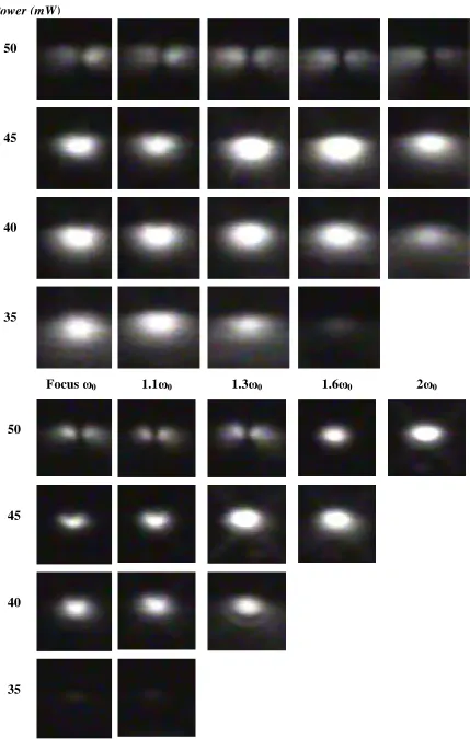
4.4.4 Mode profiles ... 66
4.4.5 Numerical aperture ... 69
4.4.6 Propagation Losses ... 70
4.4.7 Waveguide Stability ... 73
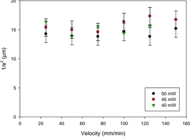
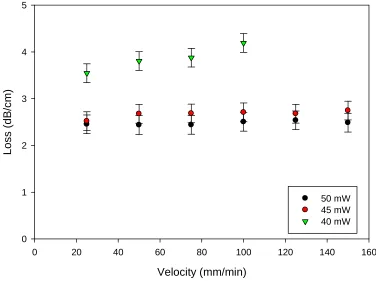
4.4.8 Variation of Writing Velocity... 76
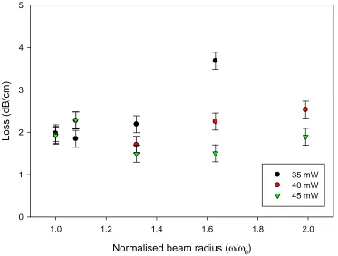
4.4.9 Variation of the Waveguide Width... 77
4.4.10 Multiple Passes... 80
4.5 S –Bends ... 84
4.5.1 Variation of Bend Length ... 85
4.5.2 Variation of Bend Offset ... 86
4.6 Y- Junctions ... 87
4.6.1 Variation of Arm Separation ... 88
4.7 UV Induced Index Changes in LiNbO3... 89
4.8 Possible Domain Formation ... 93
4.10 References ... 97
UV DIRECT WRITING IN STOICHIOMETRIC LINBO3, DOPED LINBO3 AND LITAO3... 103
5.1 Introduction ... 104
5.2 Stoichiometric LiNbO3... 105
5.3.1 Introduction ... 109
5.3.2 MgO:LiNbO3... 110
5.3.3 Zn:LiNbO3... 110
5.3.4 Fe:LiNbO3... 115
5.3.5 Er:LiNbO3 & Nd:LiNbO3... 120
5.4 Titanium in-diffused LiNbO3... 121
5.4 Waveguides in LiTaO3... 123
5.4.1 Introduction ... 123
UV PULSED DIRECT WRITING IN LINBO3... 132
6.1 Introduction ... 133
6.2 Experimental Procedure... 134
6.3 Results and Discussion ... 136
6.3.1 Z-cut exposures ... 136
6.3.2 Effect of Sample Rotation ... 143
6.3.3 Elevated Temperature Exposures ... 145
6.3.4 Exposures on Other Samples ... 146
6.3.5 Analysis and Discussion... 147
6.4 Mechanism of Poling ... 149
6.5 Summary ... 153
6.6 References ... 154
TEMPERATURE MODELLING OF UV HEATING OF LINBO3... 158
7.1 Introduction ... 159
7.2 Definition of Numerical Model... 161
7.2 UV cw Heating... 168
7.2.1 Beam Power ... 169
7.2.2 Beam Velocity ... 170
7.2.3 Temperature Related Effects ... 170
7.2.3.1 Crystal Stress ... 171
7.2.3.2 Pyroelectric Field... 174
7.3 UV Pulsed Heating ... 176
7.3.1 Fluence effects... 178
7.3.2 Multi-pulse regime ... 181
7.3.3 Melt depth vs. fluence ... 181
7.3.4 Temp increase vs. fluence ... 183
7.3.5 Stress and Pyroelectric Field ... 184
7.4 Numerical Model Future Work ... 185
7.5 Conclusion... 186
8.2 References ... 196
LIST OF PUBLICATIONS ... 197
Journal Papers... 197
Chapter 1
Introduction
1.1 Integrated Optics
Integrated optics today dominates the telecommunications industry with light sources used to transmit signals, optical fibres used to carry these signals and other devices, such as amplifiers used to manipulate or boost these signals.
photolithography techniques and semiconductor devices, the integrated optics field grew tremendously.
Two major breakthroughs galvanised the optical telecommunications industry. The first was the invention of semiconductor light sources, whether lasers for long distance communication or light emitting diodes for short distance communications, allow compact, cheap devices to be used. The second, optical fibre with low propagation loss, currently around 0.2dB/km, was important for long distance transmission of signals without signal loss and for high bandwidth applications. Suitable connectors are needed to ensure the signal is delivered into and out of the fibre with little degradation to the quality of the signal. Optical fibres can be used to amplify the signal by doping a fibre with an optically active element such as erbium. Amplification is achieved by stimulating emission from photons from the dopant ions. Although amplification is a useful process, many other manipulations of the signal are needed for an optical network. Planar devices fit this category and can be used for splitters, switches, modulators, interferometers and polarisers.
The important improvement with integrated optics is the optical confinement nature of all devices, allowing manipulation of light while on the substrate. Planar waveguide devices confine light in one dimension and are used to manipulate light in ways that fibre cannot. A sub-section of planar waveguides are channel waveguides in which light is confined in two dimensions and more complex devices can be realised with channel waveguides are they designed to used the single-mode of the signal. Devices that change the waveguide direction (interconnects), divide the signal (splitters), change the signal intensity/phase (modulators) and frequency converters (optical parametric oscillators) are fabricated in planar substrates because the size of the device can be made much smaller or the properties of the materials used can be exploited.
properties as identified by Ashkin in the mid-1960s [1]. Glasses, due to their amorphous structure, can be used as passive waveguides and, when doped with an active ion, waveguide lasers[2]. The use of silicon leads to the considerable desire of exploiting current fabrication methods and processes already in use in the electronics industry for the optics industry – the sheer scale of reduction of production costs is hugely compelling.
Ultraviolet direct writing in lithium niobate was initiated by Mailis, who had observed an index change on the surface of lithium niobate after exposure to 244nm light [3]. The direct writing technique had already been used successfully to produce waveguides and more complex devices such as gratings in germanium-doped silica [4], waveguides and waveguide lasers in chalcogenide glasses [5] and waveguides in a variety of other glasses as expanded on in chapter 4.
1.2 Synopsis
The motivation for this thesis is to investigate the relatively simple UV direct writing technique to fabricate integrated optics using lithium niobate as a substrate material. The second chapter introduces lithium niobate as a material and outlines its various properties relevant to this thesis, ranging from electro-optic to thermal properties. The third chapter will begin with a brief summary of the theory of waveguiding and how light propagates in optical devices; the chapter will then describe how lithium niobate has been used to produce integrated optics and will present a brief summary of the current state of the art fabrication techniques and some devices that have been realised.
1.3 References
1. Ashkin, A., G.D. Boyd, J.M. Dziedzic, R.G. Smith, A.A. Ballman, J.J. Levinstein, and K. Nassau, Optically-Induced Refractive Index Inhomogenities In LiNbO3
AND LiTaO3. Applied Physics Letters, 1966. 9(1): p. 72-74.
2. Guilhot, D.A., G.D. Emmerson, C.B.E. Gawith, S.P. Watts, D.P. Shepherd, R.B. Williams, and P.G.R. Smith, Single-mode direct-ultraviolet-written channel waveguide laser in neodymium-doped silica on silicon. Optics Letters, 2004.
29(9): p. 947-949.
3. Mailis, S., C. Riziotis, P.G.R. Smith, J.G. Scott, and R.W. Eason, Continuous wave ultraviolet radiation induced frustration of etching in lithium niobate single crystals. Applied Surface Science, 2003. 206(1-4): p. 46-52.
4. Emmerson, G.D., S.P. Watts, C.B.E. Gawith, V. Albanis, M. Ibsen, R.B. Williams, and P.G.R. Smith, Fabrication of directly UV-written channel waveguides with simultaneously defined integral Bragg gratings. Electronics Letters, 2002. 38(24): p. 1531-1532.
Chapter 2
Lithium Niobate
2.1 Introduction
Lithium niobate (LN, LiNbO3) is an artificial dielectric crystal, first fabricated in Bell Laboratories in the mid-sixties, and has various attractive properties which have been exploited in many applications. It is most commonly available in 3-inch diameter wafer and bulk crystal form and is inert at room temperature.
LiNbO3 is referred to as a non-linear crystal, but due to its ferroelectric properties, it possesses a wide range of both linear and non-linear properties, which are mentioned later and include the electro-optic effect, acousto-optic effect, photovoltaic effect, photorefractive effect, piezoelectric and pyroelectric effects. It has large non-linear coefficients, which make the material attractive for photonic applications such as harmonic conversion.
In this introduction, only the properties and effects that affect the UV writing experiments are mentioned. Weis and Gaylord have summarised all properties in a comprehensive review [1]. Section 2.2 covers the growth and structure of the crystal, section 2.3 discusses various optical properties of lithium niobate and section 2.4 outlines the basic process and use of lithium niobate in second harmonic generation.
2.2 Crystal Structure & Properties
Lithium niobate is usually manufactured using the Czochralski growth method [1]. It is commercially available in two main crystal compositions: congruent and stoichiometric. The composition is usually represented by a lithium ion concentration as given by:
Where the [ ] symbols denote concentrations. Congruent crystals have a lithium ion content of less than 50 %mol Li2O (typically ~48.5 mol% Li2O) while stoichiometric crystals have a lithium ion content much nearer to the ideal 50 mol% Li2O, and therefore congruent crystals are said to be lithium deficient compared to stoichiometric crystals. The exact composition of the crystal can also be estimated by measurements of the birefringence and the Curie temperature [2].
The Czochralski method uses a seed crystal which is dipped into a melt of congruent Li2O-Nb2O5 just above the melting temperature and is subsequently slowly rotated and raised. The composition of the crystal can be variable if produced in a non-congruent melt due to thermal effects from melt convection and lack of melt depth. For these reasons, some stoichiometric crystals are grown via a double crucible Czochralski method [3] and this allows a constant melt source to be continuously added thus allowing stoichiometric crystals of uniform homogeneity to be produced. Single crystal stoichiometric LN can also be produced via the single Czochralski process with the addition of 8 mol% K2O to the melt [4].
Figure 2.1: Crystallographic directions for ferroelectric lithium niobate [1].
as a result of elastic forces within the crystal lattice. The spontaneous polarisation is randomly aligned in one of two directions, either along the +c or – c direction. It can be made to align in a chosen direction along the c axis by the application of an external electric field while cooling through the Curie temperature. The Curie temperature of a material is a transition point above which the material exhibits no spontaneous polarisation as it has undergone a phase change, to the paraelectric phase and it has a different structure which is centrosymmetric – i.e. no spontaneous polarisation present.
Figure 2.2: Structure of LiNbO3 showing both paraelectric and ferroelectric phases [5].
The niobium and lithium ions are distributed between planes of oxygen atoms. Figure 2.2 illustrates the structure of the crystal in both the paraelectric and ferroelectric phases with the oxygen planes denoted as dashed lines for simplicity. The centre diagram is the paraelectric phase which has a net polarisation of zero due to the inversion symmetry of the crystal structure. Either side of the paraelectric phase is a diagram of the ferroelectric phase with the net polarisation aligned either along the +c or –c axis.
Ferroelectric Ferroelectric Paraelectric
Nb5+
Li+
If we include the oxygen planes, the structure of LiNbO3 at room temperature in the ferroelectric phase is shown in fig. 2.3. It is composed of layers of distorted octahedrons along the c axis.
Figure 2.3: Structure of LiNbO3 at room temperature [1].
Several congruent crystal properties are listed in table 2.1:
Property Value
Density 4648 kg/m3
Crystal Structure 3m
Melting Point 1240ºC
Curie Point 1140ºC
Specific Heat 633 J/kg K Thermal Diffusivity 1.36 x 10⁻⁵ m2/s
Table 2.1: Properties of congruent LiNbO3
2.3 Optical Properties
2.3.1 Optical Transmission
Lithium niobate has a wide spectral region for use in photonic applications; it is optically transparent in the region Ȝ ~ 0.4 – 5.0µm and the ultraviolet absorption edge, which occurs at ~ 320 nm is shown in figure 2.4.
2.3.2 Birefringence
LiNbO3 is a negatively birefringent uniaxial crystal. A polarisation parallel to the optic axis sees an extraordinary refractive index (ne) and a polarisation perpendicular
to the optic axis sees an ordinary refractive index (no) and the optic axis for lithium
λ (nm)
100 200 300 400 500 600 700
Tr an s m is s ion ( % ) 0 20 40 60 80
Figure 2.4: Transmission spectrum of congruent lithium niobate.
Through the Sellmeier equation in Eq. 2.2 it is possible to predict the refractive indices at different wavelengths and crystal compositions [7]. Table 2.2 gives the parameters needed for the Sellmeier equation and figure 2.5 illustrates the change in index over wavelength for congruent and stoichiometric lithium niobate.
2 2 , 1 , 1 2 2 , 0 , 0 2 1 100 50 1 100 50 1 λ λ λ λ i i Li i i Li i A C A C n − − + − + + = (2.2)
Parameter ne no
A0,i 3.854 3.489
400 600 800 1000 1200 1400 1600 2.1 2.15 2.2 2.25 2.3 2.35 2.4 2.45 2.5 Wavelength (nm) R e fr acti v e Inde x CLN, n o SLN, n o CLN, ne SLN, n
e
Figure 2.5: Extra-ordinary and ordinary refractive indices for congruent (full lines) and stoichiometric (dashed lines) lithium niobate [7].
2.3.3 Electro-optic Effect
The linear electro-optic effect (also called the Pockels effect) in LiNbO3 occurs when the refractive index of the crystal is modified by the application of an electric field. The linear electro-optic effect has the relationship [8]:
E r n
n 3 ijk
2 1 − = Δ (2.3)
Where ǻn is the change in refractive index, rijk the relevant electro-optic tensor
coefficient, and E is the applied electric field. The electro-optic tensor rijk has
different values due the symmetry of the crystal. Equation (2.4) lists the rijk
coefficients in lithium niobate.
¸ ¸ ¸ ¸ ¸ ¸ ¸ ¸ ¹ · ¨ ¨ ¨ ¨ ¨ ¨ ¨ ¨ © § − − = 0 0 0 0 0 0 0 0 0 0 22 42 42 33 13 22 13 22 r r r r r r r r
rijk (2.4)
This effect is exploited for use in modulators, an example of which is a Pockels cell [9], [10]. The highest linear electro-optic coefficient for LiNbO3 is the r33 coefficient,
which has a value of 30.8pm/V. For comparison, quartz has an r41 coefficient of only
1.4 pm/V.
2.3.4 Pyroelectric Effect
The pyroelectric effect considers the change in spontaneous polarisation ǻP with a change in temperature ǻT with a tensor multiplication factor p3 [11]:
T p P Δ » » » ¼ º « « « ¬ ª = Δ 3 0 0 (2.5)
The constant p3 is -4x 10⁻⁵ C K-1 m2 and is due to movement of the Li and Nb ions in
2.3.5 Photovoltaic Effect
The photovoltaic effect in LiNbO3 is the dominant charge migration mechanism and is a photo-induced current which ionises impurities when the crystal is uniformly illuminated. A voltage can be observed between the z faces when the sample is illuminated. This effect is important when the crystal is used for photorefractive applications.
2.3.6 Photorefractive Effect
The photorefractive effect is found in LiNbO3 crystals due to its electro-optic and photovoltaic properties. Exposure to optically intense inhomogeneous visible light induces a reversible change in the refractive index of the medium [12] and the crystal is more susceptible to wavelengths shorter than Ȝ ~ 1 ȝm. This effect is generally agreed to be a combination of several mechanisms – incident high intensity light excites charge carriers (electrons for visible light) which are promoted from donor states to the conduction band and then become mobile and, through migration, get trapped at new sites such as an empty donor or acceptor. Regions of high intensity therefore lose electrons while regions of low intensity acquire surplus electrons. This alters local space-charge fields, modulating the refractive index via the linear electro-optic effect (Eq 2.3).
I(z)
ρ( )
z
Δ
n(z)
+
+
+
--
-E(z)
+
+
+
+
+
Figure 2.6: Photorefractive mechanism for lithium niobate with light intensity I top, the charge density ȡ below, the resulting electric field via Poisson’s equation and the change in refractive index ǻn at the bottom.
Early on in the material’s characterisation, this effect was deemed detrimental to waveguide fabrication [13] as power dissipates throughout propagation, limiting the use of waveguides in LiNbO3 to low optical powers or operation at wavelengths beyond 1µm.
The effect is generally accepted to be due to iron impurities in the crystal [14] – iron
− +
+ +h →Fe +e
Fe2 ν 3 (2.6)
+ +
+ +h →Fe +h
Fe3 ν 2 (2.7)
Stoichiometric LN has been shown to have a reduction in optical damage compared to congruent LN [15]. The effect can persist for times that can vary from minutes to tens of years following exposure to illumination. Although unfavourable for optical waveguides, this can be an advantageous effect if these index changes are made permanent resulting in optical storage [16]. Doping the crystal with Fe ions increases the sensitivity of the material to light and becomes useful in applications such as holographic recording [17].
The crystals are often doped with magnesium oxide during the growth process for greater resistance to optical damage due to the photorefractive effect [18]. Zinc is also a useful dopant for reduced photorefractive sensitivity and it behaves in a similar way to magnesium. Approximately 4-6 mol% drastically changes the optical properties [19]. Recently, low Hf doping of ~0.5 %mol has also shown a resistance to optical damage [20].
2.4 Second Harmonic Generation
The demand for applications using shorter wavelengths is growing and the lack of suitable lasing devices in the UV to near-visible region of the spectrum means second harmonic generation from a fundamental frequency to a wave of double frequency is a suitable technique to achieve this. One of the main applications for lithium niobate crystals lies in second harmonic frequency conversion devices.
The types of frequency generation are sum frequency generation (SFG) sometimes called up conversion, difference frequency generation (DFG) or mixing, and optical parametric generation (OPG). SFG involves mixing two frequencies Ȧ1 and Ȧ2
Ȧ3 and Ȧ2 and producing the difference frequency Ȧ1. OPG is a similar process to
SFG but in reverse; the processes are governed by the frequency/energy conservation equations:
SFG: ω1+ω2 =ω3 (2.8)
DFG: ω3−ω2 =ω1 (2.9)
OPG: ω3 =ω1+ω2 (2.10)
Where Ȧ3 > Ȧ2 > Ȧ1. Second harmonic generation (SHG) is a specific case of sum
frequency generation when Ȧ1 = Ȧ2. To understand SHG, we look at the polarisation
of a non-linear crystal while an electric field is propagating through it. The linear polarisation, P, of a crystal is described by the vacuum permittivity İ0, the
susceptibility tensor Ȥ and the incident electric field, E:
(
(1) (2) 2 (3) 3 ...)
0 + + +
= E E E
P ε χ χ χ (2.11)
The susceptibility tensor, χijk(2), is related to the non-linear tensor, dijk, by:
) 2 ( 2 1 ijk ijk
d = χ (2.12)
Where d can be reduced in the same manner as r via the crystal symmetry and is described by [21]:
¸ ¸ ¸ ¹ · ¨ ¨ ¨ © § − − = 0 0 0 0 0 0 0 0 0 0 33 31 31 15 22 22 22 15 d d d d d d d d
nature of lithium niobate, there is a non-zeroχijk(2) present, and second order effects are possible. If we substitute an electric field of the form E = E0cos(ωt) into (Eq. 2.11) the polarisation response becomes:
( )
t E( )
t DC E P E E P + + = + = ω χ ε ω χ ε χ ε χ ε 2 cos 2 1cos 0 (2) 02 0 ) 1 ( 0 2 ) 2 ( 0 ) 1 ( 0 (2.14)
The first term is a response at the fundamental frequency, the second term is the response at the second harmonic frequency, at double the fundamental frequency, and the third term is a resulting DC electric field. The fundamental and second harmonic waves propagate throughout the crystal and the second harmonic term has an intensity proportional to the fundamental intensity squared:
¸ ¹ · ¨ © §Δ ∝ 2 sin ) ( ) 2
( I2 2L2 c2 kL
I ω ω ω (2.15)
The second harmonic intensity thus increases quadratically over the interaction length L and is wavelength dependent with the term ǻk the wave vector mismatch. If ǻk is non-zero, the second harmonic intensity is modulated throughout the crystal, reducing the conversion efficiency hence phase matching (i.e. phase velocity matching) is needed. The SHG phase matching condition is Δk =k2ω −2kω =0.
2.4.2 Phase Matching
In order to maximise non-linear conversion efficiencies and obtain useful output intensities, with the phase matching condition described in equation (2.16), the phase relationship between the two waves needs to be zero:
0 2 2 − =
=
Where kȦ and k2Ȧ are the wavevectors of the fundamental and frequency doubled
waves. As the waves propagate through the medium, they become more mismatched and out of phase due to dispersion so a solution is required to preserve Δk =0. There are two main ways of achieving phase matching in lithium niobate for second harmonic generation: angle tuning with temperature tuning and quasi-phase matching.
Angle tuning uses the birefringence of the crystal to achieve the phase matching condition. The incident beam has a specific polarisation and the crystal axes are orientated in a certain direction. The change in refractive index is obtained via varying the angle ș by:
( )
22
2 2
2
cos sin
1
o
e n
n n
θ θ
θ = + (2.17)
There are a few constraints with this method due to factors such as the small range of angles available, the Poynting-vector walk-off due to the difference in phase velocity and power flow directions (which restricts the interaction length) and use of alternative non-linear coefficients due to wave polarisation. Temperature tuning with angle tuning can be achieved via birefringence; the refractive indices are, and hence birefringence is, temperature-dependent and heating a correctly orientated crystal with a specific polarised incident beam fulfils the phase-matching condition.
the wave and increasing the second harmonic power once again. If the phase matching condition is not satisfied the second harmonic power reverts to zero after two coherence lengths. The QPM phase-matching condition has an extra grating vector term to account for the phase correction and is given by:
0 2 2
1 =
Λ − − =
Δk k k π (2.18)
Where the factor ȁ is the grating period and is 2Lc. Fig. 2.7 illustrates the second
harmonic intensity generated vs. interaction length for three conditions of phase matching: line a is perfect phase matching, line b quasi-phase matching with the inverted nonlinear coefficient every coherence length and line c the condition where no phase matching occurs.
Figure 2.7: Second harmonic generation intensity with a) perfect phase matching, b) quasi-phase matching and c) non-phase matched conversion. The coherence length is denoted as Lc.
that birefringent phase matching cannot [23]. Conversion efficiencies of 81% in zinc doped PPLN have been reported [24].
2.4.3 Periodically Poled Crystals
Originally, this process was envisaged by stacking thin sheets of material one coherence length in width in alternating directions, but practically this is extremely difficult as well as time-consuming. First realised in 1992, periodic domains were fabricated in lithium niobate via an external field at room temperature to produce devices for optical frequency generation [25]. The variety choice of period ȁ from Eq. 2.18 with the fundamental frequency allows a range of possible doubled frequencies for many non-linear applications. A constraint of this method is the period is limited by fabrication conditions, with periods of below 3 ȝm difficult with usual photolithographic techniques. For an example of parameters needed for a periodically poled crystal, the fundamental wavelengths of Ȝ = 915 nm and Ȝ = 1130 nm with crystal periods of 5.2 ȝm and 8.3 ȝm produce second harmonic efficiencies of ~ 24% and ~ 20% respectively in different samples [26].
Figure 2.8: PPLN second harmonic process.
Poling the crystal is typically achieved by patterning metal electrodes using photolithography, such as aluminium, on the +z face of the sample and applying a
Fundamental Fundamental
duration in order for the domain reversal to be permanent, Myers reported a time of between 0.36 - 1.9 seconds [28].
Lc
Lc
Conductive gel V
Crystal Top electrodes
-z +z
Figure 2.9: Apparatus used for periodic poling in +z cut lithium niobate. The spontaneous polarisation direction is denoted by blue arrows and reversed domains are dark grey.
Another method of electric field poling include spin coating a photoresist on the –z face instead of metal electrodes and patterning using a mask with photolithography. There are other techniques of poling without applying an external electric field which have been investigated such as heat treatment [29] but the methods generally lack the high degree of control over domain size and experimental practicality of electric field poling. More complex aperiodically poled lithium niobate can be used to produce several wavelengths at once via fabrication of a chirped grating [30].
2.5 Conclusion
Lithium niobate is a popular choice for integrated optics thanks to its high non-linear coefficients and ease of production. It is suitable for a wide range of applications including optical waveguiding, electro-optic modulators and frequency generation. As such, many commercial devices have been fabricated and lithium niobate is and will be the material of choice for the foreseeable future.
2.6 References
1. Weis, R.S. and T.K. Gaylord, Lithium Niobate: Summary of Physical Properties and Crystal Structure. Applied Physics A: Solids and Surfaces, 1985. 37: p. 191-203.
2. Wohlecke, M., G. Corradi, and K. Betzler, Optical methods to characterise the composition and homogeneity of lithium niobate single crystals. Applied Physics B: Lasers and Optics, 1996. 63(4): p. 323-330.
3. Kitamura, K., Y. Furukawa, and N. Iyi, Progress in single crystal growth of LiNbO3 using double crucible Czochralski method. Ferroelectrics, 1997. 202:
p. 21-28.
4. Bermudez, V., P.S. Dutta, M.D. Serrano, and E. Dieguez, On the single domain nature of stoichiometric LiNbO3 grown from melts containing K2O.
Applied Physics Letters, 1997. 70(6): p. 729-731.
5. Rauber, A., Chemistry and physics of lithium niobate, in Current Topics in Materials Science, E. Kaldis, Editor. 1978, North-Holland Publishing Company. p. 481-601.
6. Kim, S. and V. Gopalan, Coercive fields in ferroelectrics: A case study in lithium niobate and lithium tantalate. Applied Physics Letters, 2002. 80(15): p. 2740-2742.
9. Noda, J., N. Uchida, S. Saito, T. Saku, and M. Minakata, Electro-optic
amplitude modulation using three-dimensional LiNbO3 waveguide fabricated
by TiO2 diffusion. Applied Physics Letters, 1975. 27(11): p. 19-21.
10. Wooten, E.L., K.M. Kissa, A. Yi-Yan, E.J. Murphy, D.A. Lafaw, P.F. Hallemeier, D. Mack, D.V. Attanasio, D.J. Fritz, G.J. McBrien, and D.E. Bossi, A Review of Lithium Niobate Modulators for Fiber-Optic
Communications Systems. IEEE Jounrnal of Selected Topics in Quantum Electronics, 2000. 60(1): p. 69-82.
11. Lines, M.E. and A.M. Glass, Principles and Applications of Ferroelectrics and Related Materials. Oxford Classic Texts in the Physical Sciences 2001, Oxford: Oxford University Press.
12. Gunter, P. and J.-P. Huignard, eds. Photorefractive Materials and Their Applications 1:Fundemental Phenomena. Topics in Applied Physics. Vol. 61. 1988, Springer-Verlag: Berlin. 296.
13. Chen, F.S., Optically Induced Change of Refractive Indices in LiNbO3 and
LiTaO3. Journal of Applied Physics, 1969. 40(8): p. 3389-3396.
14. Buse, K., Light-induced charge transport processes in photorefractive crystals I: Models and experimental methods. Applied Physics B: Lasers and Optics, 1997. 64(3): p. 273-291.
15. Yasunori, F., S. Masayoshi, K. Kenji, Y. Yoshiyuki, and M. Makoto, Optical damage resistance and crystal quality of LiNbO3 single crystals with various
[Li]/[Nb] ratios. Journal of Applied Physics, 1992. 72(8): p. 3250-3254.
17. Kip, D., Photorefractive waveguides in oxide crystals: fabrication, properties and applications. Applied Physics B: Lasers and Optics, 1998. 67(2): p. 131-150.
18. Bryan, D.A., R. Gerson, and H.E. Tomaschke, Increased optical damage resistance in lithium niobate. Applied Physics Letters, 1984. 44(9): p. 847-849.
19. Volk, T.R., V.I. Pryalkin, and N.M. Rubinina, Optical-damage-resistant LiNbO3:Zn crystal. Optics Letters, 1990. 15(18): p. 996-998.
20. Edvard, P.K., G.B. Vahan, G.D. Gagik, B.G. John, and E. Sandor,
Periodically poled structures in doped lithium niobate crystals. Journal of Applied Physics, 2002. 92(3): p. 1544-1547.
21. Yariv, A., Optical Electronics in Modern Communications. 5th ed. 1997, New York: Oxford University Press Inc.
22. Fejer, M.M., G.A. Magel, D.H. Jundt, and R.L. Byer, Quasi-phase-matched second harmonic generation: tuning and tolerances. Quantum Electronics, IEEE Journal of, 1992. 28(11): p. 2631-2654.
23. Houe, M. and P.D. Townsend, An introduction to methods of periodic poling for second-harmonic generation. Journal of Physics D: Applied Physics, 1995. 28(9): p. 1747-1763.
25. Yamada, M., N. Nada, M. Saitoh, and K. Watanabe, First-order quasi-phase matched LiNbO3 waveguide periodically poled by applying an external field
for efficient blue second-harmonic generation. Applied Physics Letters, 1993.
62(5): p. 435-436.
26. Ya-lin, L., L. Yan-qing, C. Xiang-fei, X. Cheng-cheng, and M. Nai-ben, Growth of optical superlattice LiNbO3 with different modulating periods and
its applications in second-harmonic generation. Applied Physics Letters, 1996. 68(20): p. 2781-2783.
27. Shi-ning, Z., Z. Yong-yuan, S. Wen-zong, W. Hai-feng, Z. Zhi-yong, M. Nai-ben, C. Yong, and S. Xue-chu, Field-induced periodic poled bulk using Al electrodes. Journal of Physics D: Applied Physics, 1996(1): p. 76.
28. Myers, L.E., G.D. Miller, R.C. Eckardt, M.M. Fejer, R.L. Byer, and W.R. Bosenberg, Quasi-phase-matched 1.064- μm -pumped optical parametric oscillator in bulk periodically poled LiNbO3. Opt. Lett., 1995. 20(1): p. 52.
29. Koide, A., H. Shimizu, and T. Saito, Main Cause of Surface Waveguides Formed under LiNbO3 Crystal Surface during Thermal Treatment. Japanese
Journal of Applied Physics, 1997. 36(Part 1, No. 1A): p. 239-242.
Chapter 3
Waveguide Theory and Fabrication in LiNbO
33.1 Waveguide Theory
3.1.1 Introduction
An optical waveguide is a device which can guide electromagnetic radiation via total internal reflection. In order to design and fabricate waveguides, an understanding of the theory behind how a waveguide propagates optical modes is required. The propagating distribution of the electric field of the wave will be affected by the structure and characteristics of the waveguide and therefore optical devices are designed for wave confinement over long distances.
A waveguide consists of a region of refractive index, or increased dielectric constant İ, surrounded by regions of lower refractive index. The most famous of these is the optical fibre which has a central core surrounded by a lower index cladding in a cylindrical geometry. There are various geometries for waveguides depending on the type of confinement and in how many dimensions. A simple waveguide with confinement in one dimension (1D) is known as a planar waveguide while confinement in 2D implies a channel waveguide. Confinement in 3D occurs in photonic crystals. For this thesis we are concerned with planar and channel waveguides fabricated in bulk crystals.
Figure 3.1: Waveguide geometries: a) ridge, b) planar, c) buried and d) optical fibre. Darker areas indicate regions of higher refractive index and hence optical mode confinement. The ridge waveguide uses physical structure for mode confinement while the planar, buried and fibre waveguide can confine the optical mode via chemical modification of the core or high index layer.
3.1.2 Maxwell’s Equations
Consider a light wave with the transverse-electric (TE) and transverse-magnetic (TM) modes transverse to the direction of propagation, which we will call the z-direction. TE modes have their electric field vectors, E, parallel to the y-direction of propagation and TM modes have their magnetic field vectors, H, parallel to the y-direction and both are normal to the z-direction of propagation. This section will use the geometry of an asymmetric slab waveguide as shown in figure 3.2. There are three regions designated 1, 2 and 3. Region 1 is usually air, region 2 the waveguide core of depth d (–d/2 to d/2) and region 3 the substrate.
The boundary between regions 1 and 2 is at depth d/2 and the boundary between regions 2 and 3 is at –d/2. The core region is defined as having n2 > n3 , n1.
Region 3
Region 2
Region 1
Z
X
Y
Figure 3.2: Waveguide geometry where d is the core depth, n the refractive index andȝ the magnetic permeability of the medium.
Maxwell’s equations describe the propagation characteristics of optical waves in a dielectric medium: t H E ∂ ∂ − = × ∇ ~ 0 μ (3.1a) t E n H ∂ ∂ = × ∇ ~ 2 0 ε (3.1b) d/2
n3, µ3 n2, µ2 -d/2
0
= ⋅
∇ E (3.1c)
0
= ⋅
∇ H (3.1d)
The other parameters are: µ0 the permeability of free space, İ0 the permittivity of free
space and n the refractive index of the medium.
Separating the temporal and spatial variables from (Eqs. 3.1) allows simplification of the wave equation and assuming a field that is time harmonic, i.e. sinusoidal with time, travelling in the z-direction:
) ( ) , (
~ j t z
e y x E
E = ω −β (3.2)
) ( ) , (
~ j t z
e y x H
H = ω −β (3.3)
If we define ε =ε0εr and μ = μ0μr where µr and İr are the relative permeability and
permittivity for a medium and substituting (Eq. 3.2) into (Eq. 3.3) gives us the following components of the electromagnetic field:
H i E=−ωμ
×
∇ (3.4)
E i H = ωε
×
∇ (3.5)
0
= ⋅
∇ E (3.6)
0
= ⋅
∇ H (3.7)
Combining the relations (Eqs. 3.4 – 3.7) gives us the Helmholtz equation. For the TE wave (Eq. 3.8) and the TM wave (Eq. 3.9), we get the following wave equations:
Where 0 0 2 λ π =
k and the wave vector, or propagation constant, isβ = k0nsinθ . The values k0 and the refractive index of medium m, nm can also be defined as:
0 0 0 =ω μ ε
k and
0
ε εm m
n = (3.10)
3.1.3 Dispersion Equations
We will apply these wave equations to an asymmetric geometry as this structure is investigated later in the experimental work. In the direction of propagation, the z direction, the field solution is expressed (as previously) by:
) ( ) ( ) ,
(r t E r ei t kz
E = ω− (3.11)
The proposed TE spatial solutions are considered as a propagating solution in region 2 and evanescent solutions in regions 1 and 3:
(
)
ikzx x x y e e A x k A e A z x E − − − ° ° ° ¿ °° ° ¾ ½ ° ° ° ¯ °° ° ® Ψ + = 3 1 3 2 1 ) cos ) , ( α α 2 2 2 2 d x d x d d x − < − ≥ ≥ > (3.12)
Where A1 is an amplitude constant from region 1 (and correspondingly A2 from region 2
and A3 from region 3) Įx is a decay coefficient for region x, kx the transverse wave vector
in the guided region, and Ȍ is a phase constant describing the asymmetry of the waveguide. The coefficients kx, Į1 and Į3 are defined as:
2 2 2 2 z x k
1 1 2 2
1 ω μ ε
α = kz −
(3.14)
3 3 2 2
3 ω μ ε
α = kz −
(3.15)
As the boundary conditions require the E and H fields tangential to the interface to be continuous, we equate the H field with E field using (Eq. 3.16):
) , ( )
,
( E x z
x i z x H y m z ∂ ∂ = ω μ (3.16)
The z-component of the H-field within each region of the waveguide is now:
(
)
ikzx x x z z e e A i x k A ik e A i z x H − − − ° ° ° ° ¿ °° ° ° ¾ ½ ° ° ° ° ¯ °° ° ° ® − Ψ + − − = 3 1 3 3 3 2 2 2 1 1 1 cos ) , ( α α ω μ α ω μ ω μ α 2 2 2 2 d x d x d d x − < − ≥ ≥ > (3.17)
Again the mode is confined to the core and decays exponentially in the cladding.
To find the field amplitude coefficients, we need to solve these equations via application of the boundary conditions again. The boundary conditions state that Hz and Ey are
continuous at the interfaces of the core-substrate and core-air (x = ± d/2). Simplifying (Eq. 3.12) and (Eq. 3.17) via solving the field at the interfaces at x =±d/2 to state the coefficients in terms of A2 the core coefficient, the TE solutions are:
d x x
e d
k − −
°° ° ½ °° ° ¸ ¹ · ¨ ©
§ +Ψ 1( /2) 2
cos α
For TM solutions, with the phase constant Ψ' describing the asymmetry of the TM mode: ( ) z ik d x x x d x x y z e e d k x k e d k A z x H − + − − − ° ° ° ¿ °° ° ¾ ½ ° ° ° ¯ °° ° ® ¸ ¹ · ¨ ©
§ −Ψ
Ψ + ¸ ¹ · ¨ ©
§ +Ψ
= ) 2 / ( 2 / 2 3 1 ' 2 cos ) ' cos( ' 2 cos ) , ( α α 2 2 2 2 d x d x d d x − < − ≥ ≥ > (3.19)
Hence the guidance condition for TE solutions at x = d/2 is:
¸¸¹ · ¨¨© § = Ψ + − x x k d k 1 1 2 1 tan 2 μ α μ (3.20)
And at x = -d/2:
¸¸¹ · ¨¨© § = Ψ − − x x k d k 3 3 2 1 tan 2 μ α μ (3.21)
Combining the two conditions to produce the mode guidance condition for TE and TM modes:
π φ
φ p
d
kx TE TE 2
2 − 1 − 3 = (3.22)
π φ
φ p
d
kx TM TM 2
2 − 1 − 3 = (3.23)
Where p = 0, 1, 2, … is the mode number and:
¸¸¹ · ¨¨© § = − x m m TE m k μ α μ
φ 1 2
tan
¸¸¹ · ¨¨© § = − x m m TM m k ε α ε
φ 1 2
tan
2 (3.25)
Where m denotes either region 1 or 3. The phase terms, φmTEand φmTM , are due to reflections at the core-substrate interfaces. Each value of p corresponds to a guided mode and from this the number of guided modes can be found for a particular guide. Figure 3.3 illustrates the electric field (Eq. 3.18) for a TE guided mode at three different wavelengths for a 3.5 µm wide arbitrary symmetric waveguide with substrate index ns =
1.6 and guide index ng = 1.615. Decreasing the wavelength increase the number of
modes and increases the mode confinement.
-2 -1 0 1 2 3 4 5 6
0 0.1 0.2 0.3 0.4 0.5 0.6 0.7 0.8 0.9 1 n
s=1.6 ns=1.6
n
g=1.615
x (μm)
I ( a .u .) 1550nm 1330nm 633nm
Figure 3.3: E-field profiles for TE mode arbitrary waveguide with different wavelengths.
2 2
2 1 2 2
0 ¸ − =νπ ¹
· ¨ ©
§k h n n
(3.26)
Where h is the waveguide width and Ȟ corresponds to the mode number. For the lowest order mode, Ȟ = 1. Via this relation, a waveguide can be designed to guide only a single mode by using the cut-off condition:
2 1 2 2 0
2 n n
h
−
< λ (3.27)
3.2 Waveguide Fabrication
3.2.1 Introduction
Fabrication of waveguides in LiNbO3 owes much to technology developed for the semiconductor industry. Many processes used to create semiconductor devices, such as lithography and impurity doping, can be easily transferred to lithium niobate. The main process through which an index change can be achieved in lithium niobate is through doping the crystal with impurities. Many techniques exist with the two most common summarised in the next chapter, namely ion diffusion and ion exchange.
3.2.2 Ion diffusion
long diffusion times in which the dopant is defined as depleted, the concentration profile becomes a Gaussian function:
¸ ¸ ¹ · ¨ ¨ © § − = Dt x tot e Dt N t x C 4 2 2 ) . ( π (3.28)
For shorter diffusion times, where the dopant is defined as an unlimited source, the dopant profile has an erfc function:
¸¸¹ · ¨¨© § = Dt x erfc C t x C s 2 ) , ( (3.29)
The adjustment of the diffusion time and temperature allows good control over the concentration profile and hence the resultant index profile.
Metal in-diffused lithium niobate substrates were first fabricated in 1974 by Schmidt and Kaminow [5]. The choice of transition metals, such as Ni, V, Ti and Cr, for the dopant has long been known to offer the best optical confinement due to the size of the refractive index change induced. Schmidt and Kaminow [5] identified early that titanium ions demonstrated the greatest refractive index change; an increase of 0.04 was observed when a 50nm Ti2O layer was in-diffused at 960°C for six hours. Titanium increases both ordinary and extra-ordinary refractive indices, allowing guidance of both TE and TM modes within the guide and the electro-optic properties of the crystal are unaffected by the diffusion process. Increasing the diffusion temperature increases the speed of diffusion but the diffusion temperature should be kept below the Curie temperature (~1210°C) as beyond this, the crystal becomes de-poled.
substrate, for example MgO:LiNbO3 [8]. The high temperatures needed for Ti in-diffusion can induce out-in-diffusion of lithium ions from the substrate, causing unwanted surface guiding. This can be significantly reduced by diffusion in a water vapour atmosphere [9].
Zinc has been demonstrated to have a higher threshold for optical damage [10], than that of titanium in-diffused waveguides in congruent LiNbO3. The temperature required for zinc in-diffusion is lower than for titanium at between 550°C - 950°C so the possibility of lithium out-diffusion is thereby reduced. The increase in quality of these guides is due to the technique of diffusion using a zinc-vapour atmosphere. Losses of ~<1dB/cm have been reported for single-mode zinc in-diffused TE/TM waveguides at 1550nm [11].
Nickel in-diffusion allows the choice of TM or TE polarization subject to fabrication conditions. It has been demonstrated that low diffusion temperatures (~650°C) guide TM polarizations only, while higher diffusion temperatures (~900°C) guide TE polarizations only [12]. Nickel in-diffusion temperatures are lower than titanium so it does not suffer from out-diffusion of lithium and the electro-optic coefficients are maintained. The limitation of nickel is that the losses are higher than for titanium in-diffused waveguides at 0.7dB/cm for the ordinary mode and 1.4dB/cm for the extra-ordinary mode.
Active waveguide devices have been fabricated by in-diffusing active ions such as erbium, and neodymium. Hempstead et al. demonstrated Nd lasing in Ti:LiNbO3 with an efficiency of 55% [13] and a cw Er diffused LiNbO3 waveguide laser was first fabricated by Brinkmann [14].
3.2.3 Ion Exchange
Ion exchange involves submerging a LiNbO3 substrate into an ampoule with a bath of an ion donator with a gradual replacement of host ions in the crystal with external ions. The change in composition of the substrate causes an increase in refractive index, allowing guiding. To obtain channel waveguides, a mask is usually placed on the surface beforehand to spatially confine the exchange. The thickness and depth of the guide can be determined by the exchange time and the temperature while the index change can be controlled by the concentration of the donator.
In 1975 Shah initially used silver ions to exchange [15] but although a high index difference was produced, TM modes were guided only and had high propagation losses of 6dB/cm. It was later realised that acids were ideal proton donators, offering high ion exchanges at low exchange temperatures and a large increase in refractive index.
First synthesised by Jackel et al. in 1982, proton exchange replaces lithium ions in the crystal with hydrogen ions [16]. The result is an increase in the extraordinary refractive index and a slight decrease in the ordinary refractive index, forming a step-like guiding region for TM polarised beams only in x and z cut crystals. There is an increase in resistance to optical damage compared to titanium diffusion.
Benzoic acid was realised to be one of the best donors in the early stages of this technique. The chemical reaction for the exchange is given as:
+ − +
↔C H COO H
COOH H
C6 5 6 5 (3.30)
+ −
+ ↔ +
+ xH Li H NbO xLi
LiNbO3 1 x x 3 (3.31)
It has been found that by adding traces of lithium (in the form of a salt, lithium benzoate for example) into the acid melt to buffer it, the strength of the acid can be reduced allowing a softer exchange. Previously up to 70% of lithium ions were replaced by hydrogen ions, causing damage to the crystal [17]. Another salt that can be used is lithium nitrate; the lithium ions dissociate in the melt, reducing the concentration of protons.
A simple proton exchange reduces the electro-optic properties of the crystal. A post-exchange anneal (APE) has the effect of graduating the refractive index profile and repairing some of the damaged electro-optic properties of the crystal incurred from the exchange [18].
Magnesium-oxide-doped proton-exchanged LiNbO3 shows similar characteristics to undoped PE samples with the addition of double the optical damage threshold [19]. Neodymium-doped LiNbO3 has also been PE and shown to allow good fabrication of waveguides, for use as amplifiers or lasers, with losses <1 dB/cm [20]. Both of these doped substrates have little effect on the PE mechanism but have significant optical damage resistance.
Several other exchange techniques are available and include Reverse Proton Exchange (RPE) [21], which involves burying the waveguide via a second exchange to reintroduce lithium to the surface and Vapour-Phase Proton Exchange (VPE) [22, 23] which uses the proton donator in its vapour phase.
removed, a high step index profile and non-linear coefficients that are almost unaffected. The propagation losses are reported as <0.35 dB/cm [23] and an index change of 0.11 has also been reported [24].
3.3 Conclusion
Method Advantages Disadvantages
Ti+ In-Diffusion Guides both TE & TM modes.
Low losses.
High temperatures required.
High sensitivity to photorefractive damage.
Low index change.
Multi-step process. Proton Exchange High index change.
Cheap process.
Less sensitive to optical damage.
One mode guided only.
Multi-step process.
Post exchange annealing may be required.
3.4 References
1. Yariv, A., Optical Electronics in Modern Communications. 5th ed. 1997, New York: Oxford University Press Inc.
2. Hunsperger, R.G., Integrated Optics: Theory and Technology. 5th ed. 2002, Berlin: Springer-Verlag. 446.
3. Syms, R. and J. Cozens, Optical Guided Waves and Devices. First ed. 1992, London: McGraw-Hill Book Company. 498.
4. Griffiths, G.J. and R.J. Esdaile, Analysis of Titanium Diffused Planar Optical Waveguides in Lithium Niobate. IEEE Journal of Quantum Electronics, 1984.
QE-20(2): p. 149-159.
5. Schmidt, R.V. and I.P. Kaminow, Metal-diffused optical waveguides in LiNbO3.
Applied Physics Letters, 1974. 25(8): p. 458-460.
6. Burns, W.K., P.H. Klein, E.J. West, and L.E. Plew, Ti diffusion in Ti:LiNbO3
planar and channel optical waveguides. Journal of Applied Physics, 1979.
50(10): p. 6175-6182.
7. Becker, R.A., "Thermal fixing" of Ti-indiffused LiNbO3 channel waveguides for
reduced photorefractive susceptibility. Applied Physics Letters, 1984. 45(2): p. 121-123.
9. Jackel, J.L., V. Ramaswarmy, and S.P. Lyman, Elimination of out-diffused surface guiding in titanium-diffused LiNbO3. Applied Physics Letters, 1981.
38(7): p. 509-511.
10. Nevado, R. and G. Lifante, Low-loss, damage-resistant optical waveguides in Zn-diffused LiNbO3 by a two-step procedure. Applied Physics A, 2001. 72: p.
725-728.
11. Shigematsu, T.Y., M. Fujimura, and T. Suhara, Fabrication of LiNbO3 TE/TM
Waveguides for 1.5 micron Wavelength Band by Zn/Ni Diffusion in Low-Pressure Atmosphere. Japanese Journal of Applied Physics, 2002. 41, Part 1(7B): p. 4825-4827.
12. Liao, Y.-P., D.-J. Chen, R.-C. Lu, and W.-S. Wang, Nickel-Diffused Lithium Niobate Optical Waveguide with Process-Dependent Polarization. IEEE Photonics Technology Letters, 1996. 8(4): p. 548-550.
13. Hempstead, M., J.S. Wilkinson, and L. Reekie, Waveguide lasers operating at 1084nm in N diffused LiNbO3. IEEE Photonics Technology Letters, 1992. 4: p.
852-855.
14. Brinkmann, R., W. Sohler, and H. Suche, Continuous-wave Er-diffused LiNbO3
waveguide laser. Electronic Letters, 1993. 27: p. 415.
15. Shah, M.L., Optical waveguides in LiNbO3 by ion exchange technique. Applied
Physics Letters, 1975. 26(11): p. 652-653.
17. Canali, C., A. Carnera, G.D. Mea, P. Mazzoldi, S.M.A. Shukri, A.C.G. Nutt, and R.M.D.L. Rue, Structural characterization of proton exchanged LiNbO3 optical
waveguides. Journal of Applied Physics, 1986. 59(8): p. 2643-2649.
18. Suchoski, P.G., T.K. Findakly, and F.J. Leonberger, Stable low-loss proton-exchanged LiNbO3 waveguide devices with no electro-optic degradation. Optics
Letters, 1988. 13(11): p. 1050-1053.
19. Digonnet, M., M. Fejer, and R. Byer, Characterization of proton-exchanged waveguides in MgO:LiNbO3. Optics Letters, 1985. 10(5): p. 235-237.
20. Li, M.J., M.P.D. Micheli, D.B. Ostrowsky, E. Lallier, J.M. Breteau, M. Papuchon, and J.P. Pocholle, Optical Waveguide fabrication in Neodymium-doped lithium niobate. Electronics Letters, 1988. 24(15): p. 914-915.
21. Jackel, J.L. and J.J. Johnson, Reverse exchange method for burying proton exchanged waveguides. Electronics Letters, 1991. 27(15): p. 1360-1361.
22. Masalkar, P.J., M. Fujimura, T. Suhara, and H. Nishihara, Vapour phase proton-exchange: Technique for waveguide fabrication in LiNbO3. Electronics Letters,
1997. 33(6): p. 519-520.
23. Rams, J., J. Olivares, and J.M. Cabrera, High-index proton-exchanged waveguides in Z-cut LiNbO3 with undegraded nonlinear optical coefficients.
Applied Physics Letters, 1997. 70(16): p. 2076-2078.
25. Destefanis, G.L., J.P. Gailliard, E.L. Ligeon, S. Valette, B.W. Farmery, P.D. Townsend, and A. Perez, The formation of waveguides and modulators in LiNbO3
by ion implantation. Journal of Applied Physics, 1979. 50(12): p. 7898-7905.
26. Hu, H., F. Lu, F. Chen, F.-X. Wang, J.-H. Zhang, X.-D. Liu, K.-M. Wang, and B.-R. Shi, Optical waveguide formation by MeV H+ implanted into LiNbO3 crystal.
Chapter 4
Ultraviolet CW Direct Writing in Congruent LiNbO
3This chapter aims to outline previous knowledge of cw UV direct write techniques
in other materials and the steps taken to apply these techniques to lithium niobate.
Waveguides were fabricated in congruent lithium niobate using a variety of
exposure conditions and were subsequently characterised via propagation losses,
mode sizes, numerical apertures and therefore refractive index changes. More
complex structures, such as s-bends and y-junctions have also been fabricated
4.1 Introduction
This brief summary of previous work is restricted to cw UV writing on planar
materials as numerous papers exist on writing in optical fibres [1] and pulsed
waveguide writing [2-4] which are outside the scope of this chapter; pulsed UV
writing will be considered in chapter 6.
UV writing offers several advantages over conventional waveguide fabrication
techniques, previously mentioned in chapter 3; it is a single-step process that does
not require a clean-room environment, high temperatures or hazardous chemicals.
Structures can be produced quickly, reliably and with a good degree of
reproducibility with minimal human input needed as the process can be
computer-controlled. Disadvantages include the serial nature of the process, which make it
ideal for rapid prototyping but less desirable for large scale production.
The majority of interest in this process has been focussed on photosensitive
glasses as these display the large index changes necessary for producing channel
optical waveguides and more advanced structures. Direct writing of low loss
optical waveguides has been demonstrated in a wide range of materials such as
germanium doped silica, chalcogenide glasses, telluride glasses and polymer
materials (such as PMMA) being identified as suitable waveguide substrates for
use at the 244 nm wavelength. The next section will briefly outline UV writing
used in other materials followed by the reasons behind selection of lithium niobate
for this fabrication method.
Section 4.2 summarises the writing system used in this chapter and results of
waveguides written for use at Ȝ = 633 nm and Ȝ = 1549 nm are presented in
sections 4.3 and 4.4. Sections 4.5 and 4.6 include brief experiments on more
complex waveguide structures, s-bends and y-junctions. The possible
mechanisms behind waveguide formation are discussed in section 4.7; domain
formation is discussed in section 4.8 with the chapter summary presented in
4.1.1 Ge:Doped Silica
The UV wavelength sensitivity of germanium doped silica (Ge:SiO2) was
discovered in optical fibre nearly thirty years ago by Hill [5]. Incident Ȝ = 244 nm
light was measured to induced a local refractive index change of ǻn = 5 x 10⁻³
[6]. The Ȝ = 244 nm wavelength was chosen as it lies in the absorption band of
germania-oxygen defects; UV exposure creates dissociation of electrons,
modifying the crystal properties and hence the refractive index [7].
The first application of this technique to planar samples used a pulsed KrF
excimer laser (Ȝ = 248 nm) to write channels into the photosensitive layer via a
phasemask [8]. The photosensitive layer was composed of a SiO2-GeO2 core
surrounded by SiO2 cladding layers. Svalgaard simplified this method by using a
cw 244 nm argon ion laser without the phasemask [9]. The silica was doped with
~ 11 mol% germanium to increase the photosensitivity of the glass and
waveguides had propagation losses of ~1 dB/cm. Pre-treating the doped samples
with hydrogen by means of high pressure loading [10] significantly increased the
index change after irradiation. The combination of high Ge doping (~ 13 mol%)
and hydrogen loading (~ 2 mol%) has led to low loss < 0.2 dB/cm waveguides
with a high index change ǻn ~ 10-3 [11]. Other devices produced by this group
include directional couplers, power splitters [12] and variable optical attenuators
[13].
UV written devices in active materials have also been fabricated; writing on
neodymium-doped silica has produced low threshold channel waveguide lasers
[14]. Bragg gratings have also been extensively investigated in silica with a
single step technique of producing gratings via two beam interference being
reported [15].
although they exhibit large index changes (ǻn ~ 3 x 10⁻²), have high propagation losses of ~ 4.8 dB/cm. Chalcogenide glass waveguides display large index
changes (ǻn ~ 10-3) and have a low propagation loss of ~ 0.2 dB/cm [17] with
neodymium-doped waveguide lasers also fabricated [18]. Fluoride glasses also
display a large index change (ǻn ~ 10-3) for guiding [19]. Apart from glasses,
polymers such as PMMA [20] show promising results for UV written waveguides
with high index changes (ǻn ~ 10-3) and propagation losses of ~ 1 dB/cm.
4.1.3 Lithium Niobate
Lithium niobate was identified as a possible candidate suitable for UV writing due
to its high absorption at wavelengths shorter than the absorption edge. Mailis [21]
observed that using a frequency-doubled Ar+ laser at Ȝ = 244 nm, surface
structures could be directly fabricated on lithium niobate that resisted chemical
etching and offered the potential to write waveguides on the material due to a
small change in the extraordinary refractive index (ne) on +z face congruent
crystals.
Due to the high optical absorption of lithium niobate at ultraviolet wavelengths, as
shown in the transmission vs. wavelength curve in figure 2.4, it is only possible to
fabricate surface structures. Mamedov has studied the absorption coefficient in
the VUV region [22] and the optical penetration depth at Ȝ = 244 nm is 14.9 nm,
severely limiting the depth of structures.
4.2 The Writing System
Direct writing in lithium niobate was achieved using a Coherent Innova FreD
argon ion laser which used the technique of intra-cavity frequency doubling
through a barium borate (BBO) crystal to produce continuous wave light of Ȝ =
244 nm with a maximum output power of 120 mW. A schematic of the system is
The 0.5 mm beam radius output was initially expanded by a concave lens, L1 (f =
-100 mm), and then collimated by a convex lens L2 (f = 200 mm), to achieve a
beam width of 8 mm; the beam was spatially filtered with the pinhole P to obtain
an approximately Gaussian intensity profile. The final lens, L3 (f = 30 mm)
focuses the beam to a radius of approximately 4 µm. With a direct writing set up,
it is often difficult to see where an incident beam is at focus and for this reason, an
interferometric system was added via a wedge to observe the focal point [23].
When the writing beam is at focus straight lines are observed on the screen while
off focus, curved fringes are observed.
Figure 4.1: Writing system setup, including 244 nm cw FreD laser, components (M = mirror, L = lens, P = pinhole) and the x, y, z computer controlled translation stages on which the sample is held in place by a vacuum mount. The interferometric system consists of mirror 3, the beam splitter and the observation screen.
The sample was held in place by a vacuum mount on the x, y and z stages. Optical
power was adjusted by changing the laser current and was measured before the
lens L3. The two other main writing parameters of the system, spot size and
velocity, were computer controlled by using a set of moving x-y-z precision stages
![Figure 2.2: Structure of LiNbO3 showing both paraelectric and ferroelectric phases [5]](https://thumb-us.123doks.com/thumbv2/123dok_us/8497970.346599/18.595.99.555.287.534/figure-structure-linbo-showing-paraelectric-ferroelectric-phases.webp)
![Figure 2.3: Structure of LiNbO3 at room temperature [1].](https://thumb-us.123doks.com/thumbv2/123dok_us/8497970.346599/19.595.156.472.160.537/figure-structure-linbo-room-temperature.webp)