Imaging basal plane stacking faults and dislocations in (11-22) GaN using
electron channelling contrast imaging
G.Naresh-Kumar,1,a)DavidThomson,1Y.Zhang,2J.Bai,2L.Jiu,2X.Yu,2Y. P.Gong,2 Richard MartinSmith,2TaoWang,2and CarolTrager-Cowan1
1
Department of Physics, SUPA, University of Strathclyde, Glasgow G4 0NG, United Kingdom 2
Department of Electronic and Electrical Engineering, University of Sheffield, Mappin Street, Sheffield S1 3JD, United Kingdom
(Received 1 June 2018; accepted 21 July 2018; published online 10 August 2018)
Taking advantage of electron diffraction based measurements, in a scanning electron microscope, can deliver non-destructive and quantitative information on extended defects in semiconductor thin films. In this work, we have studied a (11-22) semi-polar GaN thin film overgrown on regularly arrayed GaN micro-rod array templates grown by metal organic vapour phase epitaxy. We were able to optimise the diffraction conditions to image and quantify basal plane stacking faults (BSFs) and threading dislocations (TDs) using electron channelling contrast imaging (ECCI). Clusters of BSFs and TDs were observed with the same periodicity as the underlying micro-rod array template. The average BSF and TD densities were estimated to be 4104cm1 and 5108cm2, respectively. The contrast seen for BSFs in ECCI is similar to that observed for plan-view transmis-sion electron microscopy images, with the only difference being the former acquiring the backscat-tered electrons and the latter collecting the transmitted electrons. Our present work shows the capability of ECCI for quantifying extended defects in semi-polar nitrides and represents a real step forward for optimising the growth conditions in these materials.VC 2018 Author(s). All article content, except where otherwise noted, is licensed under a Creative Commons Attribution (CC BY) license (http://creativecommons.org/licenses/by/4.0/).https://doi.org/10.1063/1.5042515
I. INTRODUCTION
The majority of GaN-based optoelectronic devices, which are grown in thec-plane (0001), exhibits intense spon-taneous and piezoelectric polarization along the [0001] direction. This induces a spatial separation of electrons and holes in the incorporated quantum well structures, a phenom-enon known as the quantum confined Stark effect which decreases the radiative recombination efficiency in light emitting diodes and laser structures.1An encouraging alter-native to reduce polarization effects is the use of non-polar and semi-polar orientations where the projection of the polarization vector along the growth axis is zero or is smaller than in the case of the c-plane orientation.2,3 Semi-polar planes recently investigated are the (10-11), (10-13), (11-22), and (20-21) planes. The (11-22) plane is of particu-lar interest due to this plane’s surface leading to easier accommodation of the larger indium atoms when compared to the polar (0001), non-polar (10-10) and (11-20), and other semi-polar planes.4One of the major challenges limiting the realisation of long wavelength light emitters based on semi-polar III-nitrides is the unavailability of large area, low cost, and high crystalline quality semi-polar GaN templates.5The heteroepitaxial growth of semi-polar nitrides on sapphire and silicon substrates is a way forward, but their crystal quality still needs to be improved. High residual strains due to the mismatch of the lattice constants and thermal expansion coefficients between the GaN film and the sapphire substrate induce the formation of extended defects such as dislocations
and stacking faults.6 These defects act as non-radiative recombination centres and cause local strain variation and thereby have an adverse impact on the performance of opto-electronic devices.7
Basal plane stacking faults (BSFs) can be created at the coalescence boundaries for compensating the translations between the neighbouring islands during the initial stage of the growth (Volmer Weber growth mode).8,9In the case of the non-polar orientation, the displacement vector has a com-ponent parallel to the translation between the neighbouring islands, i.e., BSFs are perpendicular to the growth surface (parallel to the coalescence boundaries). On the other hand, for the polar orientations, BSFs are parallel to the growth surface (perpendicular to the coalescence boundaries) and are not accepted to compensate the in-plane translation. Hence, in the polar orientations, threading dislocations (TDs) are introduced more favourably than the BSFs. However, in the case of semi-polar orientations with inclined (0001), both TDs and BSFs can be formed as observed previ-ously.9In order to optimise the growth of these various ori-entations of nitride samples, structural characterisation techniques become a prerequisite.
Among the analytical techniques used for characterising stacking faults and dislocations in nitride semiconductors, transmission electron microscopy (TEM)10–12is undoubtedly the best technique to date. In particular, high-resolution (HR)-TEM is used to reveal the stacking sequence of indi-vidual atoms and thus identify the fault type.13 Time con-suming sample preparation methods and the localised nature of the information restrict the wide spread uptake of TEM.
Alternatively, laboratory based high resolution X-ray diffrac-tion (HR-XRD) can be used to estimate the BSF density and types.14–16 However, HR-XRD does not provide the spatial arrangement of BSFs. Knowledge of the spatial distribution of BSFs can provide information on their formation mechanisms during the growth process and the influence of the substrate and or the growth template. Recently, X-ray diffraction using an almost fully coherent primary X-ray beam (nanobeam) in a synchrotron beam line has been used to image individual BSFs,17 by monitoring the diffracted intensity distributions and retrieving the phase of the diffracted X-rays.18The above-mentioned techniques are either time consuming or destruc-tive and do not provide statistically reliable spatial distribution of BSFs.
Electron channelling contrast imaging (ECCI) in a SEM is one of the emerging techniques for characterising extended defects in a wide range of semiconductors,19–21 in particular, nitrides.22–25 In this work, we demonstrate the application of ECCI to image BSFs in semi-polar (11-22) GaN and determine the conditions to maximise the channel-ling contrast to reveal the BSFs and TDs in different scatter-ing geometries. We have chosen semi-polar (11-22) as an example to validate the applicability of using ECCI to char-acterise BSFs and also due to this material’s potential com-mercial importance especially for long wavelength light emitters.12,26 Nonetheless, the ECCI technique can also be adopted for other semi-polar orientations, as long as the appropriate channelling (diffraction) conditions are chosen. We have also validated our results by comparing them with a plan-view TEM image.
II. EXPERIMENTAL SECTION
A. Sample description and growth of the semi-polar GaN thin film
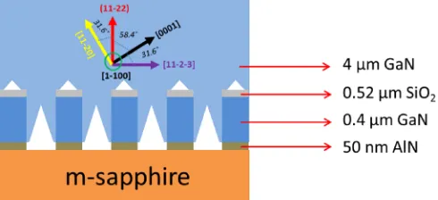
A single layer (11-22) semi-polar GaN template with a thickness of 1300 nm was grown onm-plane sapphire using a high temperature AlN buffer by metal organic chemical vapour deposition (MOCVD). Mask-patterned micro-rod arrays were then fabricated on the (11-22) GaN template for subsequent overgrowth. A detailed description of the growth and fabrication processes and their optimisation is given elsewhere.27 Here, we briefly describe the mask and micro-rod fabrication processes. First, a 500 nm SiO2 layer was
deposited by plasma enhanced chemical vapour deposition, followed by a standard photolithography patterning process and dry etching processes, using inductively coupled reactive plasma and reactive ion etching techniques, to produce regu-larly arrayed SiO2 micro-rods. The SiO2 micro-rods then
serve as a mask during a second etching step which produces GaN micro-rods with SiO2 remaining on the top of each
rod. The diameter, spacing, and height of the micro-rods can be controlled, and for the sample reported here (see Fig.1), the diameter and the spacing (edge to edge along the [1-100] direction or [-1-123] direction) of the micro-rods are both 5lm, and the height of the rods is 0.4lm. The semi-polar GaN template with the micro-rod array was sub-sequently reloaded into the MOCVD chamber for over-growth with a over-growth temperature, V/III ratio, and pressure
at 1120C, 1600, and 75 Torr, respectively. The overgrowth initiates from the exposed sidewalls of the micro-rods, and the lateral growth is dominated by the growth along the [0001] and [11-20] directions. After the coalescence of the [0001] and [11-20] growth facets, the GaN growth tends to move upwards. When the thickness of the overgrown layer exceeds the height of the micro-rods, the growth begins to extend to cover the SiO2masks, and a second coalescence occurs over
the SiO2masks. Finally, a fully coalesced surface is obtained
with the overgrowth of4lm. Figure1shows the schematic of the structure of the sample investigated.
B. ECCI
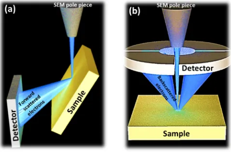
Detailed descriptions of the history and principle of ECCI for various material systems can be found in Refs.24 and28–30. Here, we briefly describe the principle and meth-odology used in our present work. There are two important conditions one has to fulfil to obtain ECC images. (1) Optimising the position of the sample with respect to the incident electron beam to obtain an appropriate channelling condition and (2) adjusting the detector position with respect to the sample to optimise the collection angle of the scattered electrons. The combination of a high brightness electron beam source (nanoamps or higher) with a low divergence angle (of the order of a few mrad) and a small spot size (nanometres) is a prerequisite. In addition, a good backscat-ter electron detector, ideally with an inbuilt preamplifier and an external amplifier, will greatly enhance the images obtained using ECCI.
[image:2.612.316.561.64.176.2]diode or diodes placed on/under the pole piece of the SEM).30,31 Figures 2(a) and 2(b) show schematics of the forescatter geometry and the backscatter geometry, respec-tively. The backscatter geometry has the advantage that large samples, e.g., a full semiconductor wafer (depending on the size of the SEM chamber), may be imaged and the results obtained may be more easily compared to a TEM diffraction image. The forescatter geometry requires tilt correction of the acquired images but provides a larger sig-nal and, therefore, channelling images with superior sigsig-nal to noise. We show the application of both geometries in our present work. An FEI Sirion 200 Schottky FEG–SEM was used to perform ECCI in the forescatter geometry, and the images were acquired using a 30 keV electron beam. We have used a FEI Quanta 250 FEG-SEM to perform ECCI in the backscatter geometry. For the ECCI images acquired in this geometry, we used a 20 keV electron beam.
III. RESULTS AND DISCUSSION
The most common extended defects in conventional c-plane oriented nitrides are perfect TDs of edge (a-type), screw (c-type), and mixed (aþc) types with the Burgers vectors (b) of 1/3h11-20i,h0001i, and 1/3h11-23i, respec-tively.32But in the case of semi-polar nitrides, in addition to perfect TDs, Shockley partials of b¼1/3h1-100i, Frank partials of b¼1/2h0001i, and Frank-Shockley partials of b¼1/ 6h20-23ihave also been reported. Stacking faults (SFs) in the basal plane with the displacement vectors R¼1/3h1-100i
(I1type), 1/6h20-23i(I2type), and 1/2h0001i(E type) as well
as in prismatic planes with R¼1/2h1-101iand 1/6h20-23iare also observed.32 In the case of semi-polar based nitride heterostructures, misfit dislocations of the edge type with b¼1/ 3h2-1-13i, formed at heterointerfaces, have also been reported recently.33The majority of reported BSFs are I1type, and the
associated partial dislocations (PDs) are of the Frank–Shockley type with b¼1/6h20-23i. In this work, we will focus on the total density of TDs reaching the surface without identifying their types, and we assume that the imaged BSFs are of the I1
type due to their lowest formation energy.34,35
A. Imaging of TDs in (11-22) GaN
In ECCI, individual vertical TDs appear as spots with black-white (B-W) contrast,36 and this is shown in the expanded excerpt of Fig.3, highlighted by a solid circle. The observed B-W contrast is a result of the strain fields around the dislocation. For materials with a wurtzite crystal struc-ture such as GaN, we have previously developed a simple geometric procedure to identify a given perfect TD as edge, screw, or mixed type by exploiting differences in the direc-tion of the B-W contrast between two ECC images acquired under near 2-beam conditions from two symmetrically equivalent crystal planes whose diffraction vector (g) is at 120 to each other, where g was determined through the acquisition of electron channelling patterns (ECPs).36 In the present case, we were not able to acquire ECPs due to the sample’s uneven surface morphology. However, we were able to exploit the sample’s surface morphology and the results obtained from previous TEM measurements,27to ori-ent the sample and select the diffraction conditions to maxi-mise channelling contrast or (and thus image) BSFs as well as TDs.
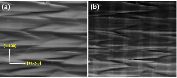
For the large area ECC image in Fig. 3, in addition to the diffraction contrast, there is also strong topography asso-ciated with the sample surface. The arrow head features (also referred to as chevrons) along the [-1-123] direction are com-monly observed in semi-polar nitride structures which have been grown using overgrowth techniques.37 Chevrons form due to imperfect coalescence during the overgrowth stage when two growth fronts with different growth rates meet. More information about the chevrons and their impact on optical properties can be found elsewhere.38The other strik-ing feature one can notice from Fig.3is the periodic arrange-ment of groups (clusters) of dislocations (see the five solid circles) where the centre to centre distance between the clus-ters of dislocation is 5lm, which is the spacing between the micro-rod arrays. Hence, the clustering of dislocations is related to the overgrowth on the micro-rod template. In addi-tion to clustering of dislocaaddi-tions, there are also addiaddi-tional random dislocations. In order to reliably estimate the TD density in this sample, we have separated the extended defect regions into two, areas of randomly distributed TDs (regions with fewer TDs) and clustered TDs. The circles drawn in Fig.3have an area of5lm2, corresponding to the spacing
[image:3.612.55.294.582.739.2]FIG. 2. Experimental setup: (a) forescatter geometry and (b) backscatter geometry.
[image:3.612.316.561.600.713.2]of the micro-rods. By simply counting the dislocations in the clustered regions (averaged over five regions), we have esti-mated the TD density to be8108cm2. For the regions with random TDs, the average dislocation density was esti-mated to be2108cm2. Averaging over a larger area of
200lm2(including the clustered and randomly distributed regions), we can estimate the average dislocation density for the overgrown thin film sample to be5108cm2. This is consistent with our previous plan view TEM studies39(data not shown here) which reveal the average TD density to be
4.2108cm2.
B. Imaging of BSFs in (11-22) GaN
Diffraction contrast at a stacking fault arises due to the displacement of the reflecting planes relative to each other above and below the fault plane. One can quantify this dis-placement by a vector R (disdis-placement vector) defined as the shear parallel to the fault of the portion of the crystal below the fault relative to that above the fault. By choosing the appropriate g, it is possible to maximise (when g is parallel to R) and minimise (when g is perpendicular to R) the stack-ing fault contrast in diffraction contrast imagstack-ing techni-ques.40 In order to visualise and maximise the contrast associated with stacking faults, one has to choose the condi-tion g. R¼0 or an integer.41In the case of plan-view TEM imaging of BSFs in (11-22) GaN, generally, the specimen is
[image:4.612.51.408.62.206.2]tilted to32to the [-1-120] zone-axis from the surface nor-mal with the diffraction vector g¼(10-10).39We have used a similar approach for imaging and maximising the contrast for BSFs in our samples. The ECCI shown in Fig. 4(a) is taken using the conventional forescatter geometry with a sample tilt of32and acquiring an ECC image when good contrast for BSFs was observed. It was not possible to select a precise g by acquiring ECPs in this case due to the sam-ple’s surface morphology. If the sample is rotated by 0.2, contrast reversal for BSFs can be seen in Fig.4(b). The con-trast reversal in this case may well be due to the deviation from the exact Bragg condition or due to a different g being selected.20Considering that the contrast reversal is observed for just a 0.2of rotation, it is more likely to be due to a devi-ation from the Bragg condition for diffraction. While the contrast reversal has been exploited to differentiate between the TD types in previous ECCI studies,36it is also quite use-ful as a tool to differentiate between diffraction contrast and topographic contrast. It is worth noting in Fig.4that the con-trast reversal associated with the BSFs can be seen clearly by changing the channelling conditions (the angle between the electron beams and the crystal lattice), while the topographic contrast associated with the surface features does not change. The topographic contrast can be seen clearly in Fig.5, which shows an secondary electron (SE) image and an ECC image from the same area of the sample with the sample in back-scatter geometry. The SE image in Fig. 5(a) shows FIG. 4. ECCI acquired in the forescat-ter geometry revealing basal plane stacking faults (BSFs). (a) Bright lines corresponding to BSFs showing con-trast reversal as seen in (b).
[image:4.612.52.406.577.733.2]predominantly the topographic contrast, whereas the ECC image in Fig.5(b) shows both diffraction and topographic contrast. Although one can observe the BSFs in the back-scatter geometry, the ECC image is quite noisy due to the lower backscattered electron yield at low sample tilt as well as due to the non-optimised diffraction conditions. In the present case, although the sample is not tilted with respect to the electron beam, the sample is mounted onto the alu-minium stub using silver paint which can cause a minor variation in the tilt. The suitable g necessary to maximise the contrast for BSF imaging in the backscatter geometry is yet to be undertaken. However, for samples where ECPs can be obtained, one can then choose any of the g vectors which are parallel to R to maximise the channelling con-trast for revealing BSFs. Please note that the channelling contrast is quite sensitive to small changes in the tilt and rotation as demonstrated in Fig.4. Since stacking faults are 2-D defects, their densities are typically represented as line densities (cm1) which are calculated by dividing the SF area by the probed volume of the sample. In the present case, the BSFs propagate through the entire sample (as determined from the cross sectional TEM,37data not shown here). Hence, we have counted the number of lines crossing
5lm along the [-1-123] direction from the FS geometry ECC images to estimate the BSF density. The average BSF line density is4104cm1. This is similar to the density estimated by plan-view TEM of 3104cm1. This is shown in Fig. 6, a bright field plan-view TEM image revealing BSFs as dark straight lines similar to what we have shown in the ECC images in Figs.4(a)and5(b).
IV. SUMMARY AND CONCLUSION
In summary, we have demonstrated that ECCI is an ideal and statistically reliable technique for rapid and non-destructive quantification of TD and BSF densities in semi-polar nitrides when compared to the presently available techniques. We were able to show similar information on BSFs provided by plan view TEM and have also shown the possibilities of imaging BSFs using both the ECCI geome-tries. The forescatter geometry has certain advantages such as accessing the diffraction conditions necessary to opti-mise contrast and thus quantify the extended defects as demonstrated in the present work; images may also be acquired with better signal to noise ratio. Nonetheless, the backscatter geometry is worthwhile, especially for looking at larger specimens and is a useful configuration for correla-tive microscopy.
ACKNOWLEDGMENTS
This work was supported by the EPSRC Project No. EP/ M015181/1, “Manufacturing of nano-engineered III-nitride.” The data associated with this paper can be found online under DOI http://dx.doi.org/10.15129/08835339-a263-4dab-a4dd-d0119dfe5ac8.
1
S. Chichibu, T. Azuhata, T. Sota, and S. Nakamura,Appl. Phys. Lett.69, 4188 (1996).
2P. Waltereit, O. Brandt, A. Trampert, H. T. Grahn, J. Menniger,
M. Ramsteiner, M. Reiche, and K. H. Ploog, Nature 406, 865 (2000).
3J. S. Speck and S. F. Chichibu,MRS Bull.34, 304 (2009).
4Y. Han, M. Caliebe, F. Hage, Q. Ramasse, M. Pristovsek, T. Zhu,
F. Scholz, and C. J. Humphreys, Phys. Status Solidi B 253, 834 (2016).
5F. Tendille, P. De Mierry, P. Vennegues, S. Chenot, and M. Teisseire, J. Cryst. Growth404, 177 (2014).
6
X. J. Ning, F. R. Chien, P. Pirouz, J. W. Yang, and M. Asif Khan,
J. Mater. Res.11, 580 (1996).
7D. C. Look and J. R. Sizelove,Phys. Rev. Lett.82, 1237 (1999). 8
P. Vennegue`s, J. M. Chauveau, Z. Bougrioua, T. Zhu, D. Martin, and N. Grandjean,J. Appl. Phys.112, 113518 (2012).
9
P. Vennegue`s, Z. Bougrioua, and T. Guehne,Jpn. J. Appl. Phys., Part 1
46, 4089 (2007).
10
F. A. Ponce, D. Cherns, W. T. Young, and J. W. Steeds,Appl. Phys. Lett.
69, 770 (1996).
11
D. M. Follstaedt, N. A. Missert, D. D. Koleske, C. C. Mitchell, and K. C. Cross,Appl. Phys. Lett.83, 4797 (2003).
12
F. Wu, Y. D. Lin, A. Chakraborty, H. Ohta, S. P. DenBaars, S. Nakamura, and J. S. Speck,Appl. Phys. Lett.96, 231912 (2010).
13K. Suzuki, M. Ichihara, and S. Takeuchi,Jpn. J. Appl. Phys., Part 133,
1114 (1994).
14
V. M. Kaganer, O. Brandt, A. Trampert, and K. H. Ploog,Phys. Rev. B
72, 045423 (2005).
15M. B. McLaurin, A. Hirai, E. Young, F. Wu, and J. Speck,Jpn. J. Appl. Phys., Part 147, 5429 (2008).
16
M. A. Moram, C. F. Johnston, J. L. Hollander, M. J. Kappers, and C. J. Humphreys,J. Appl. Phys.105, 113501 (2009).
17V. Holy, D. Kriegner, A. Lesnik, J. Bl€asing, M. Wieneke, A. Dadgar, and
P. Harcuba,Appl. Phys. Lett.110, 121905 (2017).
18
A. Davtyanet al.,J. Synchrotron Radiat.24, 981 (2017).
19
C. Trager-Cowan, F. Sweeney, P. W. Trimby, A. P. Day, A. Gholinia, N.-H. Schmidt, P. J. Parbrook, A. J. Wilkinson, and I. M. Watson,Phys. Rev. B75, 085301 (2007).
20
Y. N. Picard and M. E. Twigg,J. Appl. Phys.104, 124906 (2008).
21
S. D. Carnevale, J. I. Deitz, J. A. Carlin, Y. N. Picard, M. De Graef, S. A. Ringel, and T. J. Grassman,Appl. Phys. Lett.104, 232111 (2014).
22E. D. Le Boulbaret al.,J. Cryst. Growth
466, 30 (2017).
23
A. Vilalta-Clemente, G. Naresh-Kumar, M. Nouf-Allehiani, P. Gamarra, M. A. di Forte-Poisson, C. Trager-Cowan, and A. J. Wilkinson, Acta Mater.125, 125 (2017).
24
G. Naresh-Kumar, D. Thomson, M. Nouf-Allehiani, J. Bruckbauer, P. R. Edwards, B. Hourahine, R. W. Martin, and C. Trager-Cowan,Mater. Sci. Semicond. Process.47, 44 (2016).
25E. V. Lutsenkoet al.,J. Cryst. Growth434, 62 (2016). 26
Y. Gong, K. Xing, B. Xu, X. Yu, Z. Li, J. Bai, and T. Wang,ECS Trans.
66, 151 (2015).
27
Y. Zhang, J. Bai, Y. Hou, R. M. Smith, X. Yu, Y. Gong, and T. Wang,
AIP Adv.6, 025201 (2016).
28
D. C. Joy, D. E. Newbury, and D. L. Davidson,J. Appl. Phys.53, R81 (1982).
29A. J. Wilkinson and P. B. Hirsch,Micron28, 279 (1997). 30S. Zaefferer and N.-N. Elhami,Acta Mater.75, 20 (2014). 31
B. A. Simpkin and M. A. Crimp,Ultramicroscopy77, 65 (1999).
32
Y. A. R. Dasilva, M. P. Chauvat, P. Ruterana, L. Lahourcade, E. Monroy, and G. Nataf, J. Phys.: Condens. Matter. 22, 355802 (2010).
33
A. E. Romanov, E. C. Young, F. Wu, A. Tyagi, C. S. Gallinat, S. Nakamura, S. P. DenBaars, and J. S. Speck,J. Appl. Phys.109, 103522 (2011).
34Y. T. Rebaneet al.,Phys. Status Solidi A
[image:5.612.67.281.64.138.2]164, 141 (1997). FIG. 6. Plan view TEM image acquired using g¼(10-10) with the
35C. Stampfl and C. G. Van de Walle,Phys. Rev. B57, R15052 (1998). 36
G. Naresh-Kumar, B. Hourahine, P. R. Edwards, A. P. Day, A. Winkelmann, A. J. Wilkinson, P. J. Parbrook, G. England, and C. Trager-Cowan,Phys. Rev. Lett.108, 135503 (2012).
37M. Caliebeet al.,Phys. Status Solidi B253, 46 (2016). 38J. Bruckbaueret al.,Sci. Rep.
7, 10804 (2017).
39Y. Zhang, J. Bai, Y. Hou, X. Yu, Y. Gong, R. M. Smith, and T. Wang, Appl. Phys. Lett.109, 241906 (2016).
40
R. E. Smallman and A. H. Ngan,Modern Physical Metallurgy, 8th ed. (Butterworths-Heinemann, 2014), Chap. 5, pp. 219.
41B. H. Kong, Q. Sun, J. Han, I. H. Lee, and H. K. Cho,Appl. Surf. Sci.258,
![FIG. 6. Plan view TEM image acquired using g ¼ (10-10) with the speci-men viewed along the [-1-120] direction revealing basal plane stackingfaults.](https://thumb-us.123doks.com/thumbv2/123dok_us/1402215.93229/5.612.67.281.64.138/image-acquired-speci-viewed-direction-revealing-plane-stackingfaults.webp)