City, University of London Institutional Repository
Citation
:
Viphavakit, C., Patchoo, W., Boonruang, S., Themistos, C., Komodromos, M.,
Mohammed, W. S. & Rahman, B. M. (2017). Demonstration of Polarization-Independent
Surface Plasmon Resonance Polymer Waveguide for Refractive Index Sensing. Journal of
Lightwave Technology, 35(14), pp. 3012-3019. doi: 10.1109/JLT.2017.2711959
This is the accepted version of the paper.
This version of the publication may differ from the final published
version.
Permanent repository link:
http://openaccess.city.ac.uk/18501/
Link to published version
:
http://dx.doi.org/10.1109/JLT.2017.2711959
Copyright and reuse:
City Research Online aims to make research
outputs of City, University of London available to a wider audience.
Copyright and Moral Rights remain with the author(s) and/or copyright
holders. URLs from City Research Online may be freely distributed and
linked to.
City Research Online:
http://openaccess.city.ac.uk/
[email protected]
Demonstration of polarization-independent
surface plasmon resonance polymer
waveguide for refractive index sensing
C
HARUSLUKV
IPHAVAKIT,
1,*S
AKOOLKANB
OONRUANG,
2W
ISARNP
ATCHOO,
3C
HRISTOST
HEMISTOS,
4M
ICHAELK
OMODROMOS,
4W
ALEEDS.
M
OHAMMED,
3 ANDB.
M.
A
ZIZURR
AHMAN11
School of Mathematics, Computer Science and Engineering, City University London, Northampton Square, London EC1V 0HB, UK
2Photonics Technology Laboratory, Thailand National Electronics and Computer Technology Center
(NECTEC), KlongLuang, Pathumthani 10120, Thailand
3Center of Research in Optoelectronics, Communication and Control System (BU-CROCCS), Bangkok
University, Paholyotin Rd., Klong Luang, Pathumthani 12120, Thailand
4
Department of Electrical Engineering, Frederick University, 7 Y. Frederickou Str., Nicosia, 1036, Cyprus
Abstract: A gold-coated ormocomp waveguide is studied for it to be used for refractive index
sensing applications. The ormocomp waveguide is fabricated using the nanoimprint method with width and height of 10 µm. The waveguide is coated with gold of thickness 100 nm using the sputtering technique in order to introduce surface plasmon resonance at the sides and the top of the structure. Hence, a polarization-independent waveguide is achieved and the light confinement in both the TM and TE modes are studied. Supermodes occurring from the fundamental dielectric mode coupled with plasmonic supermode at the resonance peak are investigated. This paper presents the results obtained through simulations and also experimental validation. With this structure, there are two dielectric-plasmon supermodes with two resonance peaks separated by 50 nm. A red shift is observed when the refractive index of the cladding material increases. The cladding material includes water (n=1.333) and iso-propanol solutions with refractive indices of 1.344, 1.351 and 1.365. The gold-coated ormocomp waveguide has sensitivity of about 544.55 nm/RIU with a resolution of 5.3x10⁻³ RIU.
© 2016 Optical Society of America
OCIS codes: (130.5460) Polymer Waveguides; (240.6680) Surface Plasmon; (220.4000) Microstructure Fabrication; (000.4430) Numerical approximation and Analysis; (260.5430) Polarization; (280.4788) Optical Sensing and Sensors.
References
1. S. P. Chan, C. E. Png, S. T. Lim, G. T. Reed, and V. M. Passaro, "Single-mode and polarization-independent silicon-on-insulator waveguides with small cross section," Journal of Lightwave Technology 23, 2103 (2005). 2. W. R. Headley, G. T. Reed, S. Howe, A. Liu, and M. Paniccia, "Polarization-independent optical racetrack
resonators using rib waveguides on silicon-on-insulator," Applied Physics Letters 85, 5523-5525 (2004). 3. L. Vivien, S. Laval, B. Dumont, S. Lardenois, A. Koster, and E. Cassan, "Polarization-independent
single-mode rib waveguides on silicon-on-insulator for telecommunication wavelengths," Optics Communications
210, 43-49 (2002).
4. H. Ma, A. Y. Jen, and L. R. Dalton, "Polymer‐Based Optical Waveguides: Materials, Processing, and Devices," Advanced Materials 14, 1339-1365 (2002).
5. K.-H. Haas and K. Rose, "Hybrid inorganic/organic polymers with nanoscale building blocks: precursors, processing, properties and applications," Reviews on Advanced Materials Science 5, 47-52 (2003). 6. C. Sanchez, P. Belleville, M. Popall, and L. Nicole, "Applications of advanced hybrid organic–inorganic
nanomaterials: from laboratory to market," Chemical Society Reviews 40, 696-753 (2011).
8. M. Fukuda, T. Aihara, K. Yamaguchi, Y. Y. Ling, K. Miyaji, and M. Tohyama, "Light detection enhanced by surface plasmon resonance in metal film," Applied Physics Letters 96, 153107 (2010).
9. J. Homola, "Present and future of surface plasmon resonance biosensors," Analytical and Bioanalytical Chemistry 377, 528-539 (2003).
10. J. Homola, "Surface plasmon resonance sensors for detection of chemical and biological species," Chemical Reviews 108, 462-493 (2008).
11. C. Viphavakit, S. Boonruang, C. Themistos, M. Komodromos, W. S. Mohammed, and B. M. A. Rahman, "Surface plasmon resonance-enhanced light interaction in an integrated ormocomp nanowire," Optical and Quantum Electronics 48, 1-15 (2016).
12. F. Liu, Y. Rao, Y. Huang, W. Zhang, and J. Peng, "Coupling between long range surface plasmon polariton mode and dielectric waveguide mode," Applied Physics Letters 90, 141101 (2007).
13. M. Weisser, B. Menges, and S. Mittler-Neher, "Refractive index and thickness determination of monolayers by multi mode waveguide coupled surface plasmons," Sensors and Actuators B: Chemical 56, 189-197 (1999). 14. B. M. A. Rahman and J. B. Davies, "Finite-element solution of integrated optical waveguides," Journal of
Lightwave Technology 2, 682-688 (1984).
15. MicroresistTechnology, "UV-Curable Hybrid Polymers for Micro Optical Components," (April, 2014). 16. P. B. Johnson and R.W. Christy, "Optical constants of the noble metals," Physical Review B 6, 4370 (1972).
1. Introduction
Polarization-independent waveguides have been extensively studied and investigated for different applications [1-3]. There are many types of waveguides depending on the type of material used for their fabrication, such as semiconductor, glass and polymer. Silicon is the most common semiconductor used to fabricate waveguides. However, the fabrication of silicon waveguides requires cleanroom facilities and complex equipment which are costly. Glass waveguides are well-suited for simple optical detection due to their transparency, which means that there is low light absorption at the visible region. However, glass is fragile and vibration sensitive while the fabrication process of glass waveguides is difficult and very time consuming [4].
Polymer is a distinctive alternative material which can be used to build optical waveguides. Polymer waveguides have flexibility and biocompatibility [4]. Their fabrication process can be made simple and at a low cost. There are several types of polymers commonly used in photonics. Some examples are PDMS (polydimethylsiloxane), SU8, PMMA (polymethylmethacrylate) and ormocomp. The choice of what polymer to use depends on their properties and the requirements of a particular application.
Ormocomp is used in the fabrication of the waveguides in this work because it has a refractive index of 1.52 which is higher than the glass substrate (n=1.51). It is a hybrid polymer material consisting of an inorganic backbone and organic side groups at the molecular level, unlike composite materials which are mixtures at the macroscopic level [5]. Hence, the ormocomp is a homogeneous material that combines the properties of different material classes. Ormocomp obtains its flexibility and UV-curable property from the properties of organic polymers. The hardness and the chemical and thermal stability are obtained from the properties of ceramics whereas the transparency comes from the properties of glass. Ormocomp is also known to have an easy and low processing cost using the nanoimprint technique [6, 7].
The polarization-independent gold-coated ormocomp waveguides have been studied both through numerical simulations and experimentally. A full vectorial H-field finite element method (FEM) is used as a numerical tool to simulate the optical modes in the waveguide structure involving the effective index, resonance wavelength and its shift in different cladding materials such as water (n=1.333) and iso-propanol solutions (n=1.344, 1.351 and 1.365). An arrangement is set up to image the optical output signal and its transmission spectrum, thus showing the experimental resonance wavelength for each cladding material. A comparison of the resonance wavelengths, where the coupling between the dielectric mode and the plasmonic supermodes occurs, from the simulations and experiment measurements are presented. The sensitivity of the fabricated waveguides and their resolutions are also calculated.
2. Waveguide fabrication
The ormocomp waveguides are fabricated using the nanoimprint method which is a simple and low cost technique to transfer the waveguide pattern from a hard mold onto the ormocomp layer, which is a UV-curable hybrid polymer. In this work, silicon waveguides are used as the hard mold for the nanoimprint. The silicon waveguides are usually fabricated using a photolithography technique.
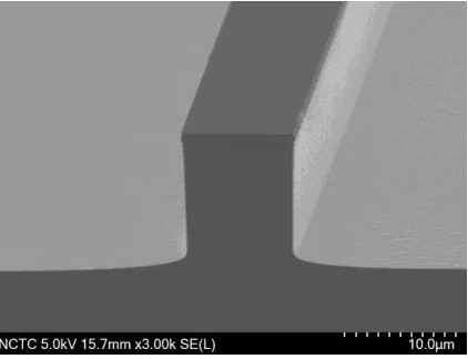
[image:4.612.202.413.456.618.2]There are three methods in the photolithography technique based on how the photo mask is placed, namely, contact photolithography, proximity lithography and projection photolithography. Contact photolithography is the simplest technique and it has the lowest manufacturing cost with high output solution of 1:1 magnification. Proximity photolithography has the lower resolution due to the diffraction which occurs due to the small gap between the optical mask and the photoresist layer. The projection photolithography has the highest resolution and de-magnification can be obtained allowing a sub-wavelength structure to be fabricated. However, only a small region on the photoresist layer is exposed at a time for projection photolithography, therefore a ‘stepper’ is required in order to move the substrate mechanically. In this work, the waveguide structure was chosen to have width and height of 10 µm in order to be fabricated using contact lithography to reduce the cost since sub-wavelength resolution is not required. An SEM image of the silicon waveguide fabricated using contact photolithography is shown in Fig. 1.
Fig. 1. SEM image of the cross section of the silicon waveguide with width and height of 10 µm fabricated using contact photolithography.
and curing agent (liquid) with a ratio of 7:1 by weight. The ratio can be varied depending on the required hardness of the PDMS mold. Liquid PDMS applied on the silicon mold has to be cured in a furnace at T=100C for 2 hours before it can be removed. Then, the PDMS soft mold is stamped on the ormocomp layer and cured with UV light for 5 minutes. Following the curing process, the ormocomp layer is hardened and the PDMS can be detached from the ormocomp. The nanoimprint process to fabricate ormocomp waveguide is shown in Fig. 2(b). By using the nanoimprint method, clean room facilities are not required and mass production is possible.
Fig. 2. (a) Schematic of PDMS soft mold preparation process for the nanoimprint technique. (b) Schematic showing the process of the nanoimprint technique for the ormocomp waveguide fabrication.
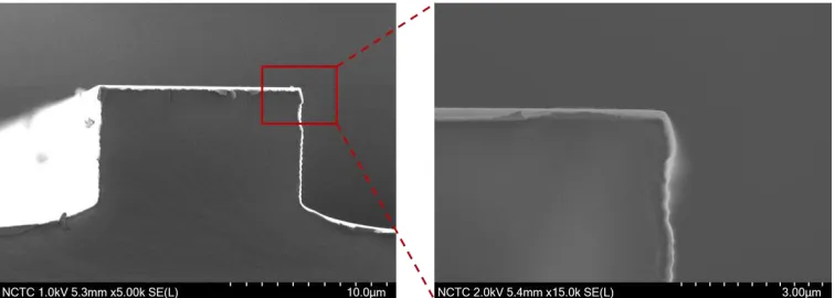
[image:5.612.138.471.198.364.2]The fabricated ormocomp waveguide is proposed to be used for refractive index sensing applications. The sensing area is at the core/cladding interface where the evanescent field interacts with the analyte material. When the core of the waveguide is large enough, then light is mostly confined in the core and thus only a small amount of the evanescent field is extended into the cladding region. In order to enhance the field at the core/cladding interface, a thin gold layer is coated onto the ormocomp waveguide to introduce surface plasmon resonance (SPR). Gold is coated using the sputtering technique. In this paper, chromium layer with thickness of 5 nm is coated first as an adhesion layer. The thickness of the gold is about 100 nm. An SEM image and a magnification of the gold-coated ormocomp waveguide are shown in Fig. 3.
[image:5.612.118.496.526.661.2]It can be seen from Fig. 3 that gold is coated both on the top surface and at the sides of the waveguide allowing electrons to be excited and oscillated both vertically (top surface) and horizontally (sides surface) at the interface between the dielectric and conductive materials. Hence, the waveguides can be polarization-independent. However, both quasi-TM (vertical polarization) and quasi-TE (horizontal polarization) modes are investigated in the numerical simulations by using the Finite Element Method (FEM) in order to study the characteristics and differences between the two polarization modes.
3. Simulation results
The Finite Element Method (FEM) is one of the most powerful numerical techniques used to analyze complex structure problems such as optical waveguides because of its accuracy, flexibility and versatility in the numerical analysis of optical waveguides. In the present work the full-vectorial H-field finite element formulation has been applied for the modal analysis of the quasi-TM and quasi-TE modes in the gold coated waveguide to determine the propagation characteristics of the coupled dielectric-plasmonic mode.
The principle of the FEM is to divide the complex structure into discrete elements, thus an equivalent discrete model for each element is constructed and all the elemental contributions to the system may be assembled to get an approximate solution of those differential or integral equation problems. Various types of elements can be used to assemble the continuum complex element, such as for example, triangles, rectangles, etc. However, the triangle shaped element is the most preferable because it has the simplest shape that can fit any complicated structures. The functional used to solve the problem is related to standard eigenvalue problems, and the modal characterization is obtained by minimizing the functional given in Eq. (1) [14]:
𝜔2=∫[(𝛻×H)∗∙𝜀−1(𝛻×H)+𝑝(𝛻×H)∗(𝛻×H)]𝑑𝑥𝑑𝑦
∫H∗∙𝜇H 𝑑𝑥𝑑𝑦 (1)
where H is the full vectorial magnetic field, * represents a complex conjugate and transpose,
𝜔 is the angular frequency of the wave, 𝜔2 is the eigenvalue, and 𝜀 and 𝜇 are the permittivity and permeability, respectively.
In this work, 64800 first order triangular elements are used to represent one half of the gold-coated waveguide structure. The waveguide has a width and height of 10 µm with 100 nm thick gold layer coated at the sides and on the top. With FEM, the size of the triangles can be varied for each individual part of the waveguide to achieve high computational efficiency. In this case, vertical resolution of 1.67 nm is obtained for the 100 nm thick gold layer. The ormocomp waveguide with refractive index of 1.52 has a high transparency, which means there is low light absorption at the visible wavelength [15]
.
Hence, the operating wavelength in this work is 400-700 nm. The complex refractive index of gold in the visible region is based on Johnson and Christy study [16]. For the sensing applications purposes, FEM is used to study the waveguide with different refractive indices of the cladding region. The refractive indices of the cladding region examined, have values of 1.333, 1.344, 1.351 and 1.365 which represent water and different concentrations of isopropanol solutions, respectively.From the SEM image of the fabricated gold-coated ormocomp waveguide, gold is coated both at the sides and on the top of the ormocomp. Therefore, the light propagating in the waveguide is studied for both the quasi-TM mode and quasi-TE modes using the full vectorial
H-field FEM. Changes in the effective index of a fundamental guided mode over the visible region for the quasi-TM and quasi-TE modes are shown in Fig. 4.
Fig. 4. Change of effective indices over the operating wavelength in the visible region for quasi-TM and quasi-TE modes.
The effective index variation graph shows particular peaks in some specific locations indicating the resonance phenomena. The effective index of the plasmonic mode is usually higher than the one of the dielectric mode. Therefore, the coupled mode between plasmonic and dielectric modes occurring at the resonance wavelength is higher than the dielectric mode alone at the non-resonance wavelengths. The thickness of the gold layer is 100 nm, which is thick enough to allow fundamental and higher order plasmonic modes to be supported. The different orders of the plasmonic modes can be coupled with the dielectric mode at different resonance wavelengths leading to several resonance peaks to occur. The thickness of the gold layer is fixed at 100 nm because with thinner gold layers, the plasmonic modes cannot occur. In addition, the effective index of the quasi-TE mode is slightly higher than the quasi-TM mode because there are two metal/cladding interfaces at the sides of the ormocomp waveguide for the quasi-TE mode but only one metal/cladding interface for the quasi-TM mode which is on the top of the waveguide. However, the resonance wavelengths occurring at both the quasi-TM and quasi-TE modes are almost identical.
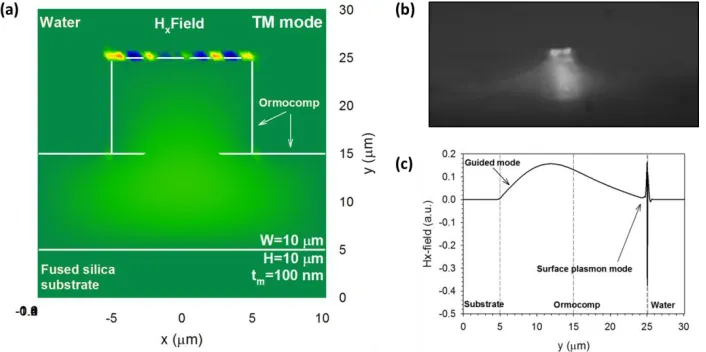
[image:7.612.194.420.91.251.2]The 2D optical fields obtained from the H-field FEM compared with the optical field images from the experiment and the field presented on the y-axis at the non-resonance wavelength and the resonance wavelength are shown in Fig. 5 and Fig. 6, respectively.
[image:7.612.138.484.487.661.2]From Fig. 5, only the dielectric mode is significant and confined in the core of the gold-coated ormocomp waveguide at the non-resonance wavelength. The ormocomp waveguide has a rib-structure, so some of the light at the core of the waveguide is extended into the rib layer as can be seen from the simulation in Fig. 5(a) and the image from CCD camera in the experimental setup in Fig. 5(b).
Fig. 6. Modal field profile excited in the ormocomp waveguide at the resonance wavelength from (a) FEM simulation and (b) experiment, and (c) Hx field of the coupled dielectric-plasmonic mode along the y-axis.
[image:8.612.134.487.161.337.2]Fig. 7. Graph of normalized power confinement in the sensing region of the ormocomp waveguide in water cladding calculated by using an in-house FEM program for quasi-TM and quasi-TE modes.
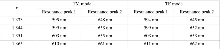
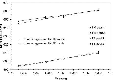
[image:9.612.193.423.91.252.2]The resonance wavelength can be indicated from power confinement in the sensing region graph where the peaks representing high power confinement are occurred. There are several peaks occurring due to the thickness of the gold layer. Considering the highest peak, there are two distinguished peaks for both the quasi-TM and the quasi-TE modes in the 100 nm gold layer. The resonance peak wavelengths of the quasi-TM and quasi-TE modes, of the gold-coated ormocomp waveguide, in different cladding materials, are presented in Table 1.
Table 1: Simulation results of the resonance peaks of the gold-coated ormocomp waveguide in different cladding materials for quasi-TM and quasi-TE modes.
n TM mode TE mode
Resonance peak 1 Resonance peak 2 Resonance peak 1 Resonance peak 2
1.333 595 nm 648 nm 594 nm 645 nm
1.344 599 nm 653 nm 599 nm 652 nm
1.351 603 nm 655 nm 603 nm 653 nm
1.365 610 nm 661 nm 611 nm 662 nm
[image:9.612.120.495.399.483.2]Fig. 8. Graph of the two resonance peaks obtained from the numerical simulations for each cladding material in both the quasi-TM and quasi-TE modes.
It can be observed from Fig. 8 that the resonance peak wavelength has a linear relationship with the refractive index of the cladding material for both the quasi-TM and quasi-TE modes. The regression lines of the quasi-TM modes, which are represented by solid lines, nearly perfectly fit the data with R-squared of 0.9929 and 0.9960 for resonance peaks 1 and 2, respectively. For the quasi-TE modes, the regression lines are represented by dashed lines with R-squared of 0.9755 and 0.9935 for resonance peaks 1 and 2, respectively. The slopes of the quasi-TE modes are slightly higher than the slopes of the quasi-TM mode for both resonance peaks which means that the quasi-TE mode has higher sensitivity compared to the quasi-TM mode. This is due to the larger surface area (double) at the sides of the waveguide compared to the surface area on the top.
4. Experimental results
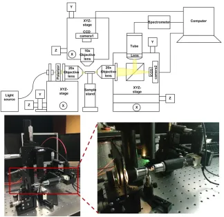
The experiment part includes an optical setup for imaging the optical output signal and monitoring the transmission spectrum from the gold-coated ormocomp waveguide to observe the resonance peak and its shift when there is a change in refractive index of the cladding material. The ormocomp waveguides with width and height of 10 µm are fabricated using the nanoimprint technique and coated with 100 nm gold layer using the sputtering method. The cladding materials in the experiment are water and iso-propanol solutions with different concentrations. The iso-propanol solutions are a mixture of water and iso-propanol with the volume ratio of 1:1, 1:3 and 1:5, providing the refractive indices of 1.365, 1351 and 1.344, respectively.
[image:10.612.190.421.90.255.2]Fig. 9. Optical setup for imaging and measuring the transmitted output signal.
Table 2: Experimental results of the resonance peaks of the gold-coated ormocomp waveguide in different cladding materials for the TM and TE modes.
n TM mode TE mode
Resonance peak 1 Resonance peak 2 Resonance peak 1 Resonance peak 2
1.333 592.3397 nm 649.2628 nm 598.0099 nm 646.8102 nm
1.344 601.8363 nm 654.3479 nm 600.6294 nm 649.9333 nm
1.351 606.3138 nm 656.3691 nm 601.6343 nm 654.1263 nm
1.365 609.9699 nm 660.5675 nm 612.5647 nm 659.6628 nm
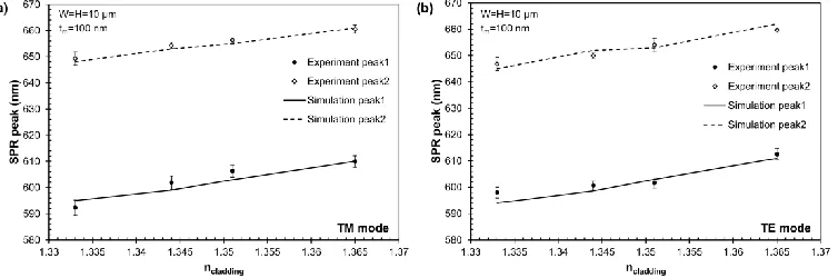
It can be seen that the resonance peaks occur in both the quasi-TM and quasi-TE modes at a similar wavelength. Hence, a polarization-independent gold-coated ormocomp waveguide has been successfully fabricated. The resonance peaks from Table 2 can be plotted so that we have a comparison with the resonance peaks obtained from the simulation using full vectorial
H-field FEM as shown in Fig. 10.
Fig. 10. Comparison of the resonance peaks obtained from the experiment and simulation for both TM and TE modes.
It can be seen from Fig. 10 that the resonance peaks obtained from the experiment have a similar trend compared to the simulation results. There are two different resonance peaks in both the experimental and simulation results, which means that there are two different plasmonic supermodes that are coupled with the dielectric mode. The two resonance peaks are located about 50 nm away from each other. The quasi-TM and quasi-TE mode have similar resonance wavelengths so the polarization in the experiment can be removed because the waveguides are polarization independent. Both experimental and simulation results show a redshift when the refractive index of the cladding material is increased.
To use this gold-coated ormocomp waveguide for refractive index sensing applications, the sensitivity is calculated from the linear regression of the experimental results and it is found to be 544.55 nm/RIU with resolution 5.3x10⁻³ RIU. The sensitivity and resolution of the waveguide can be further improved by optimizing the dimensions of the waveguide itself and the thickness of the gold layer. In addition, surface roughness is also considered to be one of the important parameters to improve sensitivity and resolution.
5. Summary
[image:12.612.121.498.278.403.2]