ELECTRICAL CHARACTERISTICS OF HIGH-K
DIELECTRICS FOR THE 19NM GATE LENGTH NMOS
DEVICE
NUR FATIN BINTI MOHD SABKI
This Reported Is Submitted In Partial Fulfillment Of Requirements For The Bachelor Degree Of Electronic Engineering (Computer Engineering)
Fakulti Kejuruteraan Elektronik dan kejuruteraan Komputer Universiti Teknikal Malaysia Melaka
iii “I hereby declare that the work in this project is my own except for summaries and
quotations which have been duly acknowledge.”
Signature : ...
Author : NUR FATIN BINTI MOHD SABKI
v For my beloved father, Mohd Sabki Ibrahim, my beloved mother Norhayati Mohd Lod and
vi ACKNOWLEDGEMENT
I feel very grateful toward Allah the Almighty for His blissful blessings in completing this thesis for my final project year project. I would like to thank for those whom involved directly and indirectly help making sure the sucess of my project
First and foremost I offer my sincerest gratitude to my supervisor Dr. Fauziyah Salehuddin for the help and effort she put through in completing this project. Another thank you notes for supporting me with her patience and knowledge whilst allowing me the room to work in my own way. I attribute the level of my bachelor degree to her encouragement and effort which without her this thesis too would not have been completed or wirtten. One simply could not wish for a better or friendlier supervisor.
I am also indebted to many friends who support me through thick and thin. Some of them offered a hand and kindness that can’t be paid for my entire life.
vii ABSTRACT
Aggressive scaling of n-channel metal oxide semiconductor (NMOS) device will increase the transistor density and performance. However, continual gate oxide scaling will require high-k gate dielectric, since the leakage current (IOFF) is increasing with
reducing physical thickness of gate oxide (SiO2). In this project, the effect of high-k
dielectrics for electrical characteristic in 19nm NMOS device were investigated. The two electrical characteristics that were considered are threshold voltage (VTH) and IOFF.
The device was virtual fabricated by using the ATHENA simulation module while the electrical characteristic response was stimulated using ATLAS module. The
performance of Titanium Oxide (TiO2) and Hafnium Oxide (HfO2) as high-k dielectric
materials with different metal gates such as Tungsten Silicides (WSix) and Titanium
Silicides (TiSix) have been made. As conclusion, the TiO2 has been recognized to be
the most suitable high-k dielectric material for metal gate, WSix. This is because
TiO2/WSix device has the lowest leakage current (1.92pA/µm) and the highest drive
current (578.8µA/µm) if compare with other devices include SiO2/Poly device. The
result obtained are well within International Technology Roadmap Semiconductor
(ITRS) prediction for the year 2015. Moreover, the TiO2/WSix device has an excellent
viii ABSTRAK
Pengecilan agresif peranti n-saluran logam oksida semikonduktor saluran -n(NMOS) akan meningkatkan ketumpatan transistor dan prestasi.Walaubagaimanapun,
pengecilan beterusan get oksida akan memerlukan high-k get dielektrik, kerana arus
bocor (IOFF) semakin meningkat dengan mengurangkan ketebalan fizikal get oksida
(SiO2). Dalam projek ini, kesan dielektrik high k untuk ciri elektrik bagi peranti
NMOS 19nm telah disiasat. Kedua-dua ciri-ciri elektrik yang dipertimbangkan adalah
ambang voltan (VTH) dan IOFF. Peranti telah difabrikasi secara maya menggunakan
modul simulasi ATHENA manakala sambutan ciri elektrik dirangsang menggunakan
modul ATLAS. Prestasi Titanium Oxide (TiO2) dan Hafnium Oxide (HfO2) sebagai
bahan high-k dengan get logam yang berbeza seperti Tungsten Silicides (WSix) dan
Titanium Silicides (TiSix) telah dibuat. Sebagai kesimpulan, TiO2 telah diiktiraf untuk
sebagai bahan high-k paling sesuai untuk get logam, WSix. Ini adalah kerana peranti
TiO2/WSix mempunyai arus bocor paling rendah (1.92pA/µm) dan arus salir yang
tinggi (578.8μA/µm) jika dibandingkan dengan peranti lain termasuk peranti
SiO2/Poli. Hasil lingkungan International Technology Roadmap Semiconductor
(ITRS)2013 ramalan bagi tahun 2015. Selain itu, peranti TiO2/WSix mempunyai
ix CONTENTS
CHAP CONTENTS PAGES
VERIFICATION OF STATUS REPORT ii
WRITER’S DECLARATION iii
SUPERVISOR’S DECLARATION iv
DEDICATION v
ACKNOWLEDGEMENT vi
ABSTRACT vii
ABSTRAK viii
CONTENT ix
LIST OF FIGURES xii
LIST OF SHORTFORMS xv
1 INTRODUCTION
1.1 BACKGROUND 1
1.2 OBJECTIVE 2
1.3 PROBLEM STATEMENT 2
1.4 SCOPE OF PROJECT 2
1.5 REPORT STRUCTURE 3
2 LITERATURE REVIEW 4
2.1 INTRODUCTION 4
x
2.3 TYPES OF MOSFET 6
2.3.1 Depletion-mode mosfet 7
2.3.2 Enhancement-mode mosfet 9
2.4 NMOS TRANSISTOR 10
2.5 SCALING 11
2.5.1 SHORT CHANNEL EFFECT 12
2.5.1.1Subtreshold current 13
2.5.1.2 Gate oxide tunneling current 13
2.6 HIGH- K MATERIAL 14
2.7 METAL GATE ELECTRODES 15
2.8 EQUIVALENT OXIDE THICKNESS (EOT) 16
3 METHODOLOGY 18
3.1 INTRODUCTION 18
3.2 SIMULATION USING TCAD 18
3.2.1 Atlas simulator 20
3.2.2 Athena simulator 20
3.3 ATHENA – FABRICATION STEPS OF 19NM NMOS
TRANSISTOR WITH HIGH-K
21
3.3.1 Mesh and substrate material establishment 22
3.3.2 Well Oxidation 23
3.3.3 Trenching and Gate Oxide growth 24
3.3.4 Threshold voltage adjustment implantation 25
3.3.5 High –k dielectric deposition 26
3.3.6 Halo implantation 28
3.3.7 Sidewall spacer 29
3.3.8 Source/drain implantation 30
3.3.9 PECVD & BPSG Oxide deposition 31
3.3.10 Pattern Source and Drain contact and compensate implantation
32
xi
3.3.12 Aluminium Etching 34
4 RESULT AND ANALYSIS 36
4.1 ELECTION OF HIGH K MATERIAL 36
4.2 SIMULATION RESULT OF STRUCTURE 37
4.2.1 Simulation result of structure and graph of Poly electrode
37
4.2.2 Graph of high-k material and metal gate and simulation result of structure.
38
4.2.2.1 Titanium oxide as high –k dielectric and titanium silicide as metal gate.
39
4.2.2.2 Hafnium as high –k dielectric and Titanium
silicide as metal gate 41
4.2.2.3 Titanium oxide as high –k dielectric and Tungsten silicide as metal gate.
43
4.2.2.4 Hafnium as high –k dielectric and Tungsten
silicide as metal gate. 45
4.3 ANALYSIS THE EFFECT OF HIGH-K DIELECTRICS
FOR ELECTRICAL CHARACTERISTIC OF 19NM NMOS DEVICES.
47
5 CONCLUSION AND FUTURE WORK 54
5.1 CONCLUSION 54
5.2 RECOMMENDATION AND FUTURE DEVELOPMENT 55
xii FIGURE LISTS
CONTENTS PAGES
Figure 2.1: MOSFET Structure 6
Figure 2.2: Channel and Symbols of n-channel MOSFET and p-channel MOSFET
7
Figure 2.3: ID-VDS graph n-channel MOSFET 8
Figure 2.4: Id-Vds graph N-Channel MOSFET 10
Figure 2.5 : Physical structure of the enhancement-type NMOS transistor
11
Figure 3.1: Flow of the method that use to design NMOS devices with high-k material
19
Figure 3.2: Simulation Using TCAD 20
Figure 3.3: Flowchart for n-channel MOSFET device with the High-K
21
Figure 3.4: P type substrate doping concentration 22
Figure 3.5: Source code to build the P-type substrate structure 22
Figure 3.6: 19nm structures after oxide deposition 23
Figure 3.7: source code to develop p-well oxidation 23
Figure 3.8: 19nm NMOS structure after gate oxide growth 24
Figure 3.9: Source code to do gate oxide growth process 25
Figure 3.10: 19nm NMOS structure after Vth adjusment implantation
26
Figure 3.11: Source code to do Vth adjustment implantation process
26
Figure 3.12: 19nm NMOS structure after high-k deposition 27
xiii
Figure 3.14: Source code to do halo implantation process 28
Figure 3.15: 19nm structure NMOS structure after halo implantation
28
Figure 3.16: 19nm NMOS structure after sidewall spacer 29
Figure 3.17: Source code to do sidewall spacer process 29
Figure 3.18: 19nm NMOS structure after source/drain implantation
30
Figure 3.19: Source code to do source/drain implantation process
30
Figure 3.20: 19nm NMOS structure after PECVD & BPSG Oxide deposition
31
Figure 3.21: Source code to do PECVD & BPSG Oxide deposition process
31
Figure 3.22: 19nm NMOS structure after Pattern Source and Drain contact and compensate implantation process
32
Figure 3.23: Source code to do Pattern Source and Drain contact and compensate implantation process
33
Figure 3.24: 19nm NMOS structure after Aluminium metallization
34
Figure 3.25: Source code to do Aluminium metallization process
34
Figure 3.26: 19nm NMOS structure after aluminium etching 35
Figure 3.27: Source code to do Aluminium Etching process 35
Figure 4.1: 19nm NMOS Structure with Polysilicon and Silicon Oxide
38
Figure 4.2 The Id–Vg overlay each device with different materials of high-K and different metal gate
39
Figure 4.3: 19nm NMOS Structure with titanium oxide as high –k dielectric and titanium silicide as metal gate.
40
Figure 4.4: The graph of ID versus VG for NMOS 19nm with
titanium oxide as high –k dielectric and titanium silicide as metal gate device.
xiv
Figure 4.5 : The Extract of Atlas Simulation Result Windows 41
Figure 4.6: 19nm NMOS Structure with hafnium as high –k dielectric and titanium silicide as metal gate.
42
Figure 4.7: The graph of ID versus VG for NMOS 19nm with
hafnium as high –k dielectric and titanium silicide as metal gate device.
42
Figure 4.8 : The Extract of Atlas Simulation Result Windows 43
Figure 4.9: 19nm NMOS Structure with titanium oxide as high –k dielectric and tungsten silicide as metal gate.
44
Figure 4.10: The graph of ID versus VG for NMOS 19nm with
titanium oxide as high –k dielectric and tunsgten silicide as metal gate device.
44
Figure 4.11: The Extract of Atlas Simulation Result Windows 45
Figure 4.12: The 19nm NMOS Structure with hafnium as high –k dielectric and tungsten silicide as metal gate.
46
Figure 4.13: The graph of ID versus VG for NMOS 19nm with
hafnium as high –k dielectric and tunsgten silicide as metal gate device.
46
Figure 4.14: The Extract of Atlas Simulation Result Windows 47
Figure 4.15: ION for 19nm NMOS Devices 49
Figure 4.16: ION for HfO2 and TiO2 dielectrics with metal gate
TiSix
50
Figure 4.17: ION for HfO2 and TiO2 dielectrics with metal gate
WSix
50
Figure 4.18: Ioff current for NMOS Devices 51
Figure 4.19: IOFF for HfO2 and TiO2 dielectrics with metal gate
TiSix
52
Figure 4.20: IOFF for HfO2 and TiO2 dielectrics with metal gate
WSix
xv LIST OF SHORT FORM
SHORTFORM FULL WORDS
BF2 Boron Difluoride
BPSG Boron Phosphor Silicate Gate
CMOS Complementary Metal-Oxide-Semiconductor
CMP Chemical Mechanical Polishing
D Drain
DIBL Drain Induced lowering Barrier
G Gate
GIDL Gate Induced Drain Leakage
IC Integrated Circuit
𝐼𝐷 Drain Current
IMD Intel Metal Dielectric
ITRS International Technology Roadmap for Semiconductor
LPCVD Low Pressure Chemical Vapour Deposition
NMOS N Channel MOSFET
PMD Premetal Dielectric
S Source
SCE Short Channel Effect
TCAD Technology Computer Aided Design
𝑣𝐷 Drain Voltage
𝑣𝐷𝑆 Drain to Source Voltage
𝑣𝐺 Gate Voltage
𝑣𝐺𝑆 Gate To Source Voltage
xvi
𝑣𝑠𝑢𝑏 Sub Threshold Voltage
1 CHAPTER 1
INTRODUCTION
1.1 Background
With new technologies, many industries to rely on a manufacturing of smaller, faster, cheaper and good quality of the MOSFET. With increasing global competition, modern industries have to adapt their production process to be more efficient and competitive. In order to more advanced technologies have to employ to scale down the
MOSFET into nanoscale [1]. Silicon oxide (SiO2) has been used as the gate dielectric
material over the years. Nowadays, high-k dielectric is widely accepted as a better approach for the gate dielectric of the MOSFET.
In this project, the fundamental understanding of the physical and the electrical characteristics of the 19nm gate length NMOS device containing high dielectric constant will be investigated. For this project, the performance of high-k dielectric
Titanium Oxide (TiO2) will be compared with SiO2 as gate dielectric. Besides, design
2 1.2 Objectives of this project
The objectives of this project are:
i) To design the 19nm gate length NMOS device by using SILVACO
TCAD Tools.
ii) To analyze the effect of high-k dielectrics for electrical characteristic of
19nm NMOS devices.
iii) To compare the performance of Titanium Oxide (TiO2) and Hafnium
Oxide (HfO2) as high-k dielectric with Silicon Oxide (SiO2) dielectric
with different metal gate which are Titanium Silicides (TiSix) and
Tungsten Silides (WSix)
1.3 Problem Statement
In trend of global competition, modern industries have to adjust their production process to be more efficient and competitive. Regarding that, more advanced technologies have to employ to scale down the MOSFET into nanometer. A few
decades ago, SiO2 known as widely used as the gate dielectric material and it requires
the film thickness to be as thin. However, the further scaling of SiO2 is below 2nm
gate layer thickness which can result in a large increase of the leakage current and short channel effect. In order to overcome this problem, many researchers are focusing on the metal gate with high –k materials that have the ability to be integrated in MOSFET flow. Among the high-K materials are compatible with silicon and also materials have too low or high dielectrics constant may not be an adequate choice for
alternative gate dielectric [1]. Therefore, replacing the SiO2 with a high-K materials
allows increased gate capacitance [2].
1.4 Scope of Project
3 19nm gate length NMOS device will be learned through out of this project. During this project, TiO2 and HfO2 will be used as the material gate dielectric with gate oxide
thickness is scaled to get the same Equivalent Oxide Thickness (EOT) for physical models of 19nm NMOS. Besides, process design of the NMOS device also will be learned. Then, the virtual design and fabrication of the device will be performed by using Athena module. Meanwhile, electrical characteristic performance will be stimulated by using an Atlas module of SILVACO software.
1.5 Report Structure
This thesis is a combination of five chapters that contain the introduction, literature review, methodology, result and discussion and the last chapter is the conclusion and recommendation of the project.
Chapter 1 is an introduction to the project. In this chapter, we will explain the background and objectives of the project. The concept behind the project and an overall overview of the project also will be discussed within this chapter. Chapter 2 discuss about the literature review of the effect of high-k dielectric value based upon previous research done.
Chapter 3 will explain about the project methodologies of the project. This chapter will show the steps and flow for problem solving in such a specific method used to design and develop the NMOS MOSFET structure, also the other factor and characteristic need to be focused on.
4 CHAPTER 2
LITERATURE REVIEW
2.1 Introduction
MOSFET stands for Metal-Oxide Semiconductor Field-Effect-Transistor. MOS (Metal-Oxide-Semiconductor) shows the basic physical device materials. The metal is used for contact electrodes and interconnections, the oxide is present for barriers. For developing the characteristics the isolation and semiconductor substrate with a specified doping profile provides the necessary physics. A MOSFET is referred at as a unipolar device because the nature of its design it. Specifically, the majority carriers in the channel region can be of only one type (electrons or holes). The MOSFET with electrons as the majority carriers in the channel is entitled a n-channel MOSFET or NMOS. Similarly, the MOSFET with holes as the majority carriers in the channel is a p-channel MOSFET or PMOS [3].
5 the MOSFETs development at 10-micron gate length was a standard design goal [3]. This length would prove to decrease significantly as time past with engineers striving to increase speed and component count per unit area. The gate length (the natural measure of the device technology) has been reduced by a factor 2 about every 5 years [3]. Since 2001, when bulk MOSFET was fabricated with the technology node of 130 nm by Intel as Under this technology, the device was produced using gate length and oxide thickness of 60 nm and 1.5 nm respectively.
2.2 Basic Mosfet Structure
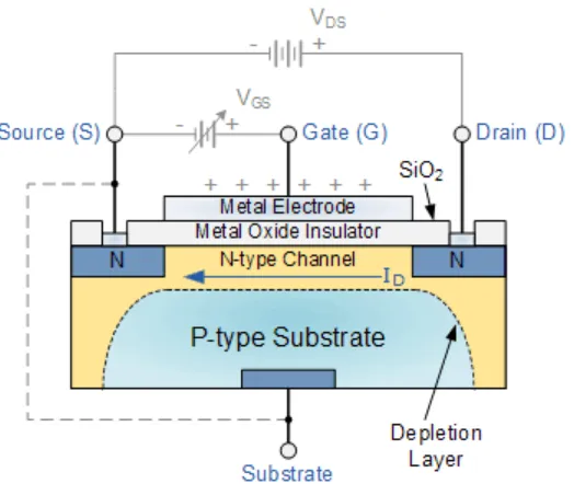
6 Figure 2.1: MOSFET Structure
2.3 Types of MOSFET
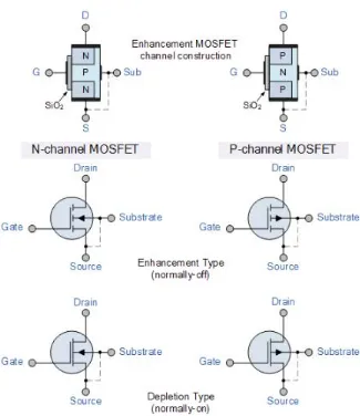
7 Figure 2.2: Channel and Symbols of n-channel MOSFET and p-channel MOSFET
2.3.1 Depletion-mode MOSFET
The Depletion-mode MOSFET, which is less common than the enhancement mode types is normally switched “ON” (conducting) without the application of a gate
bias voltage. That is the channel conducts when VGS=0V makes it a ‘normally-closed’
8
depletion MOS transistor, a negative gate-source voltage (-VGS) will deplete (hence its
name) the conductive channel of its free electrons switching the transistor ‘OFF’. Likewise for a p-channel depletion MOS transistor a positive gate-source voltage (+VGS) will deplete the channel of its free holes turning it ‘OFF’. In other words, for a
n-channel depletion mode MOSFET: +VGS means more electrons and more current.
Meanwhile a -VGS means less electrons and less current. The opposite is also true for
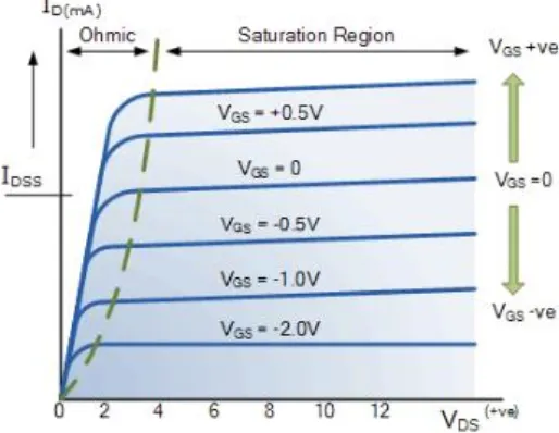
the p-channel types. Then the depletion mode MOSFET is equivalent to a ‘normally-closed’ switch. The depletion-mode MOSFET is constructed in a similar way to their JFET transistor counterparts were the drain-source channel is inherently conductive with the electrons and holes already present within the n-type or p-type channel. This doping of the channel produces a conducting path of low resistance between the Drain (D) and Source (S) with zero Gate (G) bias. Figure 2.3 shows graph of drain current
[image:24.595.189.446.392.591.2](ID) versus drain voltage (VDS) for n-channel MOSFET device [4].