Testability Trade-offs for BIST Data Paths
Nicola Nicolici and Bashir M. Al-Hashimi
Your Reference:JETT76601
Initial Submission - 20 July 2001
Revised Submission - 16 June 2003
Final Submission - 21 January 2004
CONTACT AUTHOR - NICOLA NICOLICI ([email protected])
Nicola Nicolici
Computer-Aided Design and Test Group Dept. of Electrical & Computer Engineering McMaster University
Hamilton, ON L8S 4K1, Canada Email: [email protected]
Phone: +1-905-525-9140 Extension 27598 Fax: +1-905-521-2922
Office: Communications Research Lab - Room 219 WWW: http://www.ece.mcmaster.ca/˜ nicola
Bashir M. Al-Hashimi
Electronic Systems Design Group
Dept. of Electronics and Computer Science University of Southampton
Southampton SO17 1BJ, U.K. Email: [email protected] Phone: +44-23-8059-3249 Fax: +44-23-8059-2901
Office: Mountbatten Building - Room 3021 WWW: http://www.ecs.soton.ac.uk/˜ bmah
Preliminary versions of this work have appeared in:
Testability Trade-offs for BIST Data Paths
Abstract
1
Introduction
The ever increasing demand for portable computing devices and wireless communication sys-tems requires low power very large scale integration (VLSI) circuits. Minimizing power dis-sipation during the VLSI design flow clearly increases lifetime and reliability of the circuit. Numerous techniques for low power VLSI circuit design have been reported [24] for comple-mentary metal-oxide semiconductor (CMOS) technology, where the dominant factor of power dissipation is dynamic power dissipation caused by switching activity [24]. While these tech-niques have successfully reduced the circuit power dissipation during functional operation, test-ing of such low power circuits has recently become an area of concern mainly because of the following two reasons. Firstly, it was reported in [29] that there is significantly higher switch-ing activity durswitch-ing testswitch-ing than durswitch-ing functional operation and hence higher power dissipation. This can decrease the reliability of the circuit under test (CUT) due to excessive temperature and current density which cannot be tolerated by circuits designed using power minimization tech-niques. Secondly, high switching activity during test application leads to manufacturing yield loss which can be explained as follows [28]. High switching activity during test application causes high rate of current flowing in power and ground lines leading to excessive power/ground noise and large resistive voltage drop. Resistive voltage drop caused by large maximum instan-taneous current flowing in the power lines is underestimated by state of the art approaches [26] since they assume signal correlations that are destroyed when employing design for test (DFT) methodologies, such as scan or built-in self-test (BIST). Therefore, high power/ground noise combined with large resistive voltage drop can erroneously change the logic state of circuit lines causing some good circuits to fail the test, leading to unnecessary loss of manufacturing yield. Consequently, addressing the problems associated with testing low power VLSI circuits has become an important issue. It is shown in this paper how power dissipation is related to different BIST parameters. Prior to explaining the motivational experimental results presented in this paper, the sources of higher power dissipation during test application are discussed and shortcomings of the previous approaches are outlined.
Power can be minimized during testing by reducing spurious transitions during test
ap-plication which do not carry any useful test operation. Many approaches have been
Higher power dissipation during test application caused by design techniques at the register-transfer level (RTL) of abstraction is due to the following. Systems which comprise high num-ber of memory elements and multi-functional execution units employ power conscious archi-tectural decisions such as power management, where blocks are not simultaneously activated during functional operation [3, 14]. Hence, inactive blocks do not contribute to dissipation during the functional operation. The fundamental premise for power management is that sys-tems and their components experience nonuniform workload during the functional operation [3]. However, such an assumption is not valid during test application due to the following rea-son. In order to minimize test application time when the system is in the test mode, concurrent execution of tests is required. This will result in substantially higher power dissipation dur-ing test application when compared to functional operation. To overcome the problem of high power dissipation during test application at RTL, numerous power-constrained test scheduling algorithms have been proposed under BIST environment [4, 5, 18, 25, 29]. However, the pre-vious power-constrained test scheduling algorithms are based on fixed test resource allocation, and therefore have considered only the two dimensional trade-off between test application time and power dissipation. Further, it has been shown that test synthesis and test scheduling are strictly interrelated [15, 22] justifying that fixed test resource formulation leads to inefficient exploration of the testable design space. So far, the interrelation between test synthesis and test scheduling has considered only the two dimensional trade-off between test application time and BIST area overhead. This two dimensional trade-off ignores the large variation in power dissi-pation for testable designs that are equivalent from test application time and BIST area overhead standpoint.
2
Experimental validation flow
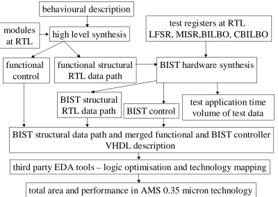
Section 2.1 provides an overview of the BIST embedding methodology. Section 2.2 presents the automated experimental validation flow for a large number of BIST RTL data paths, and section 2.3 gives an illustrative example of the trade-offs in a BIST data path. The objective of describing this automated experimental validation flow is to ex
2.1
Overview of BIST embedding methodology
In parallel BIST methodology, test patterns are applied to CUT every clock cycle which leads to a substantial reduction in test application time when compared to standard scan based DFT or scan BIST methodology [1]. BIST embedding is the parallel BIST methodology where each module is a test primitive in the sense that test patterns are generated and output responses are compressed using test registers for each module [15]. This methodology is particularly suitable for data path circuits described at register-transfer level of the VLSI design flow where modules are tested using test registers which are a subset of functional registers.
application time, BIST area overhead, and performance degradation, another important BIST parameter is volume of test data. Volume of test data affects storage requirements and shifting time required to shift in the seeds for TPGs and shift out the signatures stored in SAs. While volume of test data was not a concern in the past for small to medium sized circuits it is recently emerging as a problem for testers which need to change to support the large volume of test data [12].
According to the necessity for achieving the required test efficiency, power dissipation in BIST RTL data paths is classified into necessary and useless power dissipation [21].
Neces-sary power dissipation is the power dissipated in test registers and tested modules during each
test session and the power dissipated in test registers while shifting in seeds for test pattern generators and shifting out responses from signature analyzers. Necessary power dissipation is compulsory for achieving the required test efficiency, however, the useless power dissipation, defined in the following, must be eliminated. Useless power dissipation is the power dissipated in registers and untested modules due to spurious transitions which cannot be eliminated by any configuration of control signals of data path multiplexers.
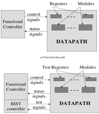
After test resources have been allocated (test synthesis) and test schedule has been generated (test scheduling) the final step is to synthesize a BIST controller that controls the execution of test sessions and shifts in the seeds for TPGs and shifts out the signatures stored in SAs. In order to achieve minimum area overhead, BIST controller is merged with the functional controller into a single control unit for the data path. Figure 1 shows the extention of a functional data path (Figure 1(a)) to a self-testable data path (Figure 1(b)) with merged functional and BIST controllers. A particular advantage of specifying a circuit at RTL is that control and status signals that operate the data path during the functional operation are merged and optimized with the test signals that operate the data path during testing.
2.2
Automated design space exploration
Prior to explaining the automated experimental validation flow, the size of the solution space is outlined. If for each input port of every data path module, l =1. . .2×nmod, where nmod is the
number of modules, there is an ml-to-1 multiplexer, then the total number of paths to drive test
patterns to data path modules is
2×nmod
∏
l=1
ml (it is assumed that there are 2 input ports for every
module). Similarly, if for each output port of every data path module, k=1. . .nmod, the fanout
is equal to mk, then the total number of paths to drive test responses to signature analyzers is nmod
∏
k=1
DATAPATH
Functional
Controller
Registers Modules
control
signals
status
signals
(a) Functional data path
DATAPATH
Functional
Controller
Test Registers Modules
control
signals
status
signals
BIST
controller
test
signals
[image:7.612.109.489.125.564.2](b) Testable data path
behavioural description
high level synthesis
functional structural
RTL data path
functional
control
BIST hardware synthesis
BIST structural
RTL data path
BIST control
BIST structural data path and merged functional and BIST controller
VHDL description
third party EDA tools – logic optimisation and technology mapping
total area and performance in AMS 0.35 micron technology
test registers at RTL
LFSR, MISR,BILBO, CBILBO
modules
at RTL
[image:8.612.113.513.36.320.2]test application time
volume of test data
Figure 2: Test application time, BIST area overhead, and performance estimation for BIST RTL data paths.
2×nmod
∏
l=1
ml× nmod
∏
k=1
mk. For example in the case of 32 point discrete cosine transform (DCT) data
path with 60 registers, 9 multipliers, and 12 adders, by analyzing the interconnection between modules and registers, the total size of the solution space is≈1023. Since plotting the entire so-lution space is beyond the computational capabilities of the state of the art computing resources, the results presented in sections 3, 4, and 5 have been obtained by randomly generating 33,500 BIST data paths which is a representative testable design space of the entire solution space. The random BIST data paths have been generated in such way that for each functional module input (output), a random register from the input (output) register set has been selected to be modified into an LFSR (MISR).
based on the following primitive polynomial: x8+x4+x3+x+1. For the purpose of plotting a representative statistical sample of the huge solution space, BIST hardware synthesis randomly assigns test pattern generators for left and right inputs of data path modules. Similarly, signature analyzers at the output of data path modules are randomly chosen from the output module set. Having obtained test hardware allocation, a test schedule is generated using the test scheduling algorithm reported in [7]. The test length for adders and multipliers is considered T+ =Tu,
and respectively T∗=4×Tu, where Tu=128 for achieving 100% fault coverage for 8 bit data
path modules. The output of BIST hardware synthesis are: test application time and volume of test data, BIST control, and BIST structural data path. The functional control, BIST control, and BIST structural data path are specified in VHDL and technology mapped using third party electronic design automation (EDA) tools into AMS 0.35 micron technology [2]. The results obtained after technology mapping provide total area in terms of square mils and performance in terms of clock frequency in MHz. BIST area overhead is computed by subtracting from the total area the area of the functional structural RTL data path where test registers and BIST con-trol are not inserted. It should be noted that BIST area overhead in terms of square mils reflects not only the additional test hardware required by test registers, but also the additional gates required to integrate the functional and BIST controller as outlined in Figure 1. The trade-offs between BIST parameters obtained using the experimental validation flow shown in Figure 2 are reported in the following sections.
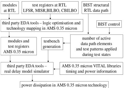
In order to compute the power dissipation reported, the experimental validation flow shown in Figure 3 is employed. The modules at RTL used by the high-level synthesis system, as shown in Figure 2, and test registers are synthesized and technology mapped into AMS 0.35 micron technology [2]. Having obtained the BIST structural data path and BIST control as described in Figure 2, the number of active data path elements, and the test patterns applied during each test state, serve as input for the generation of a testbench. The testbench consists of an activity
profile of all the data path elements in every test state which can either be a test application state
BIST control
BIST structural
RTL data path
number of active
data path elements
and test patterns applied
during test states
modules
at RTL
test registers at RTL
LFSR, MISR,BILBO, CBILBO
third party EDA tools – logic optimisation and
technology mapping in AMS 0.35 micron
modules and
test registers
AMS 0.35 micron
AMS 0.35 micron VITAL libraries
timing and power information
third party EDA tools –
real delay model simulator
power dissipation in AMS 0.35 micron technology
testbench
[image:10.612.110.511.34.319.2]generation
Figure 3: Power dissipation estimation for BIST RTL data paths.
P∗=11.5mW . Finally, the value of power dissipation is computed hierarchically by summing the power profile of active data path elements in every test state using the activity profile over the entire test application period. This hierarchical power dissipation computation provides a trade-off between the accuracy of low level power simulators and the computational time re-quired for the large sample of 33,500 testable designs for a complex circuit such as 32 point DCT.
2.3
An illustrative BIST data path example
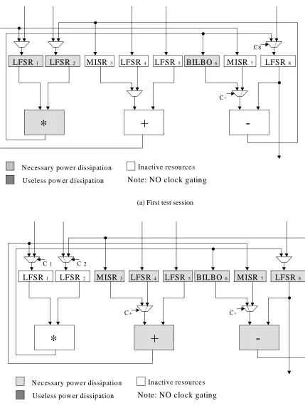
Prior to showing the trade-offs for 32 point DCT, this section gives an illustrative example explaining how different test register allocations determine variations in BIST area overhead and power dissipation. The data path comprises a multiplier, an adder and a subtracter and two BIST sessions are sufficient to complete its testing process, as explained in the following.
Consider the low power data path shown in Figures 4 and 5, where during the functional operation the multiplier∗ is never active at the same time as the adder(+)and the subtracter
session for the adder (+) and subtracter (−) (Figure 4(b)). The BIST RTL data path shown in Figure 4 is obtained such that a given power constraint derived from functional operation is not exceeded during test application. The main objective is to minimize BIST area overhead when having two separate test sessions. Figure 5 illustrates the BIST RTL data path in two test sessions when applying the power conscious test synthesis and scheduling detailed in [21]. The main objective of power conscious test synthesis and scheduling is to eliminate useless power dissipation, and then it uses BIST area overhead as a tie-breaking mechanism among alternative possible solutions. Power conscious test synthesis and scheduling leads to more test registers than when allocating test registers for minimum BIST area overhead. However, this is achieved with the benefit of eliminating useless power dissipation. It should be noted that the power constraint is exceeded in both test sessions in Figure 4. This is due to useless power dissipation shown in registers R3, R6 and subtracter(−)of Figure 4(a) and registers R3, R6 and multiplier
(∗)of Figure 4(b). Since the multiplier∗is never active at the same time as the adder(+)and the subtracter(−), the maximum power dissipated during the functional operation of the data path from Figure 4 can be considered 16.5mW (simultaneous activity of BILBO1, BILBO2, and
(∗)). Considering manufacturing process tolerance the power constraint during testing is set to 20mW . When ignoring useless power dissipation during test synthesis and scheduling power value for the first test session (Figure 4(a)) is 24.1mW , and 30.1mW for the second test session (Figure 4(b)). This shows that when ignoring useless power dissipation there is a violation of the power constraint and substantially higher power dissipation during testing. When employing power conscious test synthesis and scheduling the maximum power dissipated by the data path from Figure 5 can be considered 13.5mW (due to the simultaneous activity of LFSR1, LFSR2,
BILBO 1
*
BILBO 2 R 3 LFSR 4 LFSR 5 R 6 LFSR 7 BILBO 8
+
-Necessary power dissipation
Useless pow er dissipation Note: NO clock gating
C+ C
-Inactive resources
(a) First test session
BILBO 1
*
BILBO 2 R 3 LFSR 4 LFSR 5 R 6 LFSR 7 BILBO 8
+
-Necessary power dissipation
Useless pow er dissipation Note: NO clock gating
C+ C
-C 1 C 2
Inactive resources
[image:12.612.87.516.64.634.2](b) Second test session
LFSR 1
*
LFSR 2 M ISR 3 LFSR 4 LFSR 5 BILBO 6 M ISR 7 LFSR 8
+
-Necessary power dissipation
Useless pow er dissipation Note: NO clock gating
C
-C8
Inactive resources
(a) First test session
LFSR 1
*
LFSR 2 M ISR 3 LFSR 4 LFSR 5 BILBO 6 M ISR 7 LFSR 8
+
-Necessary power dissipation
Useless pow er dissipation Note: NO clock gating
C
-Inactive resources
C+
C 2
C 1
[image:13.612.88.517.62.635.2](b) Second test session
3
Test application time vs. BIST area overhead
Having described the experimental validation flow in section 2, this section discusses the two dimensional design space illustrating the relation between BIST area overhead and test applica-tion time.
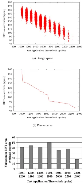
It can be clearly seen in Figure 6(a) that as test application time decreases there is an in-crease in BIST area overhead. Therefore, since BIST area overhead and test application time are traded-off one against each other, finding the set of optimal solutions is an multiobjective optimization problem [9]. In multiobjective optimization not a single optimal solution is tar-geted, but rather the Pareto set (Pareto curve) which is the set of all the feasible solutions whose vector of the multiple objectives is not dominated by the vector of any other solution. In the particular case of the two dimensional design space shown in Figure 6(a) a vector of the two objectives (BIST area overhead and test application time) is dominated by another vector if it has either lower test application time or BIST area overhead. The Pareto curve is shown in Fig-ure 6(b). It is interesting to note that there are many test resource allocations leading to equal values in test application time with significantly different values in BIST area overhead. For example, when test application time ranges between 1600 and 1800 clock cycles, the BIST area overhead varies approximately 50 square mils as shown in Figure 6(c). Figure 6 justifies the need of efficient testable design space exploration algorithms, to consciously account for the interrelation between test synthesis and test scheduling [15, 22]. However, trading-off only test application time and BIST area overhead will identify solutions belonging to the Pareto curve, which have high values in power dissipation.
4
Test application time vs. power dissipation
The main disadvantage of trading off only test application time and BIST area overhead is that testable data paths are selected without providing the flexibility of exploring alternative solu-tions in terms of power dissipation. Indeed, a large number of optimal or near-optimal solusolu-tions in terms of test application time and BIST area overhead may be found, but with different power dissipation. Thus, power dissipation is a new parameter which should be considered during testable design space exploration.
70 80 90 100 110 120 130 140 150 160 170 180
800 1000 1200 1400 1600 1800 2000 2200 2400 2600
BIST area overhead (sqmils)
test application time (clock cycles)
(a) Design space
70 80 90 100 110 120 130 140 150 160
800 1000 1200 1400 1600 1800 2000 2200 2400
BIST area overhead (sqmils)
test application time (clock cycles)
(b) Pareto curve
0 10 20 30 40 50 60 1000-1200 1200-1400 1400-1600 1600-1800 1800-2000 2000-2200 2200-2400 Test Application Time (clock cycles)
V a r ia ti o n i n B IS T a r e a o v e r h e a d ( sq m il )
[image:15.612.172.442.51.661.2](c) Variation in BIST area overhead
20 30 40 50 60 70 80 90 100 110 120 130
800 1000 1200 1400 1600 1800 2000 2200 2400 2600
power dissipation (mW)
test application time (clock cycles)
(a) Design space
20 30 40 50 60 70 80 90
800 1000 1200 1400 1600 1800 2000 2200
power dissipation (mW)
test application time (clock cycles)
(b) Pareto curve
0 10 20 30 40 50 60 70 80 1000-1200 1200-1400 1400-1600 1600-1800 1800-2000 2000-2200 2200-2400 Test Application Time (clock cycles)
V a ri a ti o n i n p o w er d is si p a ti o n (m W )
[image:16.612.167.449.51.649.2](c) Variation in power dissipation
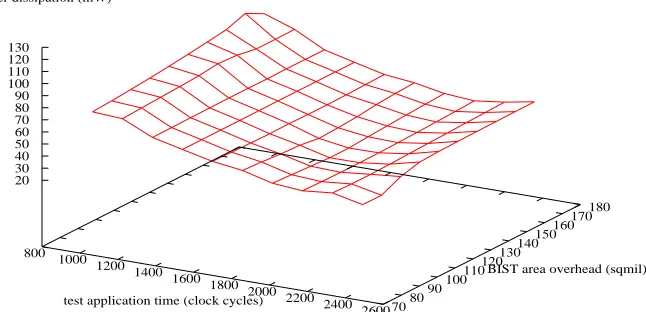
application under given power constraints [4, 5, 18, 25, 29]. The improvement can be achieved by lowering the power constraints and efficiently searching for high test concurrency, hence leading to simultaneous reduction in both test application time and power dissipation. Another interesting point is the variation in power dissipation. The different values in power dissipation during test application are not caused only by different values in BIST area overhead. Since power dissipation is dependent on switching activity of all the active elements during each test session, the variation in power dissipation is also due to useless power dissipation introduced in section 2.1. Therefore, unlike the case of BIST area overhead where the variation is equally distributed over different test application times (Figure 6(c)), the variation in power dissipa-tion increases as test applicadissipa-tion time decreases (Figure 7(c)), and can be explained as follows. When the number of test registers increases to improve the test concurrency (which is limited by test hardware sharing), the multiplexer configurations that can eliminate spurious transitions and hence useless power dissipation, vary significantly from one test register allocation to another, which is not the case for testable data paths with a small number of shared test registers. There-fore, when high test concurrency is aimed under given power constraints, one should carefully examine test register allocations to ensure that spurious activity is reduced as much as possible.
5
The case for three dimensional design space
800 1000
1200 1400
1600 1800
2000 2200
2400 2600 test application time (clock cycles) 708090
100110 120130
140150 160170
180
BIST area overhead (sqmil) 20
30 40 50 60 70 80 90 100 110 120 130
power dissipation (mW)
(a) Design space
800 1000
1200 1400
1600 1800
2000 2200
2400 2600 test application time (clock cycles) 7080
90 100 110120
130140 150160
BIST area overhead (sqmils) 20
30 40 50 60 70 80 90 100 110 120
power dissipation (mW)
[image:18.612.155.478.145.301.2](b) Pareto set
6
Conclusion
The demand for low power VLSI circuits will continue to increase in the future. Cost and life-time cycle of near future portable communications and computing systems will depend not only on VLSI circuits designed using low power synthesis techniques, but also on new DFT methods targeting power minimization during test application. This is because traditional DFT methods are not suitable for testing low power VLSI circuits leading to lower reliability and manufac-turing yield [28, 29]. This paper has focused on investigating testability trade-offs in BIST RTL data paths. It was shown that BIST area overhead, test application and power dissipation are strongly interrelated which justifies the need for exploring three dimensional testable design
space. The exhaustive experimental results presented in this paper further motivate the need for
new power conscious DFT methods, test synthesis and test scheduling algorithms for testing low power VLSI circuits [11, 19].
References
[1] M. Abramovici, M.A. Breuer, and A.D. Friedman. Digital Systems Testing and Testable
Design. IEEE Press, 1990.
[2] AMS. 0.35 Micron CMOS Process Parameters. Austria Mikro Systeme International AG, 1998.
[3] L. Benini, A. Bogliolo, and G. De Micheli. A survey of design techniques for system-level dynamic power management. IEEE Transactions on Very Large Scale Integration (VLSI)
Systems, 8(3):299–316, June 2000.
[4] K. Chakrabarty. Design of system-on-a-chip test access architectures under place-and-route and power constraints. In Proc. IEEE/ACM Design Automation Conference (DAC), pages 432–437, 2000.
[5] R.M. Chou, K.K. Saluja, and V.D. Agrawal. Scheduling tests for VLSI systems under power constraints. IEEE Transactions on Very Large Scale Integration (VLSI) Systems, 5(2):175–184, June 1997.
[6] F. Corno, M. Rebaudengo, M. Sonza Reorda, and M. Violante. Optimal vector selection for low power BIST. In IEEE International Symposium on Defect and Fault Tolerance in
[7] G.L. Craig, C.R. Kime, and K.K. Saluja. Test scheduling and control for VLSI built-in self-test. IEEE Transactions on Computers, 37(9):1099–1109, September 1988.
[8] V. Dabholkar, S. Chakravarty, I. Pomeranz, and S.M. Reddy. Techniques for minimizing power dissipation in scan and combinational circuits during test application. IEEE
Trans-actions on Computer-Aided Design of Integrated Circuits and Systems, 17(12):1325–1333,
December 1998.
[9] P. Dasgupta, P. P. Chakrabarti, and S. C. Desarkar. Multiobjective Heuristic Search :
An Introduction to Intelligent Search Methods for Multicriteria Optimization. Morgan
Kaufmann Pub., 1999.
[10] S. Gerstendorfer and H.J. Wunderlich. Minimized power consumption for scan-based BIST. Journal of Electronic Testing: Theory and Applications (JETTA), 16(3):203–212, June 2000.
[11] P. Girard. Low power testing of VLSI circuits: Problems and solutions. In First
Interna-tional Symposium on Quality of Electronic Design (ISQED), pages 173–180, 2000.
[12] R. Kapur and T.W. Williams. Tough challenges as design and test go nanometer.
Com-puter, 32(11):42–45, November 1999.
[13] P. Kollig and B.M. Al-Hashimi. A new approach to simultaneous scheduling, allocation and binding in high level synthesis. IEE Electronics Letters, 33(18):1516–1518, August 1997.
[14] G. Lakshminarayana, A. Raghunathan, N.K. Jha, and S. Dey. Power management in high level synthesis. IEEE Transactions on Very Large Scale Integration (VLSI) Systems, 7(1):7–15, March 1999.
[15] S.P. Lin, C.A. Njinda, and M.A. Breuer. Generating a family of testable designs using the BILBO methodology. Journal of Electronic Testing: Theory and Applications (JETTA), 4(2):71–89, 1993.
[16] S. Manich, A. Gabarro, M. Lopez, J. Figueras, P. Girard, L. Guiller, C. Landrault, S. Pravossoudovitch, P. Teixeira, and M. Santos. Low power BIST by filtering non-detecting vectors. Journal of Electronic Testing: Theory and Applications (JETTA),
16(3):193–202, June 2000.
[18] V. Muresan, V. Muresan, X. Wang, and M. Vladutiu. The left edge algorithm and the tree growing technique in block-test scheduling under power constraints. In Proc. of the 18th
IEEE VLSI Test Symposium, pages 417–422, 2000.
[19] N. Nicolici and B. M. Al-Hashimi. Power-Constrained Testing of VLSI Circuits. Kluwer Academic Publishers, Frontiers in Electronic Testing (FRET) Series, 2003.
[20] N. Nicolici and B.M. Al-Hashimi. Scan latch partitioning into multiple scan chains for power minimization in full scan sequential circuits. In Proc. IEEE/ACM Design
Automa-tion and Test in Europe (DATE 2000), pages 715–722, 2000.
[21] N. Nicolici and B.M. Al-Hashimi. Power conscious test synthesis and scheduling. IEEE
Design and Test of Computers, 20(4), July-August 2003.
[22] N. Nicolici, B.M. Al-Hashimi, A.D. Brown, and A.C. Williams. BIST hardware synthesis for RTL data paths based on test compatibility classes. IEEE Transactions on
Computer-Aided Design of Integrated Circuits and Systems, 19(11):1375–1385, November 2000.
[23] N. Nicolici, B.M. Al-Hashimi, and A.C. Williams. Minimisation of power dissipation during test application in full scan sequential circuits using primary input freezing. IEE
Proceedings - Computers and Digital Techniques, 147(5):313–322, September 2000.
[24] M. Pedram. Power minimization in IC design: Principles and applications. ACM
Transac-tions on Design Automation of Electronic Systems (TODAES), 1(1):3–56, January 1996.
[25] C.P. Ravikumar, A. Verma, and G. Chandra. A polynomial-time algorithm for power constrained testing of core based systems. In 8th Asian Test Symp., pages 107–112, 1999. [26] C.-Y. Wang and K. Roy. Maximization of power dissipation in large CMOS circuits con-sidering spurious transitions. IEEE Transactions on Circuits and Systems-I: Fundamental
Theory and Applications, 47(4):483–490, April 2000.
[27] S. Wang and S.K. Gupta. ATPG for heat dissipation minimization during scan testing. In
Proc. 34th Design Automation Conference (DAC), pages 614–619, 1997.
[28] S. Wang and S.K. Gupta. ATPG for heat dissipation minimization during test application.
IEEE Transactions on Computers, 47(2):256–262, February 1998.
[29] Y. Zorian. A distributed BIST control scheme for complex VLSI devices. In Proc. 11th