Microheated Substrates for Patterning Cells and
Controlling Development
Wenmiao Shu, W. Neil Everett, Qing X. Zhang, Minghui H. Liu, Alastair Trigg
, Member, IEEE
, Yuexia Ma,
S. Mark Spearing
, Member, ASME
, Shu Wang, Hung-Jue Sue, and Peter M. Moran
Abstract—Here, we seek to control cellular development by devising a means through which cells can be subjected to a mi-croheated environment in standard culture conditions. Numerous techniques have been devised for controlling cellular function and development via manipulation of surface environmental cues at the micro- and nanoscale. It is well understood that temperature plays a significant role in the rate of cellular activities, migratory behavior (thermotaxis), and in some cases, protein expression. Yet, the effects and possible utilization of micrometer-scale tem-perature fields in cell cultures have not been explored. Toward this end, two types of thermally isolated microheated substrates were designed and fabricated, one with standard backside etching beneath a dielectric film and another with a combination of surface and bulk micromachining and backside etching. The substrates were characterized with infrared microscopy, finite element modeling, scanning electron microscopy, stylus profilom-etry, and electrothermal calibrations. Neuron culture studies were conducted on these substrates to 1) examine the feasibility of using a microheated environment to achieve patterned cell growth and 2) selectively accelerate neural development on re-gions less than 100 mwide. Results show that attached neurons, grown on microheated regions set at 37 C, extended processes substantially faster than those incubated at 25 C on the same substrate. Further, unattached neurons were positioned precisely along the length of the heater filament (operating at 45 C) using free convection currents. These preliminary findings indicate that microheated substrates may be used to direct cellular development
spatially in a practical manner. [1414]
Index Terms—BioMEMS, cell patterning, microfabrication, microheater, neural development, neural outgrowth, thermal isolation.
I. INTRODUCTION
T
HE study of cellular developmental responses to environ-mental cues such as heat (e.g., [1]–[4]), topography (e.g., [5]–[8]), chemical and protein gradients (e.g., [9]–[14]), elec-tromagnetic fields (EMF) (e.g., [15], [16]), etc. has thepoten-Manuscript received August 31, 2004; revised January 20, 2005. This work was supported by the Grant 0221070014 from the Agency for Science, Technology and Research, Singapore. Subject Editor A. J. Ricco. W. Shu, and W. N. Everett have contributed equally to this paper.
W. Shu, W. N. Everett, M. H. Liu, and P. M. Moran are with the In-stitute of Materials Research and Engineering, 117602 Singapore (e-mail: [email protected]).
W. N. Everett and H.-J. Sue are with the Department of Mechanical Engi-neering, Texas A&M University, College Station, TX 77843-3123 USA.
Q. X. Zhang and A. Trigg are with the Institute of Microelectronics, Singa-pore 117685, SingaSinga-pore.
Y. Ma and S. Wang are with the Institute of Bioengineering and Nanotech-nology, Singapore 138669, Singapore.
S. M. Spearing is with the Department of Aeronautical and Astronautical En-gineering, Massachusetts Institute of Technology, Cambridge, MA 02139 USA.
Digital Object Identifier 10.1109/JMEMS.2005.856677
tial to yield a better understanding of these complex behaviors in addition to practical utilization schemes. Technological ad-vancements in the last few decades have allowed most of these environmental cues to be well characterized and controlled at the microscale. Interestingly, the effects of temperature on cel-lular development have been explored, but unlike other environ-mental cues, little attention has been given to temperature vari-ations below the macroscopic scale.
The control of neuronal cells, in particular, has attracted much attention over the past decade because of the obvious signif-icance involved in controlling their development. There is a need for the phases of neuronal development and repair to be controlled, optimized, and understood if nervous tissue is to be functionally integrated into prosthetics and native tissues or studied at the network level. In much the same manner as other environmental cues, the presence of microscale temperature de-viations during different stages of development may provide a means for controlling neuron outgrowthin vitro—one marked advantage to this approach being the ability to switch the envi-ronmental cue off and onin situ. This is similar to EMF cues but in clear contrast to other cues such as topography and bio-chemical gradients.
In this research, we demonstrate temperature-based control of cell growth at the microscale. To achieve this, we developed microheaters suitable for producing microthermal gradients, es-tablishing patterned growth, and patterning cells using free con-vection fields. Thermally isolated microheaters are utilized for various applications, (e.g., gas sensors, anemometers, microp-umps, tunable optical fibers, direct thermal printing, etc.) and as a result, have been microfabricated into many forms depending upon the device functionality. The principal requirements for our microheated substrates were 1) that isolated heated regions be less than 100 wide, 2) the surface topography be a negli-gible developmental factor (i.e., contain no sharp ridges, even at the submicron level [9]), 3) heated domains be positioned proximally so as to allow functional patterned growth, 4) op-erational temperatures be in the range of ambient to 45 with a precision of , and 5) a closed-membrane-type heater be implemented.
II. FABRICATION
Two different methods were employed to fabricate the mi-croheated substrates. In the first, standard anisotropic backside etching of the wafer was used (hereafter termed the “BE method”). In the second, a fabrication procedure was developed to achieve closely spaced, arbitrarily shaped microheaters using a combination of backside etching and surface and
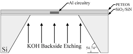
Fig. 1. Cross-sectional schematic of the fabrication process for the backside-etched microheaters (BE method).
bulk micromachining (hereafter termed the “column-release method”). The former was used to generate preliminary cell culture results, while the latter demonstrates a means through which flat, closely spaced microheated regions may be realized.
A. BE Method
Frequently, backside etching techniques are used to produce thermally isolated structures because of the low number of fabrication steps involved. Double-side alignment, however, is needed for the bulk backside etching in this process, which decreases the precision of heater element placement within the membrane. Moreover, sloped sidewalls (54.74 ) from anisotropic etching limit the proximity of heater elements to no less than , where is the wafer thickness.
Fabrication begins with a 6-inch, single-side polished, p-type (100) silicon wafer. A silicon oxide/nitride composite layer (300 /1500 ) is first deposited as an etch stop via thermal oxidation and low-pressure chemical vapor deposition (LPCVD). Next, aluminum is sputtered to a thickness of 5000 and chemically etched beneath a mask into the desired circuit pattern. Then, plasma-enhanced tetraethoxysilane (PETEOS; 1 -thick) is deposited, serving as a passivation layer, and is patterned through a second mask by reactive ion etching (RIE). Finally, a third mask is aligned on the wafer backside and KOH (35 wt%) is used to etch the wafer anisotropically for approximately 15 hr at 75 , leaving behind the membrane containing the heater [see Fig. 1]. The wafer was then diced partially with anisotropically etched V-grooves that partition the individual devices for straightforward separation; mechan-ical dicing significantly increases the likelihood of membrane fracture.
B. Column-Release Method
Currently, there are many techniques available to pro-duce closely spaced, thermally isolated heater elements (e.g., [17]–[20]), however the membranes can be structurally un-stable, usually incapable of containing complex geometric heater patterns, provide limited thermal isolation, and contain sharp topographical features. The following method was con-ceptualized in order to sidestep these potential shortcomings.
The process begins with a 6-inch, 675 -thick, single-side polished, p-type (100) silicon wafer. In the first step, a high-temperature furnace is used to grow a thermal oxide layer (300 ), upon which a 1500 -thick silicon nitride (SiN) film is deposited using LPCVD. This composite layer serves as the
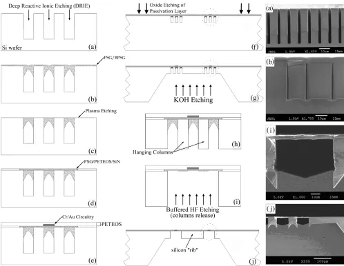
Fig. 2. Cross-sectional schematic of the fabrication steps for the column-release method and corresponding scanning electron micrographs for four of the fabrication stages (a, b, i, and j). Note that the dotted circles indicate the locations of the “zoomed-in” views.
Importantly, the multilayers of the membrane were thermally stress balanced during fabrication so as to reduce residual stress and prevent membrane cracking. Between each heater element are silicon “ribs” [see Fig. 2(j)] that provide additional struc-tural support and act as heat sinks to draw conducted heat away from the film surface. Note that the DRIE trench depth can be adjusted to control the heat-sinking capacity and accommodate larger temperature fluxes.
C. Final Devices
Microheated substrates were packaged by gluing them to a printed circuit board (PCB), wire bonding the contact sites to the PCB pads, and soldering in leads. A 35-mm polystyrene Petri dish (BD Falcon™) with a precut, 1.5 cm-wide hole was then attached to the top of the device with silicone adhesive (Selleys) and placed in a 70 oven for 10 min to cure. Consequently, the only surfaces contacting the culture medium during cell ex-periments were the Petri dish, silicone adhesive, and surface of the heater.
Preliminary cell studies were conducted on microheaters fab-ricated by the first protocol described; these membranes only contained a single heating element. An additional set of micro-heaters were created with the same fabrication procedure, but
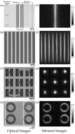
instead, five sensor elements one-third the width of the heater element were incorporated into the membrane and surrounding passivation layer to act as independent electrical resistance ther-mometers [see Fig. 3(a)]. Three heater configurations were pre-pared using the column-release method detailed above: a par-allel arrangement [see Fig. 3(b)], a nodal array [see Fig. 3(c)], and circular heaters [see Fig. 3(d)]. Infrared (IR) images (see Section III), illustrating the localized heating from the micro-heaters in Fig. 3(a)–(d), are shown in Fig. 3(e)–(h).
III. CHARACTERIZATION
A. Electrothermal Behavior
Fig. 3. Optical (a–d) and IR (e–h) micrographs of the top surfaces of (a) a heater with five sensor elements, (b) a parallel arrangement, (c) a nodal array, and (d) circular heaters. All experiments were conducted in air. A linear grayscale bar denotes the corresponding temperatures estimated from the R-T curves for each device. Note that the range of heating temperatures used for the IR microscopy experiments was much higher so that images with higher contrast could be acquired. The temperatures still dropped to ambient near the membrane edges at these high temperatures; the fact that these experiments were conducted in air should be considered, however.
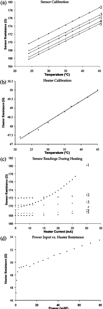
The data was fit using least-squares linear regression [see Fig. 4(a) and (b)]. It was assumed that the sample current used to measure the circuit’s resistance was small enough to avoid error from Joule heating. Calibrations performed in air were used during IR observation—discussed in Section III-B—while
Fig. 4. Calibration plots for (a) five sensor elements and (b) the heating element of a microheater that was fabricated by the BE method; (c) sensor resistance versus microheater current for the five sensor elements taken during Joule heating of the microheater; (d) input power versus heater resistance showing the large fluctuation in temperature for a small initial power input.
wire bonds were considered negligible, given that more than 98% of the circuit resistance was contained within the micro-heated region. As seen in Fig. 4(c), only “sensor 1,” embedded within the membrane, responded to the increase in heat, which demonstrates the degree of thermal isolation provided by the membrane. A very minimal amount of power was required to increase the heater temperature initially, and beyond that point the relationship was almost linear [see Fig. 4(d)].
Although we found the precision adequate for our purposes, it is worth noting that this could be improved further if necessary, as described below. The resistance of a wire is given by the following relation:
(1)
where is the temperature-dependent resistivity, is the length of the heater, and is the cross-sectional area. In order to improve the temperature accuracy of the heaters, the resistance of the heating element should be increased. Increasing and/or decreasing can achieve this. The electron mean free path for Au and Al is – at room temperature [21]–[23], and the maximum resolution of lithography used to etch the heater patterns is approximately 0.8 . Thus, using the current fab-rication methods, the practical dimensional limits of the heater cross-section are 1.0 0.1 . The maximum theoretical cir-cuit resistance would approach 2.5 for Au and Al heaters of these dimensions.
At a fixed voltage, the heater current will drift until equilib-rium is reached between the heater and its surroundings. Hence, to operate precisely in constant-temperature mode, some form of electronic feedback is needed to maintain a constant resis-tance. This can be accomplished by incorporating the heater into a Wheatstone bridge, setting the voltage, and having an op-amp maintain a balanced bridge [24]. In these preliminary experi-ments, the voltage was adjusted manually to sustain a relatively constant heater temperature .
B. Infrared Microscopy
At any temperature, a perfect emitter of radiation of all wave-lengths is considered a black body. Planck’s law relates the spec-tral emissive power of a black body to its temperature through the following:
(2)
where is the wavelength in , is absolute temperature, and
and are
the first and second radiation constants, respectively. Real ma-terials are not black bodies, but within narrow wavelength and temperature ranges can be considered “grey bodies” wherein the above equation holds true if the emissivity value of a material is considered.
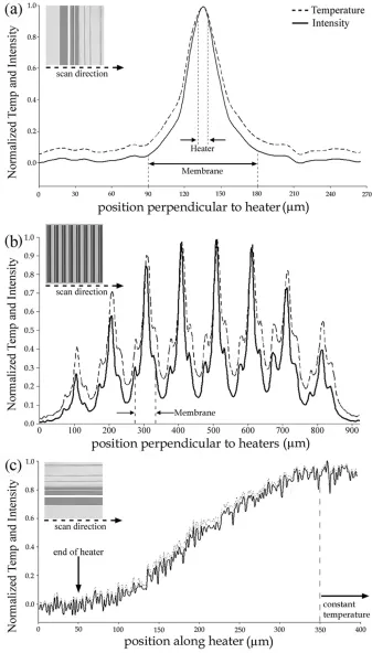
Fig. 5. Infrared microscopy linescans showing normalized intensity and calculated temperature values (a) perpendicular to the heating element of a BE-method microheater, (b) perpendicular to the heating elements of a parallel array, and (c) along the length of a heating element from a BE-method microheater.
normalized values of intensity and temperature vs. position were plotted to show a general trend, and the maximum was es-timated from an R-T curve. Furthermore, IR experiments were conducted in air because water strongly absorbs IR radiation.
par-allel array, and baseline values near the center heater were ele-vated [see Fig. 5(b)]. As illustrated in Fig. 5(c), the temperature along the axis of the heater dropped near the end, yet could be considered constant along 88% of the heating element length.
C. Finite Element Modeling
To help optimize heater design and to validate the IR data and sensor readings independently, two-dimensional (2-D) steady-state heat conduction and free-convection flow simulations were performed with the finite element model program ANSYS 7.0. Material property values found in the literature [28] were used. The simulation confirmed our experimental measurements, which showed that if the microheater is run at a low temperature (e.g., up to above ambient) the temperature drops rapidly to ambient temperature at or near the membrane’s edge. This is due to the heat-sinking capacity of the supporting silicon substrate. Accordingly, it can be expected that, when used at low temperatures, our microheaters have no significant thermal effect on cells grown away from the membrane. This allows us to impart distinct temperature differences between cells grown on the membrane and those grown at any other location. It is expected that the presence of a mass of cells will influence the proximal thermal fields, thus simulations that incorporate such inhomogeneities will be needed to carefully define the temper-ature state throughout the cell structure.
[image:7.594.305.552.64.440.2]In addition to growing cells under different thermal condi-tions, there was also an interest to exploit convection currents to position cells on the microheater substrate. To determine the effective range for gathering cells and patterning them on the heater membrane, a free convection simulation was run at various microheater temperatures in a water environment [see Fig. 6]. The model showed that unattached cells resting more than 200 from the membrane could be moved toward the heater at a rate of approximately 2–15 using tem-peratures ranging from 15–30 above ambient. This result was confirmed experimentally using time-lapse videos of cell movement (see Section IV).
D. Surface Topography
A profilometer (KLA-Tencor P-10) was used to evaluate the surface topography of each of the five different microheater membrane regions. Maximum slope values (rise/run) of the sur-face features were determined to be 0.94, 0.22, 0.41, and 0.45 for the BE (with and without sensors), parallel, nodal array, and circular heater configurations, respectively. Profilometer scans across the entire membrane at the heater midpoint also eluci-dated the maximum amount of residual stress remaining in the heater structures due to thermal mismatching during fabrication. An insignificant curvature, , was observed in every case other than the parallel configuration. The large membrane width (800 ), coupled with the high aspect ratios of the support struc-tures below, could explain the small warpage observed in the parallel configuration. If then can be approx-imated by
(3)
Fig. 6. ANSYS 2-D cross-sectional simulations of steady-state (a) heat conduction through water above the surface of a BE-method microheater when operating at 42 Cand (b) free convection velocities within the culture medium above the same type of microheater operating at 25 Cabove room temperature. Independent time-lapse video showed cell velocities up to 17m=sat this temperature. Plots were graphically formatted to improve clarity.
where is radius of curvature, is the width of the membrane (chord), and is the chordal deviation (0.25 maximum height of warpage) [29]. Using (3), was found to be 2520 for the parallet configuration, suggesting that the thermal-stress bal-ancing was effective.
IV. CELLCULTURE
ducted. For cell heating experiments, substrates were placed back into an incubator for 2 h to allow for adequate attachment. In contrast, cell patterning involved the movement of cells by free convection, hence attachment would have been a hindrance and experiments were run within 5min of cell deposition. Fol-lowing attachment, differentiation of C17.2 cells was induced by gently removing the serum-free DMEM and replacing it with an N2-supplement/DMEM-F12 solution (1:1; Invitrogen).
V. RESULTS ANDDISCUSSION
A. Heating Attached Neurons
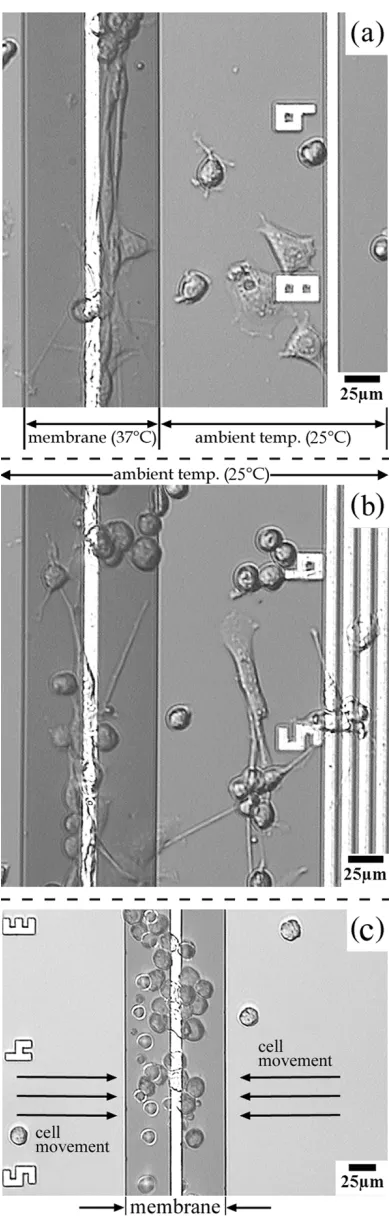
Most mammalian cells seem to be preprogrammed to func-tion optimally around 37 and will alter their physiological behavior to maintain this temperature state, from migration along thermal gradients to the release of heat-shock proteins [31]. Therefore, there are two approaches to heating cells: 1) dropping the ambient temperature below 37 and operating the heater at 37 (attracting mode) or 2) maintaining a phys-iological ambient temperature and operating the heater above 37 (repelling mode). The former was chosen to demonstrate microscale temperature-based control over cell growth. In this scenario, cells grown within the microheated region are given a metabolic advantage over their neighbors (developing at a much lower temperature). It has been shown, for example, that the metabolic activity in neurons cultured at 22 is slowed significantly, thus delaying differentiation and extending the viability of the cells by several days [1]. In Fig. 7(a), cells were in culture for 18 h at 25 while the microheater was kept at approximately 37 . Cells grown on the membrane differentiated and extended long processes while neurons developing at 25 showed subtle morphological changes. A set of control studies were conducted by culturing neurons at both room temperature and 37 for more than 24 hr on the microheater substrates without supplying power to the heaters [see Fig. 7(b)]. Results showed randomly oriented outgrowth, which demonstrates a lack of appreciable topographical or chemical influence from the substrate’s surface on cellular development. While general observations of characteristic out-growth were made, a quantitative analysis of cell morphology was not performed in this study, i.e., calculations of zero-, first-, and second-order moments for each cell. For further details, refer to [32] for a proposed approach to estimating extension and dispersion based upon cell moments.
[image:8.594.329.524.60.670.2]The ability to switch an environmental cue off and on, and/or vary the intensityin situ, has exciting potential for un-derstanding cell development and behavior. In this manner, neural differentiation and outgrowth can be potentially coordi-nated and locally regulated to influence the polarity of specific
Fig. 7. Optical micrographs of a BE substrate illustrating (a) spatially selective acceleration of neural outgrowth by heating cells grown on the microheated membrane, (b) control experiment demonstrating random growth in the absence of thermal gradients (spherical cells are unattached and undifferentiated), and (c) collecting and patterning unattached neurons using free-convection currents.
overall cellular response when neural structures such as the growthcone, soma, dendrites, and axon are heated indepen-dently. It is unknown, for instance, which portions of a neuron are able to sense a temperature variation and initiate the ap-propriate migration or outgrowth response, or if the response is altered after the cell has developed fully. An understanding of this may provide insight into differences in mechanisms of signal transduction between developing and fully matured cells.
B. Patterning Neurons Using Convection
During the initial stages of attachment, weak cell-substrate in-teraction forces are formed as the cells approach the surface. The heater was turned on after the undifferentiated neurons settled to the surface but prior to the establishment of strong attachment forces. On account of the small volume of fluid being heated, convection currents reached a steady state within seconds of powering the microheater, allowing for the precise timing of cell movement. Further, adjusting the heater temperature altered the resulting velocity gradient near the surface. An example of cell patterning can be seen in Fig. 7(c), in which a room-temperature cell suspension with a density of was pipetted onto the substrate and after 5 min the heater was powered and kept at 45 for 15 min. The neurons appeared to slide across the surface toward the heater or, occasionally, looked as though they were rolling. It should be noted that because the cells were probably at a lower temperature than the heater, and because they were heated for a relatively short period of time, there were no signs of cellular damage and normal neuronal growth ensued after patterning in this manner.
Convection experiments were straightforward with the im-portant parameters being heater temperature and cell density. Using this method, it is possible to force cells to aggregate lo-cally, or by lowering the cell density, collect cells in a single-file fashion. One significant advantage of being able to aggregate cells locally on the microscale is explained below. In high-density culture conditions, cells have been shown to ignore environmental cues in favor of biochemical vectors emanating from surrounding cells (e.g., growth factors). Thus, the cell density is often lowered during experimentation in order to study the effects of certain cues independently, but for the cells to survive, their medium may need to be supplemented with that of a high-density culture. Therefore, microheated substrates can be used to create smaller regions of high cell confluence, and hence improve culture conditions surrounding a low-confluence area wherein the effects of cell-cell interac-tions are minimized and the influence of other environmental cues can be studied.
The importance of patterned and oriented growth in tissue en-gineering is not limited to neurons, however. Many tissues rely on a specific cellular alignment and orientation to function prop-erly. For example, endothelial cells, which line the interior of blood vessels, are oriented so that their major axis is perpendic-ular to the direction of blood flow. Moreover, skeletal muscle contains cells that are highly oriented and packed tightly. These types of requirements give rise to difficulties when engineering useful tissues.
VI. CONCLUSION
Two types of thermally isolated microheated substrates were fabricated and characterized. The microheaters met our criteria of having smooth closed-membrane surfaces, sufficient thermal isolation on the microscale, and allowing for arbitrarily pat-terned heating regions. Experimental measurements and simula-tions confirmed that the microheater substrates were sufficiently precise and accurate for our experimental purposes. Using our devices, it was demonstrated that microheated environments can be used to 1) pattern cells using free convection and 2) accel-erate neural development selectively within heated regions. We believe that being able to control (i.e., switch on and off and vary intensity) cellular cues on the microscale will lead to a greater understanding of cellular development and may eventually lead to practical methods for patterning and integrating cells into mi-croelectronic devices.
To improve the accuracy of the heater element, and to better define the thermal profile along the width of the membrane and surrounding substrate, new microheaters are being fabricated that have a sensor less than 2 from the heater and two addi-tional sensors within the membrane. Furthermore, these sensor elements will have a much smaller cross-section to increase their nominal resistance.
Recently, a microheater array was used in conjunction with a thermo-responsive polymer coating to create patterned adhe-sion sites for cell growth [33]. Though the microheaters were not thermally isolated and the patterned region was approxi-mately 1mm, the study demonstrates the possibility of using microheated regions to control the timing of attachment and to form cell patterns at the microscale. Hence, the concept of using a thermally isolated microheated region as a develop-mental switch can be incorporated into many existing methods of locally manipulating cellular development.
REFERENCES
[1] J. C. Magee and G. G. Schofield, “Room-temperature culture extends the useful life of adult neurons for voltage-clamp experiments,”J. Neuro. Meth., vol. 38, pp. 201–208, 1991.
[2] A. Higazi, D. Kniss, J. Manuppello, E. S. Barnathan, and D. B. Cines, “Thermotaxis of human trophoblastic cells,”Placenta, vol. 17, pp. 683–687, 1996.
[3] R. Wolf, J. Niemuth, and H. Sauer, “Thermotaxis and protoplasmic os-cillations in physarum plasmodia analyzed in a novel device generating stable linear temperature gradients,”Protoplasm, vol. 197, pp. 121–131, 1997.
[4] A. Bahat, I. Tur-Kaspa, A. Gakamsky, L. C. Giojalas, H. Breitbart, and M. Eisenbach, “Thermotaxis of mammalian sperm cells: A potential navigation mechanism in the female genital tract,”Nature Med., vol. 9, pp. 149–150, 2003.
[5] P. Clark, P. Connolly, A. Curtis, J. Dow, and C. Wilkinson, “Cell guidance by ultrafine topography in vitro,”J. Cell Sci., vol. 99, pp. 73–77, 1991. [6] A. Curtis and M. Varde, “Control of cell behavior: Topographical
fac-tors,”J Natl. Cancer Inst., vol. 33, pp. 15–26, 1994.
[7] N. M. Dowell-Mesfin, M.-A. Abdul-Karim, A. M. P. Turner, S. Schanz, H. G. Craighead, B. Roysam, J. N. Turner, and W. Shain, “Topograph-ically modified surfaces affect orientation and growth of hippocampal neurons,”J. Neur. Eng., vol. 1, pp. 78–90, 2004.
[8] A. Curtis and C. Wilkinson, “Nanotechniques and approaches in biotechnology,”Trends Biotech., vol. 19, pp. 97–101, 2001.
[9] C. S. Chen, M. Mrksich, S. Huang, G. M. Whitesides, and D. E. In-gber, “Geometric control of cell life and death,”Science, vol. 276, pp. 1425–1428, 1997.
Cell Biol., vol. 101, pp. 2023–2027, 1985.
[16] K. Y. Nishimura, R. R. Isseroff, and R. Nuccitelli, “Human keratinocytes migrate to the negative pole in direct current fields comparable to those measured in mammalian wounds,”J. Cell Sci., vol. 109, pp. 199–207, 1996.
[17] A. D. Oliver and K. D. Wise, “A 1024-element bulk-micromachined thermopile infrared imaging array,”Sens. Actuators A, Phys., vol. 73, pp. 222–231, 1999.
[18] S. Wu, Q. Lin, Y. Yin, and Y.-C. Tai, “MEMS flow sensors for nano-fluidic applications,”Sens. Act. A, vol. 89, pp. 152–158, 2001. [19] I. Simon, N. Barsan, M. Bauer, and U. Weimar, “Micromachined metal
oxide gas sensors: Opportunities to improve sensor performance,”Sens. Actuators B, Chem., vol. 73, pp. 1–26, 2001.
[20] K. S. Breuer, R. Bayt, and A. Nayaar, “Micromachined shear and tem-perature sensors,” inProc. 4th ASME Microfluids Symp., 1999. [21] D. R. Penn, “Electron mean-free-path calculations using a model
dielec-tric function,”Phys. Rev. B, vol. 35, pp. 482–486, 1987.
[22] S. Tanuma, C. J. Powell, and D. R. Penn, “Calculations of electron in-elastic mean free paths. II. data for 27 elements over the 50–2000 eV range,”Surf. Int. Anal., vol. 17, pp. 911–926, 1991.
[23] J. I. Avila, A. L. Cabrera, J. Baier, I. K. Schuller, and I. V. Roshchin, “Measuring thicknesses of plasma oxide Al thin films by resistivity,” in CLACSA, 2003.
[24] J. G. Webster,Medical Instrumentation: Application and Design. New York: Wiley, 1998, pp. 356–357.
[25] A. D. Trigg, “Temperature mapping of IC’s and MEMS devices using an infrared microscope,” inProc. Therminic Conference, Budapest, Hun-gary, 2000.
[26] , “A combined infrared/visible photoemission microscope,” in Proc. 25th Inter. Symp. for Test and Fail Analy (ISTFA), 1999, pp. 457–464.
[27] , “Application of a mercury cadmium telluride focal plane array to semiconductor device manufacturing and reliability,”SPIE, vol. 3898, pp. 312–322, 1999.
[28] J. Puigcorbe, D. Vogel, B. Michel, A. Vila, I. Gracia, C. Cane, and J. R. Morante, “Thermal and mechanical analysis of micromachined gas sensors,”J. Micromech. Microeng., vol. 13, pp. 548–556, 2003. [29] D. Malacara,Optical Shop Testing, 2nd ed. New York: Wiley, 1992,
pp. 459–463.
[30] E. Y. Snyder, D. L. Deitcher, C. Walsh, S. Arnold-Aldea, E. A. Hartwieg, and C. L. Cepko, “Multipotent neural cell lines can engraft and partic-ipate in development of mouse cerebellum,”Cell, vol. 68, pp. 33–51, 1992.
[31] S. Lindquist and E. A. Craig, “The heat-shock proteins,”Annu. Rev. Genet., vol. 22, pp. 631–677, 1988.
[32] G. A. Dunn and A. F. Brown, “Quantifying cellular shape using moment invariants,” inBiological Motion, W. Alt and G. Hoffman, Eds. Berlin, Germany: Springer, 1990, pp. 254–268.
[33] X. Cheng, Y. Wang, Y. Hanein, K. F. Böhringer, and B. D. Ratner, “Novel cell patterning using microheater controlled thermoresponsive plasma films,” J. Biomed. Mater. Res., to be published.
Wenmiao Shu received the B.Eng. degree in polymer materials from Dalian University of Tech-nology, China, in 1998 and the M.Sc. degree in advanced materials for micro- and nano-systems from the Singapore-MIT Alliance in 2002. From 2002 to 2003, he was a Senior Research Officer in the Institute of Materials Research and Engineering (IMRE), Singapore. Currently, he is pursuing the Ph.D. degree in bio-nanotechnology from Cam-bridge University, U.K.
reflection microscopy, and vascular and soft tissue mechanics.
Qing X. Zhang received the Ph.D. degree in mi-croelectronics from Tsinghua University, China, in 1997.
Currently, he is a Senior Research Engineer at the Institute of Microelectronics (IME) in Singapore. His major interests are MEMS design, simulation, process development, and process integration.
Minghui H. Liureceived the B.S. degree in chem-istry from Fudan University, China, in 2000 and the M.S. degree in materials science from National Uni-versity of Singapore in December 2004.
She is currently working as a Research Officer at the Institute of Materials Research and Engineering (IMRE), Singapore. Her primary research interest is nanoassembly via electrochemical methods.
Alastair Trigg (M’97) received the Ph.D. degree from London University, London, U.K., in 1978.
He is currently a Member of Technical Staff at the Institute of Microelectronics (IME), Singapore, spe-cializing in failure analysis and reliability.
Yuexia Mareceived the M.D. degree from Chinese Medical Science University, China, in 1984.
S. Mark Spearingreceived the Ph.D. degree from Cambridge University Engineering Department in 1990.
He is a Professor of Engineering Materials at the University of Southampton in the United Kingdom, having been Professor of Aeronautics and Astro-nautics at the Massachusetts Institute of Technology (MIT), Cambridge, where he served from 1994 to 2004. His technical interests include materials characterization and structural analysis and design of MEMS, development of wafer bonding-tech-nologies and other processes, micro-electronic and MEMS packaging, and advanced composites. Since 1995, he has been responsible for materials, structural design, and packaging tasks of the MIT MicroEngine, MicroRocket, Micro-Chemical Power and MicroHydraulic Transducer projects as well as conducting cross-cutting underpinning technology development.
Dr. Spearing is an Editor of the JOURNAL OFMICROELECTROMECHANICAL
SYSTEMS.
Shu Wangreceived the Ph.D. degree from Gothen-burg University, Sweden.
He is currently an Associate Professor at Depart-ment of Biological Sciences, National University of Singapore and a group leader in gene de-livery/therapy in the Institute of Bioengineering and Nanotechnology (IBN), Singapore.
Hung-Jue Suereceived the S.B. degree in chemical engineering at Chung-Yuan University, Taiwan, and the S.M., S.M., and Ph.D. degrees in materials science, mechanical engineering, and macromolec-ular science and engineering from the University of Michigan, Ann Arbor, in 1981, 1985, 1987, and 1988, respectively.
He is currently the Director of the Polymer Tech-nology Center and a Full Professor at the Mechan-ical Engineering Department, Texas A&M Univer-sity. His research interests include structure-property relationship in polymers and nanocomposites, synthesis and characterization of functional nanoparticles for optoelectronic applications, and surface deforma-tion and damage of polymers.
Peter M. Moranreceived the Ph.D. degree in solid mechanics from Brown University, Providence, RI.
![Fig. 6]. The model showed that unattached cells resting more](https://thumb-us.123doks.com/thumbv2/123dok_us/8513474.350812/7.594.305.552.64.440/fig-model-showed-unattached-cells-resting.webp)