This is a repository copy of
Double crystal x-ray diffraction simulations of diffusion in
semiconductor microstructures
.
White Rose Research Online URL for this paper:
http://eprints.whiterose.ac.uk/1678/
Article:
Fatah, J.M., Harrison, P., Stirner, T. et al. (2 more authors) (1998) Double crystal x-ray
diffraction simulations of diffusion in semiconductor microstructures. Journal of Applied
Physics, 83 (8). pp. 4037-4041. ISSN 1089-7550
https://doi.org/10.1063/1.367159
[email protected] https://eprints.whiterose.ac.uk/
Reuse
See Attached
Takedown
If you consider content in White Rose Research Online to be in breach of UK law, please notify us by
Double crystal x-ray diffraction simulations of diffusion in semiconductor
microstructures
J. M. Fatah, P. Harrison,a)T. Stirner,b)J. H. C. Hogg, and W. E. Hagston
Department of Physics, University of Hull, Hull HU6 7RX, United Kingdom
~Received 17 July 1997; accepted for publication 23 December 1997!
Diffusion in group IV, III-V and II-VI semiconductors is an interesting problem not only from a fundamental physics viewpoint but also in practical terms, since it could determine the useful lifetime of a device. Any attempt to control the amount of diffusion in a semiconductor device, whether it be a quantum well structure or not, requires an accurate determination of the diffusion coefficient. The present theoretical study shows that this could be achieved via x-ray diffraction studies in quantum well structures. It is demonstrated that the rocking curves of single quantum wells are not sensitive to diffusion. However the intensity of the first order satellite, which is characteristic of superlattice rocking curves, is strongly dependent upon diffusion and it is proposed that this technique could be used to measure the diffusion coefficient D. © 1998 American
Institute of Physics.@S0021-8979~98!01608-9#
I. INTRODUCTION
Diffusion has been studied in bulk semiconductors for many years1. The use of diffusion in the post-growth fine tuning of devices based on semiconductor microstructures has become increasingly important.2,3 Diffusion could also play an important role in the viability of devices from the viewpoint of their operating properties. In particular diffu-sion of an alloy component such as Al in GaAs–Ga12xAlxAs, Mn in CdTe–Cd12xMnxTe or S in
ZnSe–ZnSxSe12xwill affect the optoelectronic properties of
the device and could ultimately render the device useless. Hence from the viewpoint of both device fabrication and device stability quantitative knowledge of the amount of dif-fusion is essential if they are to be optimized and controlled, respectively.
Certain probes of diffusion have already been suggested, such as the excitonic optical properties of quantum well structures4 and, for the diffusion of a magnetic ion ~e.g., Mn21), the polaronic properties.5While the polaronic
prop-erties in a magnetic field could offer an accurate measure of the diffusion coefficient of a magnetic ion, they are obvi-ously limited to diluted magnetic semiconductors. Similarly, although the excitonic optical properties of nonmagnetic ma-terials could be employed successfully to investigate diffu-sion, they would probably need to be used in conjunction with another technique, such as x-ray diffraction, in order to reduce any uncertainties in quantum well widths, etc.
In the present theoretical work it will be demonstrated that semiconductor quantum well structures offer a unique environment for probing diffusion. In particular it is shown that computer simulations of double crystal x-ray diffraction ~DCXRD!curves for annealed multiple-quantum well struc-tures, in conjunction with the corresponding experimental
data, can provide an accurate measure of the diffusion con-stant of an alloy constituent in all of the technologically sig-nificant group IV, III-V and II-VI semiconductors.
II. COMPUTER SIMULATION
To interpret the rocking curves resulting from x-ray dif-fraction studies of crystals and to obtain accurate values for various structural parameters~such as the alloy concentration
x, the degree of lattice relaxation, etc.! it is important to carry out a profile simulation.6This profiling can be done by simulating the diffraction of x rays from crystals using the dynamical x-ray diffraction theory, reviews of which are given in Refs. 7 and 8. The problem is to solve Maxwell’s equations in a medium which has a complex, triply periodic electric susceptibility x. In the x-ray case only two waves with appreciable amplitudes are normally allowed to exist within the crystal. These two, the incident and diffracted waves, are described by the wave vectors K0 and Kh, and
are connected to the reciprocal lattice vector h by the Laue equation
K01Kh5h. ~1!
The solution, Equation ~2!, defines the dispersion surface, which is the locus of the end points of the allowable wave vectors inside the crystal.
a0ah5
1 4C
2k2x
hxh¯. ~2!
Here C is the polarization factor, k5uK0u5uKhu51/l ~at the
wavelengthl) anda0 andah are given by
a05
1
2k@K0.K02k
2
~11x0!#
ah5
1
2k@Kh.Kh2k
2~1
1x0!#.
The total wavefield Dtot is related to the amplitudes of the
direct and diffracted waves, D0 and Dh, by
a!Present address: Dept. of Electron. and Electron. Eng., University of Leeds, Leeds LS2 9JT, U.K.
b!Electronic mail: [email protected]
4037
Dtot5
(
j51 2@D0 j exp~22piK0 j.r!
1Dh jexp~22piKh j.r!#.
The amplitude ratio X
8
(5Dh/D0(z)) is given by therela-tion
X
8
5 2a0 kCxh¯5kCxh
2ah
.
The relative strengths of the direct and diffracted beams emerging from the perfect crystal thus depend ona0andah,
which in turn depend on the deviation DQ of the incident beam from the exact Bragg angle. Thus as the crystal is rotated, the diffracted intensity changes, giving the rocking curve its finite width.
The generalized diffraction theory, developed by Takagi9and Taupin,10can be used to describe the passage of x-rays through a crystal with any type of lattice distortion. In the two-beam approximation the wavefield inside the crystal can be described by two coupled first order partial differen-tial equations expressed along the depth z into the crystal
il
pg0 ]D0
]z 5x0D01Cxh¯Dh, ~3!
il
pgh ]Dh
]z 5~x02ah!Dh1CxhD0, ~4!
where xh is related to the structure factor Fh, the electron
radius reand the unit cell volume V by
xh5l
2r e pV Fh.
g0 andgh are the direction cosines of the incident and
re-flected beams relative to the inward surface normal. The pa-rameter ah, which represents the deviation of the incident
wave from the exact Bragg condition, is given by
ah~v!522l
dDQh cos~ QB!,
where DQh is the local deviation from the exact Bragg angle, taking lattice strains into account,QB is the local ex-act Bragg angle and d is the interplane spacing.
Equations~3!and~4!can now be combined, by defining an amplitude ratio X
85
Dh/D0(z), and integrated.11We thusobtain the amplitude ratio X(Z)
X~Z,v!5X
8
~z,v!S1i~BX8
~z,v!1E!tan~DS@z2Z# ! S2i~AX8
~z,v!1B!tan~DS@z2Z# ! ,~5!
where the variable z is the depth above the depth Z at which the amplitude ratio is the known value X
8
. In Equation~5! we use the parameters11A5ughug
0 xh¯
B51
2
FS
12ughu g0
D
x02ah~v!
G
D52 p
lughu
E5xh
and
S5
A
B22AE.To calculate the diffraction profile we need to establish a starting amplitude ratio~chosen as zero deep inside the crys-tal! and progress up through the crystal layers, and use the amplitude ratio at the top of one layer as the start value for the bottom of the next. This procedure is then repeated for each step in the crystal rotation angle v.
In the present work interest is focused upon the Cu Ka
1
004 rocking curve. To be definite, a quantum well stack which was commensurate with, and grown upon, a 001 InSb substrate with a 1000 Å CdTe buffer layer was employed in the model calculations.
For the purposes of the simulation of rocking curves, quantum well structures can be described completely in terms of alternating layers of material. In the present case Cd12xMnxTe layers were assumed, with differing alloy
con-centrations x. When one of the alloy constituents has dif-fused ~i.e., Mn!, a more complex variation of x along the growth (z) axis occurs. In order to model the latter it is assumed, for the purpose of illustration, that the diffusion coefficient D does not vary with the alloy concentration x. This leads to Fick’s second law in one dimension,
]x
]t5
] ]zD
S
]x
]z
D
, ~6!which has been described in detail in an earlier publication.4 Various standard solutions to the linear case of Fick’s second law do exist,12,13depending on the initial distribution of the diffusing substance. For the following calculations, Crank’s12solution to the diffusion equation for a source with an extended initial distribution has been employed. Using xo
for the initial concentration of the diffusing substance, Crank’s equation reads
x5 xo
2 erfc
S
z
2
A
DtD
, ~7!where erfc denotes the complementary error function. The supposed linearity of Fick’s second law, i.e., the constancy of the diffusion coefficient D, now allows a linear superpo-sition of the separate solutions to the diffusion equations at any given time t.
It should also be pointed out that the following calcula-tions are not microscopic in the sense that there is no refer-ence to impurity atoms or lattice defects, such as interstitials or vacancies ~which can enhance diffusion processes dra-matically!. For such a calculation, which takes impurities and lattice defects into account, a diffusion Monte Carlo
analysis would be necessary. However, the macroscopic model employed is of proven utility for abstracting informa-tion from experimental data.14
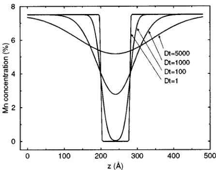
Figure 1 shows diffusion profiles for a single CdTe well of width 80 Å, surrounded by 200 Å Cd0.925Mn0.075Te
barri-ers, in which the diffusion is due entirely to a post-growth anneal. As a linear diffusion process has been assumed the curves are universal, i.e., the diffusion coefficient and the time are interchangeable. Hence the separate graphs are la-belled with the corresponding product of diffusion coeffi-cient D and time t ~in units of Å2). For example, if we assume for the graph with the largest amount of diffusion a diffusion coefficient of D50.1 Å2/s we obtain, by using the
Dt value of 5000 Å2, a corresponding annealling time of t
550 000 s'14 h.
III. RESULTS AND DISCUSSION
A. Diffusion of single quantum wells
Figure 2 shows the simulated rocking curves for the single quantum well structures of Fig. 1. Note that for the purpose of clarification the curves have been scaled. It is clear that the central~substrate!peak dominates and, at first
sight, the curves are virtually identical, even though the quantum wells themselves are significantly different. Subtle differences between the curves do exist in the peak centred around 700–800 arcsec, but they are far too small to be detectable with any reliability by experiment. In summary, single quantum wells are of limited utility from the view-point of DCXRD studies for the investigation of diffusion.
B. Diffusion of superlattices
[image:4.612.64.287.49.225.2]It is envisaged that superlattices could be a more sensi-tive measure of diffusion, since the additional periodicity of the superlattice unit cell leads to a strong feature ~i.e., the superlattice satellites!on the rocking curve, which is charac-teristic of the exact form of the structure. In particular the angular separation of the first order satellite from the sub-strate peak is a measure of the superlattice period. Further-more, the height and width of the peak give an indication of the number of repeats and uniformity of the periodicity.
[image:4.612.324.551.52.212.2]Figure 3 displays the simulated rocking curve ~of the sample described in Fig. 4 below! with no diffusion. It is clear from this figure that the first order satellite peaks are an order of magnitude larger than the second order ones. From an experimental viewpoint, this means that it is much more
[image:4.612.323.549.558.732.2]FIG. 1. Diffusion profiles for a single CdTe well of width 80 Å, surrounded by Cd0.925Mn0.075Te barriers, for various values of Dt~in Å2).
FIG. 2. Simulated Cu Ka1004 DCXRD rocking curves for the single
quan-tum wells of Fig. 1.
FIG. 3. Simulated Cu Ka1004 DCXRD rocking curve for 15380 Å CdTe
wells separated by 80 Å Cd0.925Mn0.075Te barriers with no diffusion.
FIG. 4. Diffusion profiles for the sample of Fig. 3 with varying values of Dt
[image:4.612.61.288.574.733.2]difficult to monitor accurately the changes in the second or-der satellites. Hence although the latter are sensitive to the well shape15we will focus our attention in the present paper on the first order satellites which can be more accurately monitored experimentally.
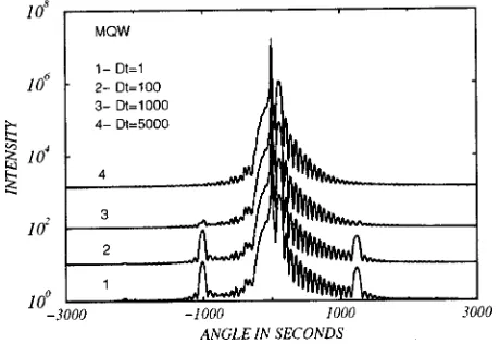
For comparison with the previous section, the superlat-tice was chosen to have 15 80 Å CdTe wells, separated by 80 Å Cd0.925Mn0.075Te barriers, with 200 Å outer barriers. Em-ploying the same Dt values as in Section III A, the manga-nese concentration x as a function of distance z along the growth direction is displayed in Fig. 4.
[image:5.612.319.554.51.228.2]The simulated rocking curves for the superlattices of Fig. 4 are shown in Fig. 5. Although the first order superlat-tice satellites are clearly visible in the bottom curve of Fig. 5 at angles of'21000
9
and112009
, for increasing amounts of diffusion these satellite peaks are eroded away, while the rest of the curves remain virtually unaltered. This could have been anticipated a priori since increasing amounts of diffu-sion in a superlattice would lead eventually to a uniform alloy~as shown in the Dt55000 Å2 curve of Fig. 4!, which would contain no superlattice periodicity and hence no su-perlattice satellites would be observed. The diffusion profiles displayed in Fig. 4 clearly represent intermediaries between the two extremes of a square well superlattice and an alloy. The intensity of both first order superlattice satellites are plotted as a function of Dt in Fig. 6. It can be seen that the intensities are a sensitive function of the amount of diffusion; in this case the peaks decrease by about a factor of 10 from the superlattice with effectively no diffusion~i.e., Dt51 Å2) to that with considerable diffusion ~i.e., Dt55000 Å2). As the annealling time in any post-growth process is easily mea-sured, then Fig. 6 demonstrates that DCXRD could be used to measure the diffusion coefficient D for any particular an-nealing temperature by repetitive measurements on the same sample at successively longer time intervals.Note that although attention has been focused upon the CdTe–Cd12xMnxTe system, the results are completely
gen-eral. The technique could be equally applied to Al diffusion in GaAs–Ga12xAlxAs or Ge in Si–Si12xGex strained layer
superlattices, by simply growing the appropriate multiple-quantum well structure and performing annealing and x-ray diffraction measurements. In fact, the effects desribed in this
section have recently been observed in an experimental x-ray diffraction study of thermally induced disordering in a ZnSSe–ZnSe superlattice system.16
C. Diffusion during growth
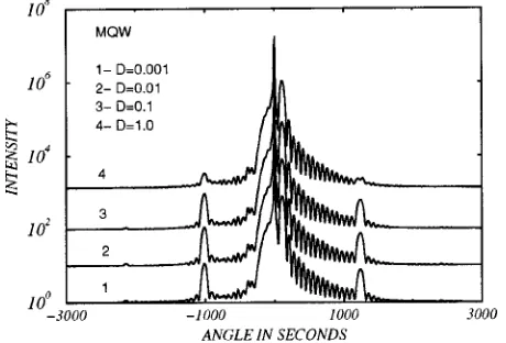
The conclusions of the previous section are based on the assumption that no diffusion occurs during growth of the superlattice. Depending on the diffusion coefficient ~which could be a strongly varying function of the growth tempera-ture!and the total growth time~which itself depends on the growth rate and the overall thickness of the superlattice stack! the amount of diffusion during growth could be sig-nificant.
Figure 7 shows the effect of such diffusion during the growth of the superlattice of Section III B, for various values of D ~in units of Å2/s!. There is no post-growth annealing, hence the last well to be grown exhibits virtually no diffu-sion, while the first well can exhibit significant diffusion. In these calculations the growth rate was chosen to have the typical value of 1.83 Å/s. The curves are no longer universal, hence the diffusion coefficient D has been chosen to
repre-FIG. 5. Simulated rocking curves for the superlattices of Fig. 4 with differ-ing amounts of diffusion (Dt in units of Å2).
FIG. 6. Peak intensity of the first order superlattice satellites of Fig. 5 as a function of the amount of diffusion Dt.
FIG. 7. Superlattice of Fig. 3 with diffusion during growth only (D in units of Å2/s!.
[image:5.612.60.290.53.211.2] [image:5.612.323.551.558.732.2]sent the extremes of hardly any diffusion (D50.001 Å2/s!to almost total destruction of the first well grown (D51 Å2/s!. Note that only curves for D50.1 and 1 Å2/s are shown for clarity. The diffusion time t for the first layer is now set as the growth time, i.e.,
t5total thickness of superlattice stackgrowth rate 51.83 Å/s2720 Å '25 min.
Clearly the diffusion time decreases to zero for the last layer in the stack and takes on intermediate values between these two limits for different layers. Figure 8 illustrates the dy-namical simulation of the x-ray rocking curves of the super-lattices of Fig. 7, together with those appropriate to D
50.01 and 0.001 Å2/s. As in Section III B, the rocking curves remain virtually unaltered except for the first order superlattice satellites at '21000
9
and112009
, which are dramatically reduced. This is not due specifically to a loss of superlattice periodicity, but to a reduction in the difference between well and barrier material, as the earliest grown wells tend towards alloys, as shown in Fig. 7.Figure 9 summarizes the changes in the satellite peak intensities for both left ('21000
9
) and right ('112009
) first order peak. Hence, the amount of diffusion occurring during growth can be deduced by comparison of the simula-tion of the experimentally measured rocking curve, with the simulation of the ideal ~i.e., undiffused! rocking curve. The growth conditions can then be adjusted accordingly to con-trol such processes.IV. CONCLUSION
It has been demonstrated that multiquantum well struc-tures offer an invaluable means of measuring the diffusion coefficient of any semiconductor. Simulations of DCXRD rocking curves cannot only be utilized to quantify the
diffu-sion occurring in post-growth annealling, but can also be used to determine the amount of diffusion occurring during growth of semiconductor heterostructures.
ACKNOWLEDGMENT
The authors would like to thank EPSRC ~U.K.! for fi-nancial support.
1D. Shaw, J. Cryst. Growth 86, 778~1988!.
2K. Meehan, P. Gavrilok, N. Holonyak, R. D. Burnham, and R. L. Thorn-ton, Appl. Phys. Lett. 46, 75~1985!.
3
K. P. Homewood, B. L. Weiss, and A. C. Wismayer, Semicond. Sci. Technol. 4, 472~1989!.
4P. Harrison, W. E. Hagston, and T. Stirner, Phys. Rev. B 47, 16 404
~1993!.
5T. Stirner, W. E. Hagston, P. Harrison, and J. P. Goodwin, J. Appl. Phys. 75, 3466 ~1994!; T. Stirner, P. Harrison, and W. E. Hagston, ibid. 77, 1314~1995!.
6J. H. C. Hogg, J. E. Nicholls, S. R. Jackson, W. E. Hagston, D. E. Ash-enford, B. Lunn, and S. Ali, Mater. Sci. Eng. B 16, 60~1993!. 7
B. W. Batterman and H. Cole, Rev. Mod. Phys. 36, 681~1964!. 8
Z. G. Pinsker, Dynamical Scattering of X-rays in Crystals~Springer, New York, 1978!.
9S. Takagi, Acta Crystallogr. 15, 1311~1962!; J. Phys. Soc. Jpn. 26, 1239
~1969!. 10
D. Taupin, Bull. Soc. Fr. Mineral. Cristallogr. 87, 469~1964!.
11P. F. Fewster, J. Appl. Crystallogr. 25, 714~1992!; P. F. Fewster and C. J. Curling, J. Appl. Phys. 62, 4154~1987!.
12J. Crank, Mathematics of Diffusion ~Oxford University Press, Oxford, 1957!.
13
P. Shewmon, Diffusion in Solids~McGraw-Hill, New York, 1963!. 14W. P. Gillin, K. P. Homewood, L. K. Howard, and M. T. Emeny,
Super-lattices Microstruct. 9, 39~1991!.
15J. H. C. Hogg, A. Bairstow, G. W. Mathews, D. Shaw, and J. D. Stedman, Mater. Sci. Eng. B 16, 195~1993!; J. H. C. Hogg, D. Shaw, and D. M. Staudte, Appl. Surf. Sci. 50, 87~1991!; R. N. Fleming, D. B. McWhan, A. C. Gossard, W. Wiegmann, and R. A. Logan, J. Appl. Phys. 51, 337
~1980!. 16
[image:6.612.321.550.50.224.2]M. Kuttler, M. Grundmann, R. Heitz, U. W. Pohl, D. Bimberg, H. Stanzel, B. Hahn, and W. Gebhardt, J. Cryst. Growth 159, 514~1996!.
[image:6.612.60.290.54.210.2]FIG. 8. Simulated rocking curves for the superlattices of Fig. 7 (D in units of Å2/s!.