Rochester Institute of Technology
RIT Scholar Works
Theses Thesis/Dissertation Collections
5-1-2002
Study of aberrations of stepper lenses in-situ using
phase shifting point diffraction interferometry
P. Venkataraman
Follow this and additional works at:http://scholarworks.rit.edu/theses
This Thesis is brought to you for free and open access by the Thesis/Dissertation Collections at RIT Scholar Works. It has been accepted for inclusion in Theses by an authorized administrator of RIT Scholar Works. For more information, please [email protected].
Recommended Citation
STUDY OF ABERRAnONS OF STEPPER LENSES IN-SITU USING PHASE SHIFTING POINT DIFFRACTION INTERFEROMETRY
By
P. Venkataraman M.S. Physics University of Cincinnati
(1996)
A thesis submitted in partial fulfillment of the requirements for the degree of Masters in Science in the Chester F. Carlson Center for Imaging Science
of the College of Science Rochester Institute of technology
May 2002
Signature of the Author _
Acceptedby
/....:.';,_/~;.~Z_O_o_z...
CHESTER F. CARLSON CENTER FOR IMAGING SCIENCE
COLLEGE OF SCIENCE
ROCHESTER INSTITUTE OF TECHNOLOGY ROCHESTER, NEW YORK
CERTIFICATE OF APPROVAL
MS DEGREE THESIS
The Masters Degree Thesis of P. Venkataraman has been examined and approved by the
thesis committee as satisfactory for the thesis requirements for the
Master of Science degree
Dr. Bruce W. Smith, Thesis Advisor
Dr. Zoran Ninkov, Committee Member
THESIS RELEASE PERMISSION ROCHESTER INSTITUTE OF TECHNOLOGY
COLLEGE OF SCIENCE CHESTER F. CARLSON CENTER FOR IMAGING SCIENCE
Title of Thesis: Study of aberrations of stepper lenses in-situ using phase shifting point diffraction interferometry
I, P. Venkataraman,>-hereby grant permission to the Wallace Memorial Library ofR.I.T. to reproduce my thesis in whole or in part. Any reproduction will not be for commercial
use or profit.
Signature: _
STUDY OFABERRATIONSOF STEPPER LENSES
IN-SITU USINGPHASESHIFTING POINTDIFFRACTIONINTEROMETRY
by
P.Venkataraman
submittedto the
Chester F. Carlson
CenterforImagingScience
CollegeofScience
inpartialfulfillmentoftherequirements
fortheMasterofScience Degree
atRochester InstituteofTechnology
ABSTRACT
Stepper lenses are tested by the lens manufacturer using various interferometric
methods like phase measurement interferometry (PMI), before they are assembled onto
the stepper or scanner. Once the system is set up, there are a few methods to study the
lens aberrations in-situ using interferometry. The methods currentlyused are directones
like directaerial imagemeasurement (DAIM) or indirect ones in which imagesoflines
and spaces are formed in the photoresist and the aberrations inferred from scanning
electron microscope (SEM) images of these. We propose using phase shifting point
diffraction interferometry (PSPDI) for thepurpose ofmeasuring aberrations in-situ. The
method has the advantages of being simple, and of having relaxed coherence length
requirements and applicability over a widewavelength range. We present results from a
prototype experimentdoneona436nm optic onanoptical bench usinga442nmHe-Cd
ACKNOWLEDGEMENTS
I would like to thank Dr. Bruce Smith for all his advice and help. I thank the
committeemembersfortheirpatience andhelp. IwouldliketothankHoyoung Kang and
Dr. Ralph Schleif for theirdiscussions, LenaZavyalova, TolicBourov, Suraj Bhaskaran
for their help with mask and, coating. I would like to thank all the staff at Center for
TABLE OF CONTENTS
ListofTables iii
ListofFigures iv
1. Introduction 1
2. Background 4
2.1 Aberrations 4
2.2 OpticalLithographyandProjection Steppers 10
2.3 Image Metrics 16
2.4 EffectofAberrations onimaging 21
3. Experimental Procedure 29
3.1 PhaseShiftingPoint DiffractionInterferometry 29
3.2 Errorsources inexperimentalset-up 32
3.3 Five framemethod 41
3.4 PhaseUnwrapping 43
4.Experimental Set-up 45
5. ResultsandAnalysis 48
6. Conclusions andRecommendations 57
Appendices
AppendixA 59
Appendix C 72
LISTOF TABLES
1. Table 1:Technology
roadmap forlithography 2
2. Table 2.1.1: Zernikepolynomial andtheaberrations
theyrepresent 8
3. Table 2.1.2: Microlithographic lenses forICproduction 15
LISTOF FIGURES
1. Fig.2.1.1: Aberrationwavefrontforan on-axis point object 5
2. Fig2.1.2: Schematicof an opticalimagingsystem 5
3. Fig2.1.3: Sometypicalwavefront plots
showingdifferenttypesof aberrations. 9
4. Fig2.2. 1a: OpticalLithography: ContactandProximityPrinters 11
5. Fig2.2.1b: Optical LithographyProjection Printers 12
6. Fig2.2.2: Coherent andincoherent illuminationandthecorresponding MTF
profiles 14
7. Fig2.3. la: LightIntensitydistributionof a350nmiso space atbestfocus 19
8. Fig2.3.1b: Normalized derivativeoflightintensitydistribution 19
9. Fig2.3.2: Processwindowforisolated space 20
10. Fig2.4.1: Aerial Imageofisolatedline,variation withaberration 23
11. Fig2.4.2: PSFandMTFvariation withaberration 24
12. Fig2.4.3: Variation inprocess window with aberration 25
13.Fig2.4.4: Variation in Strehlratiowithaberration 28
14. Fig3.1.1: Point diffractioninterferometryset-up 31
15.Fig3. 1.2:AschematicofPhase ShiftingPoint DiffractionInterferometry 31
1 6. Fig3.2.1: Errorduetoaparallelplate 33
17. Fig3.2.2: Measuredphase errordue gratingmotion error 33
1 8. Fig3.2.3: Errordueto largerreferencepinhole 36
20.Fig3.2.5: Detectormisalignment effect 39
21.Fig3.2.6: Scatteringof referencebeamthrough thewindow 40
22. Fig3.4. 1:Arepresentation of phaseunwrapping 43
23.Fig3.4.2: Unwrapping bylineby line, andTakeda'smethod 44
24.Fig5. 1: Aset offive interferograms 49
25.Fig5.2: Aplotshowingcalculated wavefront coefficientsandrepeatability 50
26. Fig5.3: Comparisonof algorithmsusedforfitting 52
27.Fig5.4: Zernike coefficients calculated afterapplying Park'smethod 53
28. Fig5.5: MTFplotsfrom datasheetand calculatedfrom Strehl 'sratio 55
29.FigAl: Comparisonof generated andfittedwavefronts 65
1.Introduction
TheInternationalTechnology Roadmap for Semiconductors(ITRS)(Table 1) [1] gives
requirements forkeylithographic capabilities such as
resolution, total overlay, chipsize,
defect density, masksize,andfield size. Lithographiclensesusedin steppersplayavery
important role in defining the limits to which optical lithography can be taken as they
determine most the ITRS requirements. By design, the performance ofthese lenses is
near diffraction limited. Resolution that can be obtained by optical lithography for a
projection stepperisgivenby[30]:
NA
Where ki (typical values are 0.25 to 0.8) is a constant depending on various process
parameters, A, is the illumination wavelength (typical values 365nm(Hg arc lamp),
248nm(KrF excimer laser), 193nm(ArF excimer laser), and NA is the image side
numerical aperture(typicalvaluesfrom0.28to0.8). As canbe seenfromtheequation we
can get better resolution byreducing the wavelength or increasing the NA orby doing
both. That is exactlywhatthelens manufacturers are doing. Thedownsideofthisis that
theusabledepthoffocus(DOF)isreduced asisevidentfromtheequation[30]:
~ ,- K-.A,
DOF =
-fe
(1.2)Where k2 is also a constant depending on process parameters (typical values are 0.8 to
Thelens manufacturerorlithographytoolmanufacturertests thelenses, during andafter
the assembly of the lens. This is done by, through the lens (TTL)[2] interferometry
methods like phase measurement interferometry (PMI)[3]5 direct aerial image
measurement (DAIM)[3], point spread function measurement (PSF)[4], and
opto-electromechanicalraytrace [5].
Year 1998 2001 2004 2007 2010
Technology Generation(nm)
.25 .18 .13 .10 .07
DRAM(bits) 256 M IG 4G 16G 64 G
Development capability
(minfeaturesize(nm)
.16 .11 .08 .05 .03
Minimum featuresize(um) Isolatedlines Denselines .24 .25 .16 .18 .11 .13 .08 .10 .05 .07
Microprocessor chip size
(mm2)
300 360 430 520 620
Fieldsize(mm2) 484 1250 1250 1250 1250
Defect density, lithography
only@defectsize(um)
320 .08 135 .06 60 .04 30 .04 15 .02
[image:13.540.50.455.249.432.2]Masksize(inches),quartz 6by6 9by9 9by9 9by9 9by9
Table 1:Technologyroadmap forlithography[1].
Once the lithography tool is in the shop floor, indirect methods like focal surface
(FOCAL)[3], scanning electron microscope (SEM)[3] analysis ofimages formed in the
resist, 3-beam interference [6], In-situ interferometer by Litel [33] are used to evaluate
theperformanceofthestepper as a whole. PMIusesa piezo-mounted mirroron one arm
phase error is extracted fromthe interferencepatterns obtained at eachphase shiftofthe
mirror. InDAIM, aerial images ofisolatedspaces and dense linepatterns are magnified
and imaged on to a CCD array at multiple height positions in the neighborhood of
Gaussianfocus,andtheimages analyzedforaberrations. InFOCAL, thefocalsurfaceof
the wavefront is measuredby imaging isolated lines onto a thin resist using the optical
alignment system andinferringthe focalplane variationoverthewholefield. InthePSF
method, thepointspread functionismeasured throughfocus andacross the fieldandthe
point spread function is used to evaluate image quality. In 3-beam interference method,
imaging condition of a fine grating by 3-beam interference is used to quantify coma,
astigmatism, and spherical aberrations. In opto-electromechanicalraytrace, the imageis
analyzed ray-by-ray using a small mechanically moved aperture to measure the ray
aberrationandfromthesegetthewaveaberration.
Withthelensperformancebecomingmore criticalitwouldbeadvantageousifthe
lithographerhad ameans ofmeasuringthe aberrationsofthelens in-situbya simple and
accurate method, so that he/she can use the stepper optimally to suit every situation.
Towards this end we propose using Phase shifting point diffraction interferometry to
measure theaberrationsofstepperlenses in-situ. Thereasons for choosingthismethodis
because it is easyto implement, low on hardware requirements, applicable over a wide
range ofwavelengths, is accurate enoughto measuretheaberrations one would expectin
2.Background
Thischapter gives abrief introductiononaberrations,opticallithography, image
metrics, andeffects of aberrations onimaging. 2.1 Aberrations
Aberrations or errors in image formationcan be described interms of eitherray,
or wave aberrations. Aberration is indicated bythe failure ofall rays emanating from a single objectpoint to intersect at a singleimage point afterpassingthrough the optics.
The coordinate offset of rays in the image surface indicates the magnitude of ray
aberration [7], [8]. Aberrations can also be expressed as the failure ofthe path from
entrance pupil coordinates to exit pupil coordinates to be the same for rays emanating
from the same object point. The path difference between the actual wavefront and a
perfect wavefrontatthe exit pupilplanerepresent wave aberrations.
The relation between wave and ray aberration is that ray displacement error can be
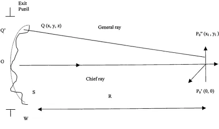
expressed as the derivative of wavefront error in terms ofpupil coordinates. In Figure
2.1.1, Po'Po" represents ray aberration, QQ' represents wave aberration. Figure 2.1.1 is
foron-axis case.
(xyi)=Rlni*(dWldx,dWldy) (2.1.1)
Where (x;, y;) are coordinates ofPo" with respect to Po', and R is the distance between
exit pupil plane and the image plane, n, is the refractive index on the image side, W
Exit
Punil
Q' Q (x,y, z) Generalray
0
Po"(xi,yi)
Po'
(0,0)
[image:16.540.52.496.62.323.2] [image:16.540.59.447.419.584.2]W
Figure 2.1.1 Aberratedwavefrontforan on-axis point object.
EntP
ExitP
AS
One mostly encounters rotationally symmetric optical systems like in Figure 2.1.2. The
wave aberration canbeexpressedas a power seriesintermsofobject/image(h) andpupil
(r)coordinates:
W(h{r) =
fjfjfjclpmh2l+mr2^cosm(6-eo)
(2.1.2)1=0p=0m=0
Where degree of each term ofthe series in object and pupil coordinates is always even
(2*(l+m+n)). We can removethe explicitdependence onimage heightby suppressingit
and also writingpupil coordinates as p=rl a
, where 'a'
is themaximum radius ofthe
exitplanepupil,9istheazimuthalangleinthepupilplane,we get:
W(p,e) =
fjfjanmp"cosme
(2.1.3)n=l m=0
Where anm = a"
JT
(2/+m)h'2l+m (2. 1.4) /=o
Theaboveis usuallywrittenas a sum ofmutuallyorthogonalpolynomials calledZernike
polynomials. Theseare givenby:
^(A^)=ZZc-[2("+1)/(l+3m0)]1/2C(P)cosAn6?
(2.1.5) n=0 m=0
Where cnmaretheexpansion coefficients whichdependontheimage heighth',and n and
(n-m)/2
K(p)=
Z
17 ^^F^r-^"2' (2-L6)Ho j!(n+m/2-j)!(n-m/2-j)!
istheradial polynomial ofdegreeninp.
The orthogonalityoftheradial polynomial andtheangularfunctionare givenby:
\k(p)K(p)pJp
=rrA,' (2-i-T)o 2(+l)
and
2/r
Jcosm,9cosm',^,9=;r(l+m0)Jmm, (2.1.8) o
Theexpansioncoefficientsare:
i in
cnm = (\//z)[2(n+\)(\+Sm0)T2\\W(p,S)R:(p)cosm3pdpd& (2.1.9) 0 0
Usingtheabove expressions one cancalculatethevariance oftheaberrationfunction:
*i=iicL (2.1.10)
11=1 m=0
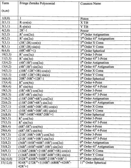
Anexample of someZernikepolynomials withthe aberration theyrepresentis shown in
Term
(n,m)
Fringe Zernike Polynomial Common Name
1(0,0) 1 Piston
2(1,1) R cos(ct) XTilt
3(1,1) R sin(a) YTilt
4(2,0) 2R2-1 Power
5(2,2) R2
cos(2a) 3rdOrder Astigmatism
6(2,2) R2
sin(2a) 3rdOrder45Astigmatism
7(3,1) (3R3-2R)cos(a)
3rd
Order X Coma
8(3,1) (3R3-2R)sin(a)
3rd
Order Y Coma
9(4,0) (6R4-6R2+1) 3rd
Order Spherical 10(3,3) R3 cos(3a) 3rd Order3-Point 11(3,3) R3 sin(3a) 3rd Order 45u3-Point
12(4,2) (4R4-3R2)cos(2a)
5th
Order Astigmatism
13(4,2) (4R4-3R2)sin(2a)
5th
Order45
Astigmatism
14(5,1) (10R5-12R3+3R)cos(a) 5th
Order X Coma
15(5,1) (10R5-12R3+3R)sin(a)
5th
Order Y Coma
16(6,0) 20R-30R4+12R2-1 5th
Order Spherical
17(4,4) R4cos(4a)
3rd Order 4-Point 18(4,4) R4 sin(4a) 3rd Order45u 4-Point
19(5,3) (5R5-4R3)cos(3a)
5th
Order 3-Point
20(5,3) (5R5-4R3)sin(3a)
5m
Order45u
3-Point
21(6,2) (15R6-20R4+6R2)cos(2a)
7th
Order Astigmatism
22(6,2) (15R6-20R4+6R2)sin(2a) 7thOrder45u
Astigmatism
23(7,1) (35R7-60R5+30R3-4R) cos(a)
7m
Order XComa
24(7,1) (35R7-60R5+30R3-4R)sin(a)
7th
Order YComa
25(8,0) 70RS-140R6+90R4-20R2+1 TOrderSpherical
26(5,5) R5 cos(5a) 3rd Order 5-Point 27(5,5) R5 sin(5a) 3rd Order45u 5-Point
28(6,4) (6R6-5R4)cos(4a)
5W
Order4-Point
29(6,4) (6R6-5R4)sin(4a)
5m
Order45u
4-Point
30(7,3) (21R7-30R5+10R3)cos(3a) TOrder3-Point
31(7,3) (21R7-30R5+10R3)sin(3a) TOrder
45u
3-Point
32(8,2) (56R8-105R6+60R4-10R2)cos(2a)
9th
OrderAstigmatism
33(8,2) (56R8-105R6+60R4-10R2)sin(2a)
9th
Order45u
Astigmatism
34(9,1) (126R9-280R7+210R5-60R3+5R) cos(a) } 9W
Order XComa
35(9,1) (1 26R9-280R7+2 10R5-60R3+5R)sin(a)
9th
Order YComa
36(10,0) 252R1U-630RS+560R6-210R4+30R2-1 9thOrderspherical
37(12,0) 924R,2-272Rlu+3 1 50RS-1
680R6+420R4-42R2+1
1lm
OrderSpherical
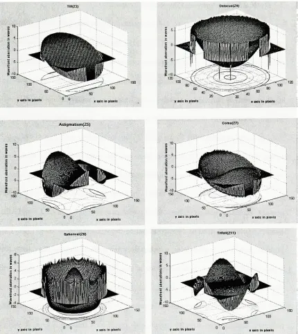
[image:19.540.50.493.85.654.2]Tllt(Z2)
yaxisIn pixels o a
Astigmatism(Z5)
id';;--0) i
5-c e
I 0- ;'-'\
:'3siBrlii Hii^laW. ^*.ffr^)%%Xfiat^HrMIIil^^B
^^^^~ -5,
fe
S mmHUHi^^^^
$ -10,
150
!Er7>^
'
^*-"V~-ISO too
^s^---." X'Y
'
^^^""^vn so
^>^ ^^50
yaxisInpixels 0 0 X axisInpixels
5-10
VaxisInpixels 0 ?
[image:20.541.58.488.83.566.2]yaxisInpixels
Figure 2.1.3: Sometypicalwavefrontplots
2.2 OpticalLithographyandProjectionSteppers
Lithography is the name for a sequence ofprocessing steps for structuring the
surface of planar substrates [9], [10], [11], [12].Wecandistinguish betweentwo types of
lithographicprocedures. Masklithographyandscanning lithography. Inmasklithography
thepatterntobetransferredisencoded as amplitudedistributionon amask, andthemask
is illuminated to transfer the pattern to the wafer. In scanning lithography a modulated
beam isusedto write patterns directlyonto thewafer. One can also distinguish between
variousforms oflithography bythe type ofilluminationtheyuse, such aselectronbeam,
x-ray, ion-beam, or optical. Electron beam and ion-beam are scanning type, x-ray and
optical are masktype.Electronbeamlithographyisusuallyusedformaskmaking.
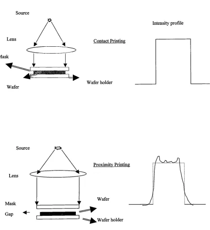
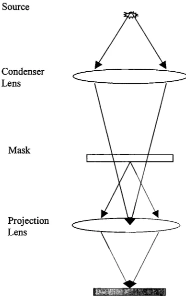
Optical lithography,whichistheworkhorse oftheindustry, canbeofthreetypes,
contact, proximity,and projection. Alloftheseareshowninfigure 2.2. Laand2.2. Lb. In
contactprintingthe maskis directlyplaced on thewafer and exposedto light. Themain
problem here is ofmask defects, which arise when mask is stripped repeatedly from the
wafer. Resolution down to two microns is possible. In proximity printing the mask is
placed a little away from the wafer. This reduces the wear and tear in the mask but
diffraction effects reduce resolution. Inprojectionprinting animageofthephotomaskis
projected directly onto a wafer coated with photoresist through a lens. A variation of
above isscanning orstep and repeat projectioninwhich a portion ofthemaskis imaged
onto the wafer andthe exposure repeated by either scanningor stepping over the entire
Source
Mask
Wafer
Intensityprofile
ContactPrinting
Waferholder
Source
Lens
Mask
Gap
Proximity Printing
Wafer
[image:22.540.61.493.105.577.2]Wafer holder
Source
Condenser
Lens
Mask
Projection
Lens
[image:23.540.131.317.95.393.2]Wafer
Thebasic components of a projection stepper are 1) illuminationsystem 2) lens 3)mask
holder4)waferholderand5)alignment system.
1) Illumination system: An example ofthe two extreme cases, coherent andincoherent
illumination is showninFigure 2.2.2. In newsteppers available now one can change
the coherence factor. UsuallyaKohlertype illuminationis used [30]. The technique
offocusingthe illumination source inthe entrancepupil ofthe imageforming optics
iscalledKohler illumination. Thisensuresuniformilluminationoverthefield.
2) Projection lenses: Thelensesused forprojection are some ofthebestmade andhave
near diffraction- limited performance. Projection lenses have become more
complicated withhigherdemands placedonthem. A listofsome ofthelensesbeing,
and to be used in IC manufacturing is shown in Table 2.2.1. The lenses are usually
telecentric. The exit pupil of atelecentric lithography lens is located at infinity, this
implies that each point onthe waferis illuminated with a cone oflightwhose axis is
perpendicularto thewafersurface.
3) Mask holder: It is basicallya stage forholding themask. Thestage canbemoved in
'x' and
*y'
directions, wherethe optic axis ofthe systemis along 'z' axis. Themask
MTF
1
Coherent
v/v0
Lightsource Condenser Mask Objective
Incoherent
[image:25.540.58.487.68.640.2]Partially coherent
Figure 2.2.2 Coherentandincoherentillumination,vis
the spatialfrequencyandvo isthecutoff spatial
Minimum feature
inmicrons
NA X(nm) ki Resolution
inmicrons
Depth ofFocus
(DOF)
in microns
1 .38 436 .8 .92 3.02
.7 .4 365 .75 .7 2.28
.5 .48 365 .6 .46 1.58
.35 .6 365 .5 .35 1.01
.25 .6 248 .6 .25 .69
[image:26.540.51.484.83.337.2].18 .6 193 .5 .17 .54
Table 2.2.1: Microlithographic lenses for ICproduction[1].
4) Waferholder: This isa stage toholdthewaferinplaceusingvacuum, whileit is
exposed.This stagehasthefreedomtobemovedalongallthe3 axes.
5) Alignmentsystem: Usuallyuses interferometrictechniques to align themask and
the wafer. Also helpsthewafer holdertobemoved accuratelywhile scanning or
2.3 Image Metrics
Theperformance of a stepperlens canbemeasuredorspecifiedinthefollowingways:
1) Resolution:
W=
^-
(2.3.1)NA
whereki isaconstant,whichdependson processparameters, X issource wavelength
andNAtheNumerical Apertureofthelens.
Thisequation explainsthe trendfor lowerwavelengthandhigher NAlenses. The
resolutionpossibleforvariouslenses is shownin Table 2.2.1
2) Depth ofFocus (DOF):
DOF=
Mr
(2.3.2)NA2
wherek2is aconstant,whichdependsonprocess parameters.Thedepthoffocus
values forvariouslenses isgivenin Table 2.2.1. DOFreduces whenonelowers
wavelength, orincreases NA.
3)Modulation transferfunction(MTF) [30]. Thisistheratioofcontrastin imageto
thatinobject,asfunction ofspatial frequency. Given by:
MTF(v)=
(2/x)[Cos-\v/v0)-v/v0(l-(v/v0)2f/2] (2.3.3)
Where vo=2NA/A. for incoherent illumination
andvo=NA/A,for
coherent
illumination.
Where
MTFP(cr,v)=
G(a,v)MTF(v) (2.3.4)
1
Gicr,v)=
4 forv<vx
1 sin( )
n 2NA ^ oW V2^ \(V~Vl) 1 sin(^ ) ' ' ' ' Si' i/l
-forvx < v< v.
n 2NA (v-v2)
(2.3.5)
1
sin(-;r
2JV4'
<\forv2 < v
wherev, = (1
-cr) andv, =(1+
.18cr) 1
A 2 X
aisthedegreeof coherence givenby:
CT=^
<2-3-6>WhereNAcisNumerical Apertureof condenserlens,NA0istheNumerical Aperture oftheobjective.
The MTF Plots forthe threekindsofilluminationis shownin Figure 2.2.2.
4) Strehlratio (SR): Thisistheratioofimageintensityaffectedbyaberrationsto
thatoftheimageintensitywithoutanyaberrations.
Acommon methodtoquantifytheamountofaberrationinalens istospecifythe
root-mean square(RMS) deviationofthewavefrontaberration. Forfringe Zernikesthisis
RMS'ik^^ikeJ (2.3.7)
m
Where sm =k/2(n+
1),nistheorder oftheradialpolynomial,k is 1 for
non-rotationally symmetric,and2 forrotationallysymmetricpolynomial.Onecan getthe
Strehlratio(SR)fromRMS using:
SR(R)= (2.3.8)
whereko=
2*n/X, Xiswavelength.
5) NILS (Normalized ImageLog Slope) [1]
1 r)F Givenby: NILS=L
(2.3.9) E0 dx
whereEois averageexposuredoseandListhelinewidth.
Fractionalchangein linewidthisrelatedtofractionalchangeinexposuredose by:
7=
2(M5)"^
(2.3.10)This impliesthatasNILSdecreases sodoesexposurelatitude. This doesnotuniquely
determineopticalcontributiontoprocesslatitude,because itdependson printbias
too.Anexample ofNILS isshownin Figure 2.3.1.
6) Process Window
This isa plot of usabledepthoffocusas afunctionof exposuredose.Thepresence of
aberrationsreducesthiswindow soitisausefulwaytodeterminethestepper
softwareforlithographymodeling) isshownin Figure2.3.2fora365 nmstepper
withlenshavinganNAof0.5 forcoherentillumination foraniso line500nm wide.
Intensity
248nm,NA=. 54
365 nm, NA=. 6
-300 -ioo 100
Distance fromcenter of space(nm)
Figure 2.3.1a: Lightintensity distributionof a350nmisolated(iso)space atbestfocus.
.05
248nm,NA=. 54
Normalized
Derivative
365nm,NA=. 6
-200 -100 0 100 200
Distancefromright edge of space
Figure2.3.1.b: Normalized derivative ofthelightintensity
distribution. Normalized derivative isinunits ofum [30].Asseen
[image:30.540.125.403.178.337.2]Process Window
Exposure Delta
(%)
100
CD
Sidewall Angle
ResistLoss
Overlap
-1.0 -0.5 0.0 0.5 1.0
[image:31.540.113.448.183.387.2]Focus
(um)
Figure 2.3.2: Process Window for 365nm,.5NAstepper withcoherent
illuminationfora500nmisolated(iso)line. Theseplotsindicateusable exposure
andfocus latitudew.r.tparameterslike CriticalDimension(CD), Sidewall
Angle(Profileofthe step),andResist Loss. Intheregionsinsidetheshowninside
thecontourstheparameters are within acceptablelimits. The overlapof allthese
showstheusableexposureandfocuslatitudewith which alltheseparameters are
2.4 Effectofaberrations onlithographic images.
Therelationbetweentheimage inthefilmatimageplane and wave aberrations canbe
written as[13]
I(x,y,z) =
\lda0d/30J(a0,/30)
\ E(x,y,z :a0,/30)\2
(2.4.1)
Where Etheelectricfieldattheimageplaneandcanbewrittenas
E(x,y,z:a0,/30) = FT'1
{b(a
-a0,P
-f30)P(a,[3)F(a,/3:z)eik^eik"W{a^
(2.4.2)
Where
FT"
is theinverse FourierTransform, J (ao,Po)is theeffective sourcedistribution
in the projection lens entrance pupil with area S. O (ot-ao,P-Po) is the shifted Fourier
transformoftheobject. P (a,P) istheprojectionlens transmission function. F (a,P: z) is
the thinfilm contribution withinthe photoresistto adepth of'z'. e^
is the focus phase
term. elkW(a'P)
is the contribution due to the wave aberration. Here ko =
2*ti/X, X is the
wavelengthofillumination. Using the aboveequation or slightlymodified versions ofit
the effect ofindividual aberrationshavebeen modeledby inputting individualaberration
terms in the wavefront term W(a,p) (The individual Zernike terms are shownin Table
2.2.2).
Looking at the aberrations term by term, the following generalizations can be
-The piston term Zi indicates constant phase over the aperture and does not affect
imagery.
Z2 andZ3representtiltoftheOptical Path Difference(OPD)wavefront, andtheeffect on
imagingisa positionalshift oftheimage inx ory directionontheimageplane.This shift
canberepresented as a vector proportional to theZernike coefficients. This can be seen
in Figure 2.4.1 wherethe aerial imageof a500 nmisolated (iso)line is shownfor a365
nm, 0.5 NAstepper,with no aberrations,andwith0.05wavesofxcomaaberration.
Z4 represents defocus. OPD surface is quadratic, and it degrades image contrast, edge
slope, pattern fidelity, and resolution. Z5 and Z6 represent astigmatism. OPD is saddle
shaped, and shifts orthogonal lines positively and negatively. For Z$ the shift is for horizontalandverticallines,forZ5theorthogonallines are noworiented at+-45 . Z7and
Zg represent coma andimage contribution from differentpupil radii shiftrelative to one
another. Z10 and Zn represent three clover. OPD has 3-fold symmetry and causes
undesirableimaging artifacts.Z9representsthirdorder spherical. OPDis 3rd
order surface
andthefocus shift acrosstheimagevarieswithp.Thiseffectis shownin Figure 2.4.1.
Theeffectof aberrationscanbe inferred in manyways.
1)Aerial Image: Aerial image isaffectedbyaberrations and canbesimulatedusingthe
equation2.4.1 shownearly inthesection. Figure 2.4.1 shows simulationdone using
Prolith fora500nmiso-lineon365 nm, 0.5 NAstepperilluminatedwith coherent
Aerial Image
(Relative Intensity)
-400 -200 0 200
X Position -(nm)
[image:34.541.83.475.96.362.2]400
Figure 2.4.1: Aerialimageof a500nmiso lineimagedbya365nm,0.5 NAstepper.
A-withoutaberrations, B- with0.05waves ofcomaaberration, C-with0.05 waveofspherical
aberration.These plots showtherelative intensityatdifferentfocuspositions. Aslice parallel
tox-axisatazposition willindicateintensityvariationalongxatthatzlocation.
Aerial Image
(Relative Intensity)
Aerial Image
(RelativeIntensity)
-400 -200 0 200 X Position (nm)
400 /: 1.29 1.17 1.06 0.94 0.82 0.70 0.59 0.47 0.35 0.24 0.12 0.00
Efled91.1vrev9corn, berrotai onktMgeo( ctoMed ipaee 1.5 Y r3ra A 1.2 X I 105 0S3 a3 0.15
an bJ I V-i.
~i
r-AberjoledSpacs M
' SpeoaM
I I I 0C 1.0 10 10 4.0 SO 60 7-0 8.0 10 TOO
X-flMS
MTF
Normalizedfrequency
B
Figure2.4.2: Thefirst figureAshowsPSFwithout,and with.1 waves of coma aberration.
ThesecondfigureBshows variationMTFwithvarious aberrations.
In B is fornoaberration, is forsphericalaberration^ is forcomaaberration,
[image:35.541.41.525.69.571.2]2)MTForPSF: Aberrations changethe MTF characteristic of alens. Onecan alsolook
at thechange in PSF. MTF and PSF are Fourier Transformpairs of each other [32]. An
example of non-aberratedPSF andMTF, alongwithPSF and MTF foran opticwith 0.1
waves of comaaberration are showninFigure 2.4.2. Whenaberrations arelessthanA/14
RMS, the shape ofthe central core of the PSF is essentially unchanged except for a
decreaseinpeakintensity.
3)Process Window: Theeffect of aberrations canalsobeseenas areductioninprocess
window.This is shownin Figure 2.4.3 whereProcess Windowfora365 nm,.5NA
stepperisshown with0.05 wavesofcoma,0.05 wavesofspherical,and no aberrations
forthecases of coherent andpartiallycoherentillumination (a=0.5).
Process Window
Exposure Delta(%)
100t
50
0
-50
-100
-1.0 -0.5 0.0 0.5 1.0
Focus(um)
y-~\
^CD
SidewallAngle
ResistLoss ~
Overlap
(A)Withno aberration.
Process Window
Exposure Delta (%)
100ir 50
0
-50
-100 -i i i
i--1.0 -0.5 0.0 0.5 1.0
Focus(um)
Process Window
Exposure Delta(%)
100
50
0
-50
-100
-1.0 -0.5 0.0 0.5 1.0
Focus(um) nuuess vviiiuuw . u^ ^^'***\ -J"4i^^_
1 1 1 1 1 1 1
CD Sidewall Angle Resist Loss Overlap CD Sidewall Angle Resist Loss Overlap
(B)With 0.05 waves of sphericalaberration. Coherent
illiimirmtinn
(C) With 0.05 wavesof
Coma.Coherent
Exposure Delta
-100
-1.0 -0.5 0.0 0.5 1.0
Focus(um)
CD
SidewallAngle
Resist Loss
Overlap (D)Withnoaberrations.
ProcessWindow
CD
Sidewall Angle
Resist Loss
Overlap
-1.0 -0.5 0.0 0.5
Focus(um)
1.0 (E)With 0.05waves of spherical aberration.Partiallycoherent
illumination
Process Window
Exposure Delta(%)
CD
SidewallAngle
Resist Loss
Overlap
-0.5 0.0 0.5
Focus(um)
0 (F)
With 0.05waves of coma
aberration. Partiallycoherent
[image:38.540.82.492.83.595.2]illumination.
Figure 2.4.3: Alltheabove shown simulations weredoneonProlith fora365nm,0.5NAstepperimaging
aniso line.A, B,Careforcohereiftillumination,D,E,Fareforpartiallycoherentilluminationfora=.5.As
3) Strehl'sRatio: Thefollowingresults shownin Figure2.4.4 arefromasimulation
doneatIBM [31],theoptical system consideredisa257nm, .35NA lenswith
partiallycoherentillumination (ct=0. 6). Ineachcasetheaberration valueis 0.02
waves. Thefollowingindicatecombinations chosen,a) Spherical+is
Zl1+Z22+Z37, b) Spherical-isZl
1-Z22+Z37,c) Coma+isZ7+Z16+Z29, d)
Coma- is
Z7-Z16+Z29,e)Astigmatism+isZ5+Z12+Z23,f)Astigmatism-is
Z5-Z12+Z23, g) Combination+is Z5+Z7+Z11+Z12+Z16+Z22+Z23+Z37, h)
Combination- is Z5+Z7-Z11-Z12-Z16+Z22+Z23+Z37.
Z'sindicate Zernike
coefficients(The individualZerniketermsare showninTable 2.2.2).
.9
.8
.7
Strehl's
ratio
-2 -1 0
[image:39.540.39.507.388.639.2]Defocus (um)
Figure 2.3:Strehl'sratiothroughfocus for
variousaberrations.
Noaberrations
a,b,c,d,e,f
3Experimental Procedures
Inthischapterthe experimentalprocedure usedisexplained.
3.1 Phase shiftingpointdiffractioninterferometry.
In point diffraction interferomtry [15] a beam diffracted from a pinhole in the
object plane falls on the test optic and the beam after passingthrough the optic passes
through a partially transmitting screen with a sub-resolution pinhole in it as shown in
Figure 3.1.1. The sub-resolution pinhole diffracts a reference beam and this interferes
with the transmitted beam to form an interference pattern. For accurate analysis ofthe
static fringe pattern, a significant number of tilt fringes need to be introduced by
displacement ofthe reference pinholelaterallyfromthe focusofthe testoptic. The light
intensity gettingto the sub-resolution pinhole is reduced. This with the small size ofthe
sub-resolution pinhole necessitates reduction of the intensity of the test wave by
attenuation.
This technique was modified by H Medeki, et al [16] with the possibility of
introducingphase shiftbyusing agrating. In this setup as shownin Figure 3.1.2 a small
pinhole atthe object plane ofthe optic to be testedproduces anearly spherical beamto
illuminate agrating kept in betweenthe optic and the object point. The gratingpitch and
thedistance between the grating andobject side pinhole are chosen so thatmore than 2
diffractionorders pass through theoptic. Intheimageplanetwo ofthediffractionorders
are spatially filtered with a mask which has one window, and a sub resolution pinhole,
The first order beamis made to pass throughthe largepinhole (approximately20 to 40
times the resolution limit ofthe optic) in a mask kept the image plane and is the test
beam. The sub resolution pinhole allows the zeroth order beam to pass through,
generating the reference beam. The reference and the test beam interfere to produce an
interferencepattern, which can be analyzed to get the wavefront phase error due to the
testoptic. The grating allows forthepossibilityofvaryingphase. Bymovingthegrating
in a directionperpendiculartoboth theoptic axis and thedirection ofgratingrulingsby
onefourthofthe gratingpitch, thephase ofthe 1storderbeamchangesby90 degrees and
that ofthezeroth orderisunaltered. Thiscan beusedto generate a set ofinterferograms
shiftedwith respectto each otherby90 degrees,which inturn canbe analyzedusing
5-framemethod [25](The method isexplained in section3.3). The accuracy ofthemethod
depends on various parameters, the most important being the quality ofthe reference
wavefront, which in turn is dependent onthe size ofthe sub-resolution pinhole. Other
factors are the 3rd order comaerror dueto the geometryofthe setup. This effect canbe
usedtocalibratethe interferometer.We can usea maskwithtwo sub-resolutionpinholes,
and compare the experimentallycalculated coma to the theoretically predicted value of
coma. Anotherpossible source of errorisdetectormisalignment.Alotof work onPSPDI
has been done bythegroup atthe department ofElectrical Engineeringat University of
CaliforniaBerkeley, wheretheyusedthemethod to characterizeEUVcameras [17], [18],
Optic
Source
CCD
Pinhole Mask
Transparentmask
[image:42.540.88.457.105.267.2]Withpinhole
Figure 3.1.1: Pointdiffractioninterferometrysetup.
CCDCamera
Pinholemask
Twopinholemask
[image:42.540.125.425.369.537.2]3.2 Errorsourcesintheexperimentalset-up
3.2.1 Errorduetoaparallel glass platebeingintroducedinaconvergingor
divergingbeamoflight (Figure3.2.1).
The gratingpattern andtheimageplane pinhole mask arebothwrittenon0.09 inches
thickchrome plated glass plates.Theparallel glass plateintroduces primary
aberrations whentheyareinthepath ofaconvergingordivergingbeamasisthecase
forthegratingand pinhole mask plate[8]. Theseaberrations canbeexpressedas:
W(r,0 :h)=
as(r4
-Ahr"
cos0+4h2r2
cos2 6+
2h2r2
-4h3rcos0) (3.2.1)
whereasis thecoefficientofspherical aberrationandisgivenby:
(n2-\)t as - r~r~
(3.2.2)
8n3S4
Letusmake anorder ofmagnitudecalculation oftheaberrationforthegratingplate.
Fromthefigure it isseenthat(r/S)~NA."n"
istherefractiveindexofglass,"S"isthe
separationbetweenglass plate andimageplane, "t"
isthethicknessofthe plate,"r"is
beam diameterattheplate. Thefirstterm ofequation3.2.1 willthenwillbe:
(n2-l)tNA4
1 (3.2.3)
8n3 V '
Usingthisandthe values, t=2286um,NA=0.028ontheobjectside,n=1.5 we getW
tobeoftheorderof6*
10"5
microns,whichisnegligible.
Ontheimagesidethepinholemaskis aligned suchthat thechrome coated part ofthe
patterngeneratedbetweenthereference andtestbeam. Wecanonlyreduceitby
usingtheminnest glass or quartz plate possible.
[image:44.540.67.453.130.325.2]ExitP
Figure 3.2.1: Parallelglassplate inaconverging beam. Raysincident
onplateconvergetoP' insteadofP.
.1
.05
P-V Phase Error
(waves)
-20
0
Linearphaseshift error(%)
20
Figure3.2.2: Measured Phase Errorvslinearphase shift error of
[image:44.540.55.449.377.626.2]3.2.2 Error incalculated wavefrontdueto errorin gratingmotion.
Asdescribedinsection3.1 on experimental procedurethegratingneedstobe
movedbya value equaltoonefourththatofthegratingpitch.Theerrorcanbereduced,
byusingalargegratingconstant so that therequiredmovementofgratingiscoarse
enough. Inthepresentset-up thegratingneedstobemovedby20microns,whichis
coarseenoughforthe stagesbeingused withleastcount of1 micron.Also as seenin
figure 3.2.2 [251,me use of5-bucketalgorithmimpliesthatthewavefront errordueto
errorin gratingmotionis approximatelylessthan0.002wavesforerrorsinmotion of
grating upto +-5%.
3.2.3 Referencepinhole errors
Asthepinholediameter isoffinitesize,itallowsfor finitespatial frequency
bandwidthtopassthrough. Itisreasonabletoassumethattheseerrorsdecorrelateas a
functionof pinhole positionrelativetothepoint spreadfunctionoftheoptic.Thiseffect
canbemitigated,byanaveragingprocess wherein pinholepositionis changedbya
fractionoftheopticpoint spreadfunction. Theothersource of erroris defectsinpinhole
shapethatistheholesbeingdifferentfromperfectcircles.Thiscanbereduced,by
averagingoveranensembleofequivalentsizedpinholes [24].
Forthisparticular experimentdoneontheopticbench, another source of erroris
micron,andthesize ofthepinhole usedinthemeasurementset-up isof2microns. A
micron pinhole waswritten,but didnot clearfullypossiblybecauseof wetetching done
on athickchromelayer. Modelingwasdonetoget anideaofwhaterrors anon-ideal
pinhole wouldintroduce.Theassumption wasthatidealpinhole was adeltafunction,and
thenon-idealwas a rectfunctiontwice thesize oftheideal. Theassumptionisvalid
becausetheFouriertransformof a 1 pixelimagegivestheresponseexpectedfrom ideal
deltafunction The farfield diffractionfield, whichrepresentsthewavefrontattheexit
pupil,was calculatedfortheidealand non-ideal reference pinholeand asetof37 Zernike
polynomialsfittedto theportion ofdifferencewavefrontfillinganNAof0.28. Thiswill
indicatethesystematic errorduetonon-ideal pinhole.A firstapproximationto thefar
fieldwavefrontdiffracted fromtheexperimental pinholeis thediffractionpattern ofa
coherentbeam fromasimple circular apertureinaplanar screenbasedonKirchofFs
modelofdiffraction theory.Apinhole ofdiameter, d, diffracts aspherical wavefrontthat
fillsNA= sinG= 1
.22A,/d.The Zernikecoefficients calculatedfornon-idealpinholefor
the436nmoptic are shownin Figure 3.2.3. Thenon-ideal 2-micronunderfillstheNAof
opticbyapproximately 5percent. Thecalculatederror wavefronthasnon-zero valuesfor
theaberrationtermsZ9andZ17. Thefirstoftheseis importantasthesecond one can
possibly bereducedorremovedbyPark'smethod [AppendixB],itbeingan
3.2.4: Systematicgeometric effectofcoma
Becauseoftheinherent largetiltintheset-up thereisasystematiccoma errorin
thereconstructed wavefront[19, 21,24]. Assumingtheseparationbetweenthereference
pinholeandthewindowtoliealongxaxis andexpressingrr,andX2(Figure3.2.4)asa
functionofmixingplane positioninpolarcoordinates(p,0)andbynotneglecting higher
ordertermswehave
g -0.05
-D.15
Error duetolargerreferencepinhole
-l 1
r-15 20 25
zemcoeffno
40
Figure3.2.3: Error duetolargerreferencepinhole.Theabove plot
showstheZernikecoefficients forthecalculateddifference
wavefront,betweentheidealsizedpinholeofdiameterdandthenon
[image:47.540.70.391.303.558.2]Ar=rx-r2=(-^3 --(f]p)Cos0 (3.2.4)
2z z 2z
where sisthe separationbetweenpinholes,zistheseparationbetweentheimageplane
andthepinhole plane.
IntermsofZernikepolynomialstheabove equation canbewritten as:
Ar=
(C(3p3-2p)+Tp)cos0 (3.2.5)
Where C isthecoma coefficient andTis tiltcoefficientalongxdirection.
C= =
(sin"1
(JM)) -(NA? (3.2.6)
6 z 6 6
Thiscanbeusedtocalibratetheset-up. Ifweusetwosub-resolutionpinholesinthe
imageplanemask, andthenmeasurethewavefrontit shouldyieldonlythe tiltand
systematic comaerror,becausenowtworeferencebeamsareinterfering.Comparingthe
calculatedsystematic comawiththeoretical one, theset-upcanbecalibrated. This
calibrationcould notbeen done for 436nmoptic asthe2referencepinhole mask was not
written.Thevaluesin bothcases wouldbe 1 micronfor 436nm,and.16micronsforthe
248 nm.
3.2.5: Detectormisalignmenteffect
Properalignment needsthedetectortobeperpendicularto thecentralrayofthe
tilt yx, andyywith respecttox and y-axesrespectivelyas showninfigure3.2.5,then the
pathlengtherrordueto thisisgiven as:
Ar =
^j[yx(cos20
+l)-yy
sin20]2z (3.2.7)
Thiscanbeinterpreted intermsof astigmatism anddefocuserrors andcorresponding
coefficients are givenrespectivelyas:
and
ea=\NA\yx2+y2r2
1
(3.2.8)
ed = (3.2.9)
whereNA=rm/z
Thevalues wouldbe 0.000154waves(ea), 0.000054waves(ed)for436nm perdegreeof
tilt.
2-pinhole
mask
I
Figure 3.2.4: Systematicgeometric effect of coma.Mixing
[image:49.540.82.354.462.620.2]3.2.6:Errorduetoscatteringofreferencebeamthroughthespatialwindow
Inthepresent experimenttheseparationbetweenthereference pinhole andthe
spatial windowisequalto thewidth ofthewindow[23]. Inthiscasethereis apossibility
of referencebeambeingscatteredthrough thewindow.
Signal reachingthedetector is:
U(fx)=
A8(fx
-fe)+rect(^)[n(fx)+S(fx)]
Yy
Detectorplaneideal
[image:50.540.57.445.332.636.2]alignment
Figure 3.2.5: Detectormisalignment
effect.
whereWisthewidth ofthe window,5representsthe pinhole,n representsthenoise
(scatteredsignalfrompinholethrough the window),andSrepresentsthesignalenergy
passingthrough thewindow. This isshowninFigure 3.2.6. Thiscanbeavoidedby
changingtheseparationto 1.5times thewidthofthewindowinwhichcasethereisno
scatteringas seenin figure3.2.6.
w
k M ?
1
w
< ?
[image:51.540.58.439.331.498.2]f.
Figure 3.2.6: Thetoptwo figuresshowthe spatial spectrum ofthefield intherecording
plane, thebottomtwo figuresshow spatial spectrum of recordedirradiance. Thefigures in
theleftareforthecaseofseparationbetweenthepinhole andwindow equaltoWtheright
3.3The 5-framemethod.
Thismethod canbeused foranyinterference set-up, whichhasthe possibilityof
shiftingthephase ofthe interferencepattern [23], [24], [25]. Thephase shifting itselfcan
be doneinvarious ways. Someofthemethods employed forphaseshiftingarea) moving
mirror, inwhich a reference mirrorismoved inadirectionperpendicularto theopticaxis
using a piezo. b) tilted glass plate c) moving diffraction grating, in which a grating is
moved in a direction perpendicular to the optic axis and the grating ruling d) Rotating
Analyzeror Waveplate. If is the wavefront phasedifference between the test andthe
referencewavethen theIntensityofinterferencepatternrecorded canbewritten as:
I= I0(l+
yCosW)) (3.3.1)
This technique uses
90
phase shifts to minimize phase calibration errors. This
algorithm reduces thepossibilityofthenumerator and denominatortending to zero, and
thereby reduce the uncertainty in the calculation. It uses five frames ofintensity with
relative phaseshifts of a. Ioisthezeroorderintensity,yisthecontrastfunction.
/, =Io(l+yCos(0-2a))
I2=Io(l+yCos(0-a))
I,=Io(\+yCos(0)) (3.3.2)
I4=I0(l+rCos(</>+a))
Theseequations canbecombinedtoyield:
*\im/yS\ivi/h
(3.3.3)
I2-I4 SinaSintfi
2/3
-15
-Ix (1- 2Cos2a)Cos<t>
when a=
n/2theequation simplifiesto:
=tan-'[ 2(/z h) ] (3.3.4)
2/3-/5-/,
V[2(/2-/4)]2+(2/3-/5-/1)2
Thephasethusinferred fromthe interferogramisusuallywrappedintherangeof
0 to 27i, due to the nature of arctangent calculation. To get the correct phase of the
wavefrontthephase needs to beunwrapped. Therearemanymethods ofunwrappingthe
phase. Thebasic assumption all ofthesemethodsmakeis thatit isnotpossibletohavea
3.4 Phase unwrapping:
Phaseof wavefront whendeterminedbyinterferometricmethodsiswrappedin
therange of0to2n, and needstobeunwrapped. See Figure 3.4.1 as anexample.
Thesimplest method ofunwrappinginvolvesa sequentialscanningthroughofdataline
byline as shownin Figure 3.4.2 [26].While scanningthelineadjustment(aphaseof n
added orsubtracted) ismadeto thepixel valueswiththeassumptionthatphasevaries
smoothlyandneighboringpixelscannothave ajumpof morethann.Attheendof each
linethephasedifference betweenthecurrent pixel andthepixelontheline beloware
compared, corrected andthelinescannedintheoppositedirection. Thisimpliesthatwe
aretreatingthe2dimensional dataas wrapped one-dimensionaldata. Thisdoesnot work
always.
271
0
Unwrappedphase
Wrapped Phase
^
/
?/
/
?
V
N
?Figure 3.4.1: Arepresentation of
Phasewrapping.
An improvedversionwas givenTakeda [27]. Hereeach rowisindependently
unwrapped.Therows nowhaveanundeterminedphase relationtoeach other. This is
Line
by
line sequentialunwrappingAfter Scan 1
After
Scan 2
[image:55.540.29.219.113.258.2]Takeda'smethod
Figure 3.4.2: Schematicofunwrapping
byline-by-linemethodandTakeda's
4Experimentalset-up
Aprototype experiment wasdoneon an opticbenchusinga436nmCarl Zeiss
optic.Theset-upused was similarto thatshowninfigure3.1.2. Thesource used was a
He-Cd laserlasingat442nm.Theobject side pinhole was 10microns.The gratingused
hadapitch of80microns and waskeptadistanceof
'z'
awayfromtheobjectpinhole,
towards theoptic.The gratingwasfabricatedoncommerciallyavailable, chromeplated
glassmasksusinge-beam patterning.Theimagesidemaskwas alsofabricatedusing
e-beampatterning. Initiallythemask wasmadeoncommerciallyavailable, chrome plated
masks,butthesedidnothaveenoughattenuation. Soglass plates were coated with2000
angstroms of chrome andthenused. Theimage sidemaskhada set of pinholewritten
withthesmallpinhole sizesranging from 1 to 5microns,for 2differentseparations,27.5
and50microns, correspondingto 'z'
valuesof50 and90mm.Thepinhole pair with
1-micronsize didnot clearinthe mask; possibly duetotheinabilityof wet etchtoclearthe
thickerchrome. Fromthedata intheTable 4. 1 thedistancebetweenthefrontlenssurface
andobjectplaneis 440.5 mm andthedistance between last lenssurface andimageplane
is 29.4mm.
For recordingtheinterferogramanLBA 100 laser beamanalyzerset-upwas used.
The LBA 100usesapulnix CCDcamera(120by 120pixels). Thedatawastransferred
fromtheLBA 100to aPC usinganRS232 interface. Theinterferogram fileswere
program writtenin-house forthepurpose[Sourcecodeis inAppendixC].Aset offive
typicalinterferograms isshownintheFigure5.1.
S-Planar 1.6750
Cat. No. 10 77 82
Reductionratio 1:10
Wavelengthrange 436+-5nm
Objectto Imagedistance 602+-4mm
Image fielddiameter 14.5mm
Square image format 10.5by 10.5mm
Flangefocaldistance 24.5
+-.3 mm
Free working distance Min 10mm
Lengthofbarrel 160.5 mm
Max. diameter 85.5mm
Screwthread M 76by 1
Entrancepupil
Locationbehindtheobject
Diameter
486mm
27.2mm
Exitpupil
Locationbehindtheimage
Diameter
512mm
287mm
Effective focal length 49.1mm
DistanceofPrincipalpoints +8 mm
Numerical aperture 0.28
Diffractionlimitofresolution 1285linepair per/mm
Rayleighdepth in imagespace +-2.8microns
Dataonimageperformance
1. Full field
Distortion max.+- 0.3microns
Opticaltransferfactor forincoherent/partiallycoherentillumination(o=0.5)
Spatialfrequency(lpper/mm) Linewidth(um) Optical Transferfunction(%)
250 2 59/92
500 1 37/62
2. Restrictedfield diameter 10mm
Distortion max. 0.2microns
Optical Transferfactor forincoherent/partiallycoherentillumination(a=0.5)
Spatial frequency(lpper/mm) Linewidth(um) Optical Transferfunction(%)
250 2 69/96
500 1 46/67
700 0.7 30/30
5 ResultsandAnalysis
The experiment was performed on a Carl Zeiss g line lens. The procedure is
explained in section 4.1. The experimental interferograms obtained for 0
orientation is
shown in figure 5.1. The Wavefront aberration of the lens was calculated using the
algorithms described. Park's method was used to remove theunsymmetrical aberrations
due to the reference beam. An averaging of 50 counts was done while taking each
interferogramtoremove or reducerandom errors. I used2fitting algorithms. These are
shownin appendixC. Each algorithm wasused to fitasyntheticwavefrontforwhichall
the Zernike coefficients were set to 0.1 waves. The difference or error wavefronts for
each algorithmwas calculated. The RMSforerrorwavefront afterfitting,usingalgorithm
1 was 0.00754waves, usingalgorithm2was 0.000247waves. Thevalueslooksmallbut
areimportantaswillbeseen.
A set of six interferograms eachhaving aphase difference of tc/2 w.r.ttheother
was taken forall the4 orientations. Wecan calculatethewavefront phaseusing 5-bucket
algorithm. Weshouldget comparable values when phaseis calculatedwiththefirst 5 or
thelast 5 interferogramsthatiseitherusingL, L, I3, L, andI5,orusingI2, 13, L, I5,andI6.
This should represent repeatability. The following plot Figure 5.2 shows the wavefront
coefficients calculatedusing algorithm 1 and 2 for90
orientation ofthe optic, byusing
Ilfff
Iff
\
j1 \w , il'j.]: ji! 'i:;';
'|j
:; ; ; 1
"' fi
;
j
| Ij
:;
fj
j.i 'j 'f !j'
j
i \ . Ml\\
'
\ i '
^ |
'
t , j ,Bj
';
|
i ii |m i' ', ;..' .
"
* '-: *' '
j'
I\ I : j
'
k1 \\\\\\ : :
i. j i ; '
|| j {
|
:-I 1;]^ II ij '
! ,,- !< !;
I'' i'
| ' j. jJ
'
* ;B'.| !'
!
I
!' '
'
' :
<
11
ft !l ii 1.. ! !, s, j j; ] i !-i jmIillii
1 ill 1 1
1
3 1 1
ll
ii
[
1 i M ft I Interferogram 1 Interferogram 3 !: I ' :|>1*
1f> '
t
'
f
!:J :| K | I i 1
|
;-'
j 1, ,
'
','
'
. I "'';
'
! !
1[%i
' i ; I I ' i --.. | h ; ' ;
\) i ! i
1
Interferogram 4
[image:60.540.28.493.81.714.2]Interferogram 2
Figure 5.1: Shows aset interferogramsshiftedw.r.t eachotherbyn/2. These interferogramswereimagedon a120by 120 Pulnix CCD
camera.
Interferogram 5
in ii
I !'! I
Repeatability </5 > CO CD o o N 0.35 0.3 0.25 0.2 0.15 0.1 0.05 0 -0.05 ' _J
fi
'[l
_JL n n12 3 4 5 6 17 8 9 11011 12 13||4 1516 1718(1 9 20 21 22 23 24 25 6 27 28/28 30 313233,3435 36 37
11st five
12ndfive
zern coeffno
Repeatability 0.06 CD > 0.04 CO C "2 g " d) N
XX flJH,
Ix.
1 2 3 4 51 6 7 8 9 10 1112 13 14 1516 17 181
i4ji
P'2?l
232425 26 27 28 29 BO B1LoJil
32IT:033435 36 37I
Q1stfive2nd five
zern coeff no B
Figure5.2: AshowsthewavefrontZernike coefficients calculated
usingalgorithm1. B shows wavefrontZernikecoefficients
calculatedusingalgorithm2.Foralgorithm 1 theRMS oferror
[image:61.540.61.482.113.542.2]Theabove plotsindicatethatrepeatability isgood andisindependentof algorithm.The
RMSvaluesforthewavefrontsmatchtowithin0.0056wavesforalgorithm1 andwithin
0.0009wavesforalgorithm2.Algorithm 1 hasmore errorintheestimatingthefollowing
coefficients9,10,15,16,17,28,36,37andthisiswhatleadsto thelargervaluesforthese
coefficientsinthecalculated wavefront.Thecomparison ofthe twoalgorithmsisshown
in Figure 5.3.
Tilt:The experimentallyobservedtiltintheinterferogram, inlinepairsper mm
(lp/mm)is: observedtiltis 9.8666waves or 19.73 lp/mmover8.5mmofCCD,thatis
2.32 lp/mm. Thecalculatedvaluefrom geometry usingyoung's doubleslit equation:tilt
in lp/mm isgivenbysl(X*Z). Where's' isthedistance betweenthepinholeandwindow
(27.5microns),
'A,'
isthewavelength(442nm), and 'Z'
is thedistancebetweenthe
pinhole maskandCCDplane(2.75cm). Puttinginthe values, the tiltis foundtobe 2.26
lp/mm.
Thevalues gotfrom usingalgorithm2were usedto calculatethewavefront
coefficients foreachofthe4orientationoftheoptic. Park'smethod(AppendixB)was
usedtocalculatethewavefront with reference errorsremoved.Figure 5.4showsthe
aberration coefficients ofthewavefrontafterapplying Park'smethod. Strehl'sRatio
Algorithmcomparision
0.102
> TO
5
03 >
8=
d) o o
o>
N 0.096
Dnewalg
oldalg
12 3 4 5 6 7 8 9 10 1112 13 14 15 16 17 18 19 20 2122232425 26 27 28 29 30 3132 33 34 35 36 37
[image:63.540.74.466.124.358.2]Zerncoefficient no
Figure 5.3: This showsthecomparison oftwoalgorithms usedtofit
thewavefrontandestimateZernikecoefficients.Herefitis donetoa
syntheticwavefront with each coefficienthavinga value of0.1. The
WavefrontcoeffafterPark'smetod
0.07 0.06 0.05 004
a>
ii 0.03
CO >
8 01
E o
CD N
-0.01
-0.02
-0.03
-0.04
12 3 4 5 6 7 S 9 10 11 12 13 14. 15 16 17 18 19 20 21,22 23 24 25 26 27 28,29 30 31 32 33 34 35 36 37
niJ
TV -crrrcr n
~
-n , _ n
\
1
'irir '
lii~'
11 '
f,r
ij-j
[image:64.540.60.476.125.298.2]zern coeff no
Figure 5.4: ThisshowstheZernike coefficients after
MTF
The MTF of an optical system withknownaberrations canbecalculatedusingan
equationfrom chapter4of'TheArt andScienceofOpticalDesign',byR.R. Shannon
[32].
Theequations are:
DTF(Q)= [arccos(fi)
-QVl-^2]
whereQ. =
71
V
V (5-1)
ATF(Cl) = 1
-(
^=-
J
(l
- 4(Q-0.5)2
)
MTF(0)=DTF(Ci)ATF(Q)
Intheabove equationsDTFistheaberrationfree MTFoflens,ATFistheaberration
transferlensdependingontheWavefront aberrationsofthelens(Wrms)- Figure5.5
showsthe calculatedMTF usingthecalculatedWrmsvalueof.0505waves,andtheMTF
MTF
-calculated -fromdatasheet
0.4 0.6 0.8
normalized spatialfreq
Figure 5.5: TheaboveshowsMTFplotsof436-nm
opticfromthedatasheet andfromcalculationusing
Total errorinthemeasurement:
1) Errorduetogratingglass plate: RMSof errorwavefrontis7.92*1
0"5
waves
2) Errorduetomeasurement(couldincludeerrorduetogratingmotion,but I have
consideredthatseparately):RMS of error wavefrontis 0.0009waves.
3) Errorduetomotion ofgrating assuming Imoveto within 1 micron: RMSof error
wavefrontis 0.001587waves.
4) Errorduetodetectortilt(assumingdetectortiltiswithin2degreestoaplane
normaltooptic axis): RMS of error wavefrontis 0.000188waves
Assumingtheseerrorstobe independentthe totalerrorcalculatedforthemeasured
6 Conclusions andRecommendations
The results obtained for the Zeiss lens show that PSPDI can be used for testingof
stepperlenses. The measured values of aberrations andStrehl's ratio are in the expected
order of magnitude. The analysis end has been verified and works fine. The things
learned are that one ofthe most crucial components is the sub-resolution pinhole. The
smallerthepinholeis, thebetterthe accuracyofthemeasured aberrations. Butonehasto keep also in mind that the smaller pinhole willreduce the contrast inthe interferogram.
The set-up canbecalibratedbyusinga2-sub-resolutionpinholemask andcalculatingthe
coma got from interferogram analysis, and comparingthe resultwith expected coma for
theset-up (refersection3.2.4). The gratingmotion needstobecalibrated and micrometer
stages with accuracy of 0.1 micron need to be used as mentioned in section 3.2.2. As
mentioned in section 3.2.3 for future measurements one needs to take averages of
measurementsbymovingthepinhole maskbyafractionoftheopticPSF and alsotaking
averages over a number of pinhole pairs. One can get abetterestimate ofthe total error
by doingthefollowing:
a) Measurementerror: Take 10interferogramsshifted w.r.t each otherbya phase of
ti/2, thisallowsforcalculation ofwavefrontphase 5times.This impliesI can
generate 10differencewavefronts. LetthestandarddeviationoftheRMS ofthese
b) Makeanother set ofmeasurementswiththeposition ofmicrometerscrewmoving
thegrating,movedby.2micronfrom idealpositionforeachofthefive
successive positions. Calculatethewavefront phaseforeachcase; calculatethe
differencewavefront w.r.tidealcase.Leta2bethestandarddeviationoftheRMS
ofthesedifferencewavefronts.
c) Let0-3 representtheRMSoftheerrorwavefrontduetoglassplate(grating)
d) Let cj4representtheRMSoftheerror wavefrontduetodetectortilt(assuming
detectorplaneisnormaltooptic axis within 1 degree).
Thetotal errorintheRMS ofmeasuredwavefrontthenis:
ct=(^+
^
+ct32+ct42)-5 (6.1)
10 5
Appendix A
Zernikefitting
WenowdiscussthevectorformulationforZernikepolynomial surface fittingand
extraction ofZernikecoefficients.Awavefront canberepresented as alinear
combination ofZernikepolynomials.
W(x,y)=
YJctjZj(x,y)
(1)In discreteform:
Wr(xr,yr)=
YjajZj(xr,yr)
(2)Where Wr (xr, yr) is the value of wavefront at point (xr, yr) and Zj's are Zernike
polynomials and a,-'s are the coefficients. Let there be n points (n>m). Usually m = 37.
Writingtheaboveinmatrixform
^iCWi)
W2(x2,y2)
^,(W).
^iCwi). -^(xp^i)
zx(x2,y2), zm(x2,>>2)
Writing
Wx
W.
using(3),equation(2) canbewritten as:
W=[ZbZg
ZyCWl)
~ax
zM2,y2)
=h> a2
zMn>y)_
-an_=a
-. Zm]*a
(4)
(5)
Letthemeasuredvalue of actual wavefront W begivenby Wl.Thensumof squaresis
givenby:
S= [Wl-[Z,,
-,Zm]*a]
thatis:
n m
r=\ j=\
S=
Y,(mr-ZajZAXr>yr)r
n
Now minimizing Sw.r.t
a,-weget:
(6)
(7)
YwKzA*r,yr)
=YLajzMr,yr)zk{xr,yr)
r=\ j=\
r=\
(8)
WIZ,
w\z
ZXZX,
~lZlZm
ZmZ\1 'ZmZn
(9)
ChoosingZ/stobeorthonormalonehas:
WIZ,
W1Z
ZxZx,0,-
0,Z2Z2,-
0,0,-o
,0
7 7
(10)
Thecoefficients canthenbewritten as:
Becausewe
![Table 1 : Technology roadmap for lithography [1].](https://thumb-us.123doks.com/thumbv2/123dok_us/121228.11692/13.540.50.455.249.432/table-technology-roadmap-for-lithography.webp)
![Figure 2.2.2thefrequency Coherent and incoherent illumination, v is spatial frequency and vo is the cutoff spatial [9].](https://thumb-us.123doks.com/thumbv2/123dok_us/121228.11692/25.540.58.487.68.640/figure-thefrequency-coherent-incoherent-illumination-spatial-frequency-spatial.webp)
![Table 2.2.1: Microlithographic lenses for IC production [1].](https://thumb-us.123doks.com/thumbv2/123dok_us/121228.11692/26.540.51.484.83.337/table-microlithographic-lenses-for-ic-production.webp)
![Figure increase and linewidththeexposure wavelength.latitudedistribution. This translates to byabove 2.3.1.b: Normalized derivative of light intensity Normalized derivative is in units of um [30]](https://thumb-us.123doks.com/thumbv2/123dok_us/121228.11692/30.540.125.403.178.337/linewidththeexposure-wavelength-latitudedistribution-translates-normalized-derivative-normalized-derivative.webp)