
Rochester Institute of Technology
RIT Scholar Works
Theses
Thesis/Dissertation Collections
10-1-2003
0.18 µm CMOS low power standard cell library
Suryadi Gunawan
Follow this and additional works at:
http://scholarworks.rit.edu/theses
This Thesis is brought to you for free and open access by the Thesis/Dissertation Collections at RIT Scholar Works. It has been accepted for inclusion
in Theses by an authorized administrator of RIT Scholar Works. For more information, please contact
Recommended Citation
0.18
~m
CMOS Low Power Standard Cell Library
by
Suryadi Gunawan
A Thesis Submitted
III
Partial Fulfillment of the Requirements for the Degree of
Master of Science
III
Computer Engineering
Dr. Kenneth
w.
Hsu
Professor, Department of Computer Engineering
Principal Advisor
Dr. Pratapa V. Reddy
Professor, Department of Computer Engineering
Committee Member
Dr. Karl Hirschman
Associate Professor, Department of Microelectronic Engineering
Committee Member
Department of Computer Engineering
Kate Gleason College of Engineering
Rochester Institute of Technology
Rochester, New York
Release Permission
Rochester Institute of Technology
0.18 Jlm CMOS Low Power Standard Cell Library
I, Suryadi Gunawan, hereby grant permission to Wallace Library of Rochester Institute of
Technology to reproduce my thesis in whole or in part. Any reproduction will not be
commercial use or profit.
Abstract
With
theincreasing
number oftransistorsin
a singleintegrated
circuit, poweris
becoming
one ofthemajorissues in integrated
circuitdevelopment.
This
issue
requiresadditionaleffort
from designers
in
ordertoproducelower
powerdesigns. The
purpose ofthis thesis
is
todevelop
a standard celllibrary
using
Taiwan
Semiconductor
Manufacturing
Company's 0.18-micron
CMOS
technology.The
library
cells consumeless
power compared to thevendorlibrary
providedby
MOSIS.
Although
a reductionin
power consumption
is
themainobjectivein
thiscelllibrary,
thetiming
delay
and area aretwo aspects thatcannot
be ignored.
However,
a sacrificehas
tobe
madein
timing
delay
or area
in
ordertoachievethegoal oflower
power.In
order to produce alibrary
that containslow
power cells, a newdesign
techniquemust
be
used whilekeeping
in
mind thatpower reduction should notadversely
affect othera spects o
ft
he
c ell.D
rawbacksi
np reviously p
ublishedd
esigntechniqueswill
be
analyzed and a newdesign
technique composed of parts of previous techniqueswill then
be
postulated.The
new technique will thenbe
compared against thebest
technique
currently
available.A
design
techniquefor
standard celllibrary
development
can
be
determined
based
ontheresults ofthatcomparison.The
newdesign
technique can thenbe
implemented
into
a celllibrary.
The
cellcell
library
will thenbe
compared to a similar technique usedby
the vendorlibrary,
determining
that the produced cells consumelower
amounts of power.Each
c ell willthen
be
characterizedby
timing
delay,
area, truthtables,
dimensions,
andinput
Acknowledgement
This
thesis could notbe
completed without thehelps
and supportsfrom
individuals
and companies.Therefore,
to recognize their efforts,I
wouldlike
to expressmy
gratitudeandthanks to:1.
Dr.
Kenneth W.
Hsu,
my
advisor,for
his
guidance, advice andhelp
from
choosing
the topicuntilthefinish
ofthe thesis.2.
Dr.
Pratapa V.
Reddy
andDr. Karl
Hirschman,
my
thesiscommitteemembers,for
thesissuggestions.3.
My
family
for
theirfinancial
support and encouragement.4.
Tanner
Research,
Inc for
the permission to use theirDigital Low Power
Standard Cell
Library
for MOSIS TSMC CMOS 0.25
umProcess
Deep
Sub-Micron Technology.
5.
Mentor
Graphic
for
theirsupportto solve simulationtoolproblems.6.
MOSIS
for
theirTSMC
CMOS 0. 1 8
urn process parametersAlso,
I
wouldlike
tosay
thanks to companies orindividuals
whoindirectly
helped
Table
of
Content 17
Abstract
iii
Acknowledgement
vList
ofFigures
ix
1. Introduction
1
2. MOSFET
Modeling
6
2.1. MOS Structure
with4
Terminals
6
2. 1
.1
.Drain
Current Behavior
7
2.1.2. Gate
capacitancebehavior
14
2.1.3.
Small
Geometry
Effects
15
2.2. BSIM3
22
3. Power Dissipation in CMOS Circuit
25
3.1. Types
ofPower Dissipation
25
3.2. StaticPower
25
3.3. Dynamic Power
29
3.4.
Short Circuit Power
30
3.5. Total Power Dissipated
32
4. Low Power Design
Methodology
33
4.1.
Types
ofLow Power
33
4.2. LowVoltage
34
4.3. Low Average Power Consumption
35
4.4. Low Power Techniques
36
4.4. 1
.Changing
thelogic
style36
4.4.2. Logic
Restructuring
41
4.4.3.
Input
Ordering
44
4.4.4. Better Layout
46
4.4.5. Transistor
Sizing
49
4.4.6. Buffer
/
Keeper Usage
47
4.4.7. Gated Clock
51
4.4.8. Dual Voltage
51
5.2.2. I/O lines /port
56
5.2.3.
Geometry
56
5.2.4.
Routing
Metal
56
5.2.5. Placement
56
5.3. Published Standard Cell
Methodology
57
5.3.1. Example
Methodology
1
57
5.3.2. Example
Methodology
2
59
5.3.3. Example
Methodology
3
60
6. Development
Strategy
for Low Power CMOS Cells
62
6.1.
SPICE FILE
62
6.2. Power Reduction
63
6.2. 1
.Power
Supply
Reduction
63
6.2.2. Logic
Style
64
6.3. Experiment
71
7. Proposed Standard Cell
Library
80
7.1.
Standard Cell
Library Methodology
andDesign
Strategy
Implemented
80
7.2.
Standard Cell
Library
83
7.2.1. 1-BitAdder
84
7.2.2. 2x2 Input AND
OR Gate
(A022)
86
7.2.3. 2x2 Input AND NOR
Gate
(A0I22)
88
7.2.4. Non
Inverting
Buffer
(BUF1)
90
7.2.5. 4X Drive Buffer
(BUF4)
92
7.2.6. 4X Drive
Inverter
(BUFI4)
94
7.2.7. Tri
State Buffer
(BUFZ)
96
7.2.8. D
Flip Flop (DFF)
98
7.2.9. D
Flip Flop
withAsynchronous Clear
(DFFC)
100
7.2.10. D
Flip Flop
withAsynchronous Preset
(DFFP)
102
7.2.11. D
Flip Flop
withAsynchronous Preset
andClear
(DFFPC)
1 04
7.2.12. Inverter
(INV)
106
7.2.13. Dual Inverter
(INV2)
108
7.2.14. Tri
State Inverter
(INVZ)
110
7.2.15.
Latch(LAT)
112
7.2.16. Latch
withAsynchronous Clear
(LATC)
114
7.2. 17. Latch
withAsynchronous Preset
(LATP)
116
7.2.18. Latch
withAsynchronous Preset
andClear
(LATPC)
118
7.2.19. 2 Input Multiplexer
(MUX2)
120
7.2.20. 2 Input NAND
(NAND2)
122
7.2.21.
2 Input AND
(ATND2)
124
7.2.22. 3 Input NAND
(NAND3)
126
7.2.23. 3 Input AND
(AND3)
128
7.2.24. 4 Input NAND
(NAND4)
130
7.2.25. 4 Input
AND
(AND4)
132
7.2.27.
2 Input
OR
(0R2)
136
7.2.28.
3 Input NOR
(NOR3)
138
7.2.29. 3 Input OR
(OR3)
140
7.2.30.
4InputNOR(NOR4)
142
7.2.31.
4 Input OR
(OR4)
144
7.2.32. Schmitt Trigger Inverter
(SINV)
146
7.2.33. 2 Input Exclusive NOR
(XNOR2)
148
7.2.34.
2 Input Exclusive OR
(XOR2)
150
8. Conclusion
152
8.1.
Summary
152
8.2. Future Works
152
References
1 54
Appendix A
158
List
of
Figures
Figures
Figure 1-1. Heat
generatedby
CPU
4
Figure 2-1.4
terminalMOS
structure7
Figure 2-2.
Relationship
between
thedrain
current anddrain bias
11
Figure 2-3. The
gate capacitance oftheFET
structure14
Figure 2-4. FET depletion
regions showsthat the gateinduced
depletion
region overlapswiththesource and
drain depletion
regions16
Figure 2-5. FET depletion
region shows chargesharing between
thesource anddrain. 17
Figure 2-6. The
channel electronmobility
versus gate voltage of athinoxideFET
1 8
Figure
2-7. (a),
originalbarrier
withoutdrain bias
applied(b). Lowered barrier
afterthedrain bias
applied.The
dashed line
showstheexpectedbarrier
19
Figure 2-8. Potential
profilesin
FETs
with channeldopant
redistributiondue
tooxidation-enhanced
diffusion
21
Figure2-9.
BSHVI3
parameters23
Figure 3-1
.CMOS
modeldescribing
parasiticdiodes
26
Figure 3-2. Temperature
versusleakage
currentin different feature
size27
Figure 3-3.
Relation
subthreshold currentwiththeVgs in different Vt
28
Figure 3-4. Relation between Vt
and powersupply
depending
onthefeature
size .28
Figure 3-5. Circuit
modelload
29
Figure 3-6. Transient
waveform ofinverter
31
Figure
4-1. Standard CMOS
Architecture
37
Figure4-3.
Domino Logic Architecture
39
Figure 4-4.
Example
ofMCM Architecture
40
Figure4-5.
Power Dissipation
versusSupply
voltage41
Figure4-6. Adder
delay
versusSupply
voltage42
Figure 4-7. Transistor level
of8
inputs
NAND
gate42
Figure4-8. Schematic
of8 inputs NAND
gate40
Figure 4-9. Different implementation
of4
input AND
gate44
Figure 4-10. Two
input
NAND
power ratio45
Figure 4-11. Input ordering
effect on speed46
Figure 4-12. Elmore
delay
model47
Figure 4-13.
Two
different layout
techniquesin
creating
transistorwith wide width47
Figure 4-14. Power
consumptionis
not always minimized with minimumdevice sizing
50
Figure5-1. Example
offloorplan
55
Figure 5-2a.
Methodology
1
58
Figure 5-2b. Design strategy 1
58
Figure 5-3a.
Methodology
2
59
Figure 5-3b.
Design strategy 2
60
Figure 5-4a.
Methodology
3
61
Figure 5-4b. Design strategy 3
61
Figure 6-4. Selector
Logic
67
Figure
6-5.
Transmission
gatelogic
68
Figure6-6.
4
input
NAND using TGMOS logic
69
Figure 6-7. TGMOS logic
architecture70
Figure
6-8. Han Carlson Adder
72
Figure
6-9. Kogge Stone
adder72
Figure 6-10. Brent
Kung
adder73
Figure 6-11. 8-bit Han Carlson
adder74
Figure
6-12. 8-bit Han Carlson
adderlayout using TGMOS
library
75
Figure
6-13. 8-bit Han Carlson
adderlayout using
standardCMOS
library
75
Figure 6-14. 8-Bit Han
Carlson Adder Power Dissipation using
TGMOS
Cell
Library
76
Figure
6-15. 8-Bit Han Carlson Adder Power Dissipation using
Standard CMOS
Cell
76
Figure
6-16. 2
input
nandgateimplemented using TGMOS logic
78
Figure
6-17. 4
input
or gateimplemented using TGMOS logic
78
Figure 7-1.
Standard Cell
Methodology
used82
Figure 7-2. Cell
Strategy
used83
Tables
Table 1-1.
Battery
Comparison Worksheet
3
Table 1-2.
Battery
technology
comparison chart3
Table 4-1. Results
from
implemented
approaches of8-input
AND
gatein
lUm
CMOS
process
43
Table 6-2.
Power Dissipation
of2
input
norgate and4
input
nandgateimplemented
Chapter 1
Introduction
In
therecentyears, thedevelopment
ofVery
Large
Scale Integrated
Circuit
(VLSI)
has
advanced and crossed newboundaries
from
home computing
tomilitary
equipment.This
advancement
m akesi
tp
ossibletop
reduce powerfulp
ortable electronics, s uch a snotebook or
laptop
computers, personaldigital
assistants(PDA),
cell phones, tabletPCs
and so on.
These
systemshave
multiplefunctions
andincreased
capabilities over theirpredecessors.
For
example, cell phones can nowhave integrated PDA
capabilities suchas music playback,
built-in
cameras,creating
officedocuments,
and evenconnecting
tothe
internet. Notebook
computers are alsoincreasing
in
capability
andmay
soon replacedesktop
p
ersonal computers, especially
since
they
canp
erform advanced d igital
signal
processing
just
aswell ashome
computers.Multi-functionality
refersto theability
of adevice
tohave
thenecessary hardware
to accommodate multiple
functions.
For
example, a cell phone thatis integrated
with aPDA
musthave
anRF
transmitter to connect to the cellularnetwork, anLCD
screenfor
users to
interact
with,speakers tolisten
to music, and away for
userstobackup
data,
etc.This supporting hardware
requires additional power.In
addition, thedevice
mustbe
capable ofproducingresultsin
realtime.A
goodthe user's ear.
It
willbe
obsoleteif
the resultis
produced after a couple of minutes orhours
[4].
It
is known
thatmoreenergy
is
neededin
ordertoproducefast devices.
Yet
the examples of portable electronics mentioned above are able to executetheir
functions
with a portableenergy
sourceorabattery. Batteries
have
become
thelife
source
for
these portable electronics,meaning
theenergy
consumedfrom
thebattery
must
be
aslittle
as possiblein
ordertocontinue uninterrupted operation ofthedevices.
The
questionis
how
can we achievebetter efficiency
withhigher
speed andlower
power consumption?
Will
the solutionbe
abigger
orbetter
power source, so that eithertheuser
has
tobring
abigger device
orpay
moremoney
in
orderfor
thedevice
tooperateas
designed? How do
weinterpret
themeaning
of portability?Being
portableinvolves
greater
accessibility
andbeing
easy
to carry.A bigger
and more powerfulbattery
wouldmaketheportable
device
muchheavier
and sizewouldthenbe
anissue.
Will selling
thedevice
at ahigher
pricein
order to use abetter,
smallerbattery
be
a good solution?It
may be
feasible,
but
manufacturers want their products to sell quickly.Therefore
they
will
have
tokeep
theirpriceslow
enough to attract additional customers.The
tradeoffscan
be
seenin
table1-1
and table1-2.
NiMH,
NiCd
andLilon
are the threebattery
technologies that are
commonly
usedfor
portable electronics.Table 1-1
explains therelationship between
price,capacity
and size of thedifferent
battery
technologies.Furthermore,
abetter-performing battery
may
notnecessarily
mean a safer onefor
NiMH AA NiMH AA NiMH C NiCd AA NiCd AA NiCd C Lead Acid n/a
Cell Size Voltage
Capacity
(Ah)
Energy
(kJ)
Volume(cmA3) Weight(g)
1.2 1.2 1.2 1.2 1.2 1.2 12 1.3 5.62 1.9 8.21 4.0 17.2B O.B 2.59 1.D 4.32 2.5 10.B0 4.0 172.B0nA3| Wfeight
(g)
Cost kJ/$kJ/fl
kJ'CinA3 7.9 27 $0.66 B.51 0.21 0.717.9 27 $1.15 7.14 0.30 1.04 24.4 BD $2.33 7.42 0.22 0.71
7.9 21 $0.27 9.B0 0.12 0.33
7.9 21 $0.49 B.B2 0.21 0.55
24.4 72 $1.05 10.29 0.15 0.44
643 1B72 $8.40 20.57 0.10 0.27
Table1-1.
Battery
ComparisonWorksheet
[47]
I
' iManufacturer TypejChemistiy
LT ,INominal NominalL. , ,
Nominal' |_ iUsable
Voltage^
^f^^iCycles
iAmp-hrsWatt-hrs ;Watt
hr/kg
-Watt-hrf&er[discharge
[
rate
j
BYT 'AA [Lilon 3 6 ;0.75[2.7
600+ 135 365 1.5A1
! 'Tadiran AA [LiMetal 3 0 T8 [2.4 700 141 324 10mA
1
:|
1
~j
?told
Peak LAAJNiCad
jl.2
fl
1.2 46 :200J
Panasonic :AA |NiCad jl 2jl
[1.2 46 200Ijis
;AA|NiCad
jl.2
1|l-2
46 2001
TopPower:AA [NiCad
12 10.7 10.84 1000+ 3247
~
140
fBYD |AA
[MCad
|1.2[09
il.08 ;800+ 142 [18. 0A PowerStreatnAA(NiCad
12 jl 0jl.2
46 ;200[
;
i
!
Sanyo AA
(NiMH
112 1.5 [1.8i
69 246 Varta AA iNiMH 12jl.3
1.56 1000+j
70 213 3 9ATanasonic
^AA
NiMH !1 2jl.5
1.8 69 246BYD :AA [NiMH [1.2 1.3 ;15 '800+
;67 205 26.0A
I
'
GoldPeak [AA [NiMH
jl.2
16 1.9 600+[
72 259(js
AA NiMHjl
2|l
5 1.8 1I
69 246Harding ;AA
[NiMH
[12 1.5 18 '69 '246 KPowerStreaniAA
INMH
jl.2
J2.0
:2.4|
78 328; 1 1
1
Rayovac L, Rechargeable Alkaline
14to
09 1.6 :224
100+ 30 220
1
600mA
:
|
|
\[Evercel Box iNiZn 1.65
J24
139.6 500+(2) 49 [71 72.0A Evercel Box 'NiZn ;165 39[64
4 500+(2) 59 91 115 0AEvercel Box j'NiZn 12 22 264 500+(2) [12 74 72A
~|
||
|
!\B8cB
Box (SLA [12|12
1144 350+(l) ;36 103 PanasonicJBox
SLA [12 (12 il44 !37 991
fPowercache ,BoxjSupercapacitor;2.3 |100F ;0.15 200.000+ |4.1 15A
IPowercache Box JSupercapacitor
(2,3
.2500F 3.7 200,000+: 6 1800 AAnother
solutionis
to produce aless
powerful,slightly
slower and more power efficientdevice.
This
approach seems more reasonable,especially
withCMOS
(Complementary
Metal
Oxide
Semiconductor) being
thecurrently
usedtechnology..
CMOS
technology
has
been
proven tobe
alow-power
design,
andit
has been
shrunk tovery
small sizes,currently 90nm.
Even
thoughCMOS
consumes small amounts of power, currenttechnology
has
enabled companies to manufactureintegrated
circuitscontaining
hundreds
ofmillions oftransistors.These
advances mean that the small size ofCMOS
uses
very little
power, and whatlittle
poweris
used willbe
reducedby
afactor
of108.
All
thepower used
in
switching
willbe dissipated
asheat.
This
heat
dissipation
problemis
worsening
withtheincreasing
number ofthe transistorsin
IC
as shownin
thefigure
1-1.
1000
100
CM10
v> C a s_S
O 0_Rocket
Nozzle
Nuclear
Reactor
808
Hot-too
800
80S
~A38
sos'"-'28
, --/Pentium
?48197
198
*+
Sun's
Surface
199
Year
200
201
Thus,
by looking
attheneedsoflow-power
devices,
alow-power
celllibrary
may
help
easetheproblemby
reducing
power consumption atthesmallestlogic
levels.
Low
powerdevices
are neededin
many
fields,
such as theautomotiveindustry,
medicine, the military,spaceexploration,and soon.In
theautomotiveindustry,
electronics
installed in
thecar willdrain
thecar'sbattery
if
they
usetoomuchpower.This
issue is
becoming
moreimportant
asbatteries
couldlikely
be
theonly energy
sourcepowering future
cars.Military
and space explorationhave
similarneeds,namely low
power communication
devices
suchas wireless communicationsdevices.
These devices
use alot
of powertotransmitasignal,withtheamount of powerbeing
dependent
onthedistance. The
greaterthedistance,
themorepowerthedevice
will consume.In
theouterspace as well as
in
enemy
territory,
poweris
ascarcecommodity
and communication withthecommand centercannotbe lost. Low
powerdevices
arenecessitiesin
these areas.The
field
of medicine also requireslow-power devices for
prostheticdevices
built
to save
lives
andhelp
people.Prosthetic
devices
are powered with a small portableChapter
2
MOSFET
Modeling
This
work willbe
heavily
dependent
on a simulatorin
order to produce thestandard cell
library
and characterize each cell.In
order to run thesimulator,
theMOS
structure and a
SPICE
FET
model mustbe defined. MOS
structureis defined
by
how
theFET
is
functioning
compared to the physical properties oftheFET.
This
includes
thenumber ofterminals available
for
theMOS
structure.Each
terminal canbe
analyzedfor
its
effectin
thebehavior
ofthecurrentflowing
from
oneterminal to another.A SPICE FET
modelis
consisted of a tabular set of model parameters thatdescribe
a particularFET
technology.These
parameters are neededin
order to producecharacteristics ofthe
device
during
thecircuit simulation.This
is
achievedby
plugging
thecharacteristics
into
thedevice
equationsthatareimplemented in SPICE.
The
rest ofthis chapterdiscusses
theSPICE
FET
model andits
relation to theactual
MOSFET. These discussions
aretakenfrom [48].
2.1.
Four-terminal
MOS Structure
Although
there are two otherMOS
structures, the two-terminal structure and thethree-terminal structure, this work will
only look
at thefour-terminal MOS
structure.Thus,
afour-terminal
MOS
structureis
theonly
structurethatwillbe
analyzed.2-Vds,
andVbs. The
currentbehavior
ofthis structureis
morecomplicatedcomparedto theotherstructures.
The
currentflows
from
thesource to thedrain
whilethegate modulatesit.
The
capacitanceexisting between
eachconnected terminalplaysarolein
thecurrent'sbehavior.
Further
analysisis
required.L
*1
rn+
J
P"v^
rrI
Figure2-1. Four-terminal MOSstructure
2.1.1.
Drain
Current Behavior
The
currentdensity
in
a materialconducting
electric currentis
defined
asfollowing:
j
=-qnv(2-1)
n=the
conducting
chargedensity
v=
thecarrier
velocity
Using
theOhm's law
approximationfor
thevelocity/field relationship:v=pE
(2-2)
E=
field
p
=themobility
constantEquation
(2-1)
canbe
modifiedtoproduce:j
=-qnpE(2-3)
Based
onDrude,
thetheory
of conduction that canbe
appliedfor
conductionin
any
j
=oE(2-4)
cr - the
material'sconductivity
Then
thecoefficientofresistivity
canbe found:
oE=-qnpE
a =
-qnp
p
=I
=-J-(2-5)
a
qnp
Knowing
thecoefficient ofresistivity, theresistancefor
theconducting
materialis
found
to
be:
xW xWqnp
W
=the
FET
widthy
=distance between
source anddrain
x=
thicknessofthe
conducting layer (assumed
tobe uniformly doped
andperfectly
flattened)
If
xis
consideredtobe very
small comparedtoW
andy, then theconducting layer
canbe
imagined
as two-dimensional chargelayer,
andthe arealinversion
charge canbe defined
as:
QM^xqn
(2-7)
Substituting (2-7)
into
(2-6)
producestheresult:R
= - yxW
MWQtoiy)
vds=idsR
I-V*-WQ^y)V*
(2-8)
R
vIn
order to analyze1^
, the voltagedrop
across a small part ofthe channel mustbe
dR is
thederivative
of equation(2-6),
andby
plugging
it into
(2-9),
we get:dV*
=wn t
^dy
(2_10)
Equation
(2-10)
requiresQim{y)
tobe found.
In
adepletion
andinversion
condition, the surface potential</>s
reflects thepotential
drop
due
to the appliedgatebias.
The
total potentialdrop
Vgb
is
accountedfor
by
the workfunction
difference between
the gate and the siliconsubstrate,
andany
change
layers in
thesilicon.The
totalpotentialdrop
canbe
writtenas:
Vgb=VJb-<t>s{y)-^-(2-11)
Vp
=theflatband
voltage
Qs
the totalsurfacechargedensity
induced in
thesubstrateby
gatebias
Qs-Qim+QdePl
(2-12)
Qm
=theinversion
charge composedof
free
carriers attheinterface
Qdepi
=medepletion
charge
due
toionized impurities
The depletion
chargecanbe
expandedto:Q^iy)
=(^sqNJ.{y)i
(2-13)
While <ps(y)
is:
^iy)
=V{y)
+2t/,f-Vb,
(2-14)
V{y)
=thevoltage at
any
pointy along
thechanneldue
tothedrain
voltageV^
(f>s
= thesurface potential.
</>f
=theFermi
potential.Substituting (2-14)
into
(2-13)
givestheresult:Qdep,
(y)
=[2saqNA
(V(y)
+2^
-Vbs
f
(2-15)
Qs(y)
=-c0XK
-vfi-ny)-20f+vbs)(2-i6)
Thus,
by
using
equation(2-12)
andsubstituting
with equations(2-15)
and(2-16),
theexpression
for
Qinv
(
v) canbe found.
Qinv(y)
=Qs(y)-Qdepl(y)
0*00
=-C^
-V
-V(y)-2^f+Vbs]-[2eSiqNA(v(y) +2^-Vbsf
(2-17)
Using
therelationship between V
andV
b, andtheequationfor
y
:(2-18)
V =V -V
Y
gb rgs ybs
yJ^fA
(2.19)
Equation
[2-17]
canbe
rewritten asthefollowing:
0*
(
v)=-C
[^
-Vfi-V(y)
-2<Pf\-y[v(
y)+2</>f
-Vbs
(2-20)
Using
thesimilarreasoning,theQinv
equationfor
atwo-terminalstructureis:
QUy)
=-c0.
Vgb-Vp-2^f-y\2^
(2-21)
and
defining
Vt
tobe:
Vt=Vfb+2<f>f+y\2</>f)\ Qinv(y) = -cm(v,-vl)
(2-22)
(2-23)
This
cansimilarly be
appliedto theQinY
equationfor
three-terminal structures toproducetheresult:
Qo,v(y)
=Unlike
theQjnv
equationsfor
the two-terminalstructure(2-23)
andthree-terminalstructures
(2-26),
the three-terminal equation(2-20)
is
shown tobe
more complicatedwith respectto
Vt
,but
it
sharesthesamefundamental
relationship
shownbetween
(2-21)
and
(2-23)
andbetween
(2-24)
and(2-26).
Therefore,
asVgb
(2-18)
getslarger
thanVt
, theinversion
layer
is formed
anddrain
current startsflowing.
2.1.1.1.
Saturation Behavior
The relationship between
Vds
andthedrain
currentis
shownin figure
2-2. At low
drain
bias,
thedrain
currentincreases
linearly
withthedrain bias. At larger drain
biases,
the current no
longer has
the samelinear
relationship.The
voltage at which thedrain
current no
longer
reflects alinear relationship
with thedrain bias is
called theVdsat
.This
Figure
2-2.Relationship
betweenthedraincurrent anddrain bias2.1.1.2.
Sub-threshold
BehaviorBased
on the equation(2-26),
Qinv
reduces0
whenVgs
<V,
.This
incorrectly
implies
thatIds
=0
.This incorrect implication
is
causedby
simplicity
ofexpressionfor
the totalsurface charge
Qs
whichis
written asthesum ofQinv
andQdelp
.This
allowstheinversion
charge tobe
calculated withoutconsidering
theenergy band
structure oftheMOS
capacitor.Therefore,
another approach mustbe
taken todetermine
the currentbehavior
for
thesub-threshold region.The relationship between
</>s
and</>f
determines
the region ofthedrain
currentbehavior. For
</>s
<<f>f
, thedepletion
chargedensity
is less
than theintrinsic
siliconcharge
density
nt
andis
thereforevery
small.A depletion
regionforms
at the siliconsurface.
For </>s
>20
f, the surface
density
exceeds the substratedoping
concentration(,.
>N
A)
andstrong inversion
occurs.For
</>f
<</>s
<2(/>f
, there exists afree
electronlayer
with adensity
less
than thedoping
concentration, andthisis
the regionthatwillbe
considered.
Assuming
bulk
p-dopedsilicon with completeimpurity
ionization,
theFermi
potential
is:
=
kbT
In
fp\
\niJ
<t>f
=kbT
In
Solving
for free hole
density,
P:
nf
=np
(2-30)
toproducethe
free
electrondensity:
n=
(2-31)
If
the gatebias
is
applied, the surface electron concentration alsoincreases
and thereforechanges equation
(2-31)
to:b,=b/^v
(2-32)
ns
=theelectron concentration atthe silicon surfacens
=,.happens
when</>s
=(f>f
and theinversion
ofp-type silicon surface starts.Strong
inversion
starts when</>s
=2tfif
.Equation
(2-31)
becomes:
nt
=n/'1 kJ(2-33)
Based
on equations(2-32)
and(2-33),
when the surface electron concentrationis
less
than thebulk hole
concentration,Qim
Qdepl
.With
this condition, equation(2-12)
producestherelationship:
Qdepl
=Qs
(2-34)
Equation
(2-11)
canthenbe
rearrangedtoproducethesurface potential:
A^-Pj.+TT-(2-35)
Substituting (2-18)
and(2-34)
into
(2-1
1)
resultsin:
ts=Vgs-Vfi-Vbs+^
^ox
(2-36)
Next,
the arealinversion
layer
chargedensity
canbe found:
Qinv=q[n{x)dx
(2-37)
/*=
MirQv*
y
(2-38)
The
equations(2-36), (2-37),
and(2-38)
have
thegeneralform:
(2-39)
A*0^
Equation
(2-39)
describes
thebehavior
of the sub-threshold currentin
general terms.This behavior
is
heavily
dependent
onthespecificSPICE FET
modelsbeing
used.2.1.1.3.
Discontinuity
in Sub-threshold Current
When V
<Vt,
currenttransportis
dominated
by
thediffusion
of carriers overthechannel's potential
barrier,
whilefor
V^
>Vt
current transportis
dominated
by
drift
due
to the
lateral
electricfield.
The
expressions used to analyzedrain
currentfor
above andbelow
the subthreshold are approximated.T
his
c ausesd
iscontinuities
for
Qinv
and1^
between
the transition sectionsfrom below
sub-threshold to above sub-threshold.Each
SPICE FET
modeltreatsthediscontinuity
differently.
2.1.2.
Gate Capacitance Behavior
Gate
capacitanceis
thelargest
capacitiveload
producedby
theFET
asidefrom
the source-to-substrate and drain-to-substrate capacitances.
Gate
capacitanceis
strongly
affected
by
thebias
appliedas shownin
figure 2-3.
r[\=Zz
(a),nobiasesapplied
(b)-^>^^<^0,
V-vgs<K,vds>vdsat
Figure 2-3
aillustrates
a small capacitancebetween
the gate and the other threeterminalswhen there
is
noinversion layer.
If
theinversion
layer
is
present andtheFET
is in
thelinear
region, thecapacitanceexisting
between
theinversion layer
andthegateis
very
large.
This
condition alsogreatly
reduces thecapacitancebetween
thegate and thesubstrate,
but
the reductionis
very
small compared to the capacitancebetween
theinversion layer
andthe gate as shownin
figure 2-3b.
At
the saturation region, the gatecapacitance
becomes
smallerbecause
theinversion layer
nearthedrain is
notelectrically
connected to the
drain.
However,
gate capacitanceis
still consideredlarge because
theinversion layer
nearthesourceis
stillconnected,creating
gate capacitance.2.1.3.
Small
Geometry
Effects
When MOSFET
wasfirst
invented,
its geometry
was wide andlong.
Over
thepast two
decades,
its
geometry
underwentdramatic
changes.MOSFET
became
smallerand smaller.
It currently has
alength
of90
nm.The shrinking geometry
creates agrowing list
of problems.These
problems also affectSPICE
because
it
wasdeveloped
for
a particular geometry.The
wide,long
and simpleMOSFET
SPICE
modelis
becoming
m oreand m ore c omplicated.T
he
modeli
s evolving
to accommodatethese
growing
effects.Different
modelshave been introduced
in
order to modelMOSFET
more completely.
In
thisthesis,
theBSIM3 MOSFET
modelis
used.Below
areissues
Depletion Region
Overlap
FET
is
basically
a combination of2
p-njunctions,
source-to-substrate anddrain-to-substrate,
with thedepletion
region of aMOS
capacitor.The
total charge canbe
described
as the sum of the chargesin
thedepletion
andinversion
regions.With
its
smallersize, the
junction
depletion
region overlaps thegatedepletion
region as shownin
figure
2-4.
This
fact
changes the equationfor
total charge(2-12)
because
the chargein
the
depletion
regionis less
thanpredicted,causing
the chargein
theinversion
layer
tobe
higher.
Depletion
regionoverlap
Figure 2-4. FET depletionregions showsthatthegateinduced depletionregion overlaps withthe source anddrain depletionregions
Source drain
chargesharing
As
the channellength
decreases,
thedepletion
regionoverlap
problem evenbigger.
The
source and thedrain depletion
regions can overlap.This overlap
resultsin
charge
sharing between
the source and thedrain (figure 2-5).
The g
atelosses
controlSource/drain
charge
sharing
xi
Figure2-5. FET depletionregionshowingchargesharing betweenthesource anddrain.
The
spread ofthedepletion
region outsidethe channel widthIn
avery
wideFET,
thedepletion
region causedby
gateinduction
happens along
the gate.
It
does
not extend outbeyond
the gate edges.However,
the gate-induceddepletion
regiondoes
extend outsidethe gate edgesin very
narrowdevices. This
causesunreliable approximation ofthe charge
in
theinversion
layer
because
the approximatedinversion layer
is
smallerthan the actualinversion layer.
Mobility
reductiondue
tothe gatefield
The
carriervelocity
introduced in
equation(2-2)
describes
the carrier conductionin
abulk
semiconductor material underlow
fields.
For
alarge
FET,
thisis
a goodapproximation.
But
as thegate oxide getsthinner,
the verticalfield
atthesilicon surfaceincreases,
resulting in different
mobility.Figure 2-6
shows thatmobility decreases
withsoc
Gate Voftage(Vj
Figure
2-6. The channel electronmobilityversus gate voltage of athin oxideFETLateral mobility
reductionandvelocity
saturationAs
thefield
getslarger,
equation(2-2)
nolonger holds. The relationship between
the carrier
velocity
and thelateral
field is
nolonger linear.
The
carriervelocity
willbe
constant
for
somelateral field. This
phenomenonis
called carriervelocity
saturation andthemaximumcarrier
velocity
is
calledthesaturation velocity.Since
thelateral
field
variesalong
the channel,mobility
also variesalong
thechannel.
This
effect makes theapproximationinaccurate. The
carriervelocity
saturationaffects the
drain
current saturation as willbe
explained next.Channel length
modulationstarts to move
away
from
thedrain
and toward the source.In
otherwords, thepinch offpoint
is
moving
toward the source.For
longer
channeldevices,
thisdoesn't
poseany
problem.
In
shorter channeldevices,
as the pinch off point moves closer to the source,the
lateral field
along
the channel(from
the source to the pinch offpoint)
starts toincrease.
This
creates aslightincrease in
thedrain
current.Series
resistanceSource-drain
resistanceis
larger
than thedrain
and source resistancein
along-channel
FET.
This
does
not resultin
adrop
in
V^
.But
thisis
not the casefor
short-channel
FETs. In
fact,
theopposite condition applies.The
drain
and source resistanceis
much
bigger
comparedto thesource-drainresistancecausing
adecrease in drain
current.Drain Induced Barrier
Lowering
(DIBL)
This
phenomenon also affectsVt
.In longer-channel
devices,
abias
applied to thedrain
does
n ot affect
the
channel.H
owever,i
n short-channel d
evices, ab
ias
appliedtothe
drain
willlower
the thresholdvoltage(figure 2-7).
T"
0chan
1
^chan
iv*
(a)
(b)
Figure 2-7. (a). Original barrierwithoutdrain
bias
applied(b). Lowered barrierafterthedrain
bias
applied.Punchthrough
DIBL lowers
thebias
applied to the gate untildrain
currentflows
through thechannel.
Basically,
the gateis
still able to control theflow
ofthe current.However,
if
the
bias
appliedto thedrain
is
large
enough, gatemay lose
control overthe channel.This
loss
of controlhappens
when thedepletion
regionfor
thedrain
and the source arecombined.
The loss
of controlis
called punchthrough.Hot Carrier Effects
In
a simulation,it
is
shown that the velocities ofthe carriers aredistributed in
acertain way.
As
thefield
increases,
thedistribution becomes
more spread out.At
theupper end ofthe
distribution,
therearethehigh-energy
carrierscausing
impact
ionization,
generating
ahole
and an electron.In
nFET, thehole
is
sweptto thebulk
andtheelectronis injected into
the oxide.This
ionization
candamage
thedevice,
andit is
calledhot
carrier
degradation.
The degradation is
correlated to the substrate currentin
nFETs andthegate current
in
pFETs.Gate-induced Drain Leakage
Consider
an nFETdrain
regionwiththe gateoverlapping
thedrain
diffusion.
The
gate
is
then grounded and thedrain is
thenbiased causing
the silicon surface tobe
This is
agenerationmechanism, withholes
sweptinto
thebulk
andthe electronsinto
thedrain,
wherethey
appear as aleakage
current.This leakage
mechanismis
calledgate-induced drain
leakage.
Threshold
Voltage Roll-Off
Threshold
voltage roll-offis
causedby
thefabrication
process.After
thepolysilicon gate
is
defined
by
reactiveion
etching,its
sides are cleaned up.Depending
on the oxidation usedfor
cleaning,defects
canbe
producedjust
below
the gate.This
effect
is
shownin
figure 2-8.
In
avery
long
channel, the twodefect
bumps
areinsignificant.
As
the channel gets shorter, the threshold voltageincreases
andthey
become
significant.Na
N,
NAL
\*t -| 1'' '''0H ^ p^1"""
Figure
2-8. PotentialprofilesinFETswith channeldopantredistributiondueto oxidation-enhanceddiffusionSubstrate Current Induced
Body
Effect
Hot
carriers generate electron-hole pairs.In
nFET, theholes
are sweptinto
thebulk
and appear as substrate current.If
thehole
generationbecomes
large,
thehole
theeffect of asmall positive substrate
bias.
In
turn,
this effectincreases
thedrain
currentand
decreases
thethresholdvoltage.2.2.
BSIM3
Level
1,
Level 2
andLevel 3
models are thefirst
generation ofSPICE FET
models.
These
models emphasizedetailed
analyticaldescriptions
ofdevice behavior.
The
modelshave
a small number ofparameters, which eases parametere xtractionbut
places a great
burden
onthe simulator.Thus,
BSIM3
focuses
more onthe robustness oftheequation andthe
efficiency
ofthe simulation.BSIM3
is
themodel which willbe
usedin
developing
thelow
powerlibrary
cell.Each
cell willbe
characterizedusing
theBSIM3
modelfile.
With
the goals of robustness and efficiency, the model takes on a greatdeal
ofempirical character, with a
large
number of model parameters(figure 2-9).
These
parameters provide a
description
oftheunderlying
processtechnology
andthevariationsassociated with that process.
The
issues
related toshrinking geometry
are one suchvariation.
These
parameters add more terms to the equationsdefined
earlier,but
thefundamental
principles ofthe equations are still the same.More
explanationrelating
toBISM3
canbe found
in
"MOSFET
Modeling
withSPICE"
and
"BSIM3
Parameter Uok* Description Process Parcmtten TOX in LINT m WENT m XJ CI ncate car* GertnVtf/ Pammieri IX n,"* LLN LW ml> LWX LX maxx.i.wxi DWC ra/V DWB ru/vi W'L ,* WLN WW *** WWN WWL Uj.Wl.Ji.WWNi Aft AGS V BO m Bl m
KCTA V '
V0FT V
VTHfl V
NCH cm '
SSCB -' NLX m Ki vi K2 KJ K3B V"! WO m DVTO DVT1 DVT2 v-i PVTW nr' OVTIW OJ"' DVT2W v-i !>SUB ETA* ETAB MOBMOD LO eisr/V-s CA m-*V IB nrA*
Case 0*aSeThtclwetf
SkxircoTJiain UnderdifTBMOBofGats iMiblionRedactionofChannel Width JunctionDcpih
Gale
Doping
CoflC^alCanunCoeflkien: for1jtnphDependenceofLength Power CodSdentforUnjlh DependenceofUngtli t'octhciciufor Width DtpcrK^rr.ccofLotyth PowerCoefficientforV.idfhImpendencefIxv.nh Coefficient for L-WProduct Dependence
ofLength GateBias DependenceofEffectiveChannel Width SubstrateBiaDeycndctwcofEffective Channel Wsdlb CoefficientforLengthDependenceofWidth
PowerCoefficientfor (xnjtthDependenceofWidth Coefficient for Width DependenceofWidth PowerCiKiciitfoe WidthDependenceofWidth Coefficientfor I W Product DependcsKCofWidth ShortChannel Balk Charge Coefficient
0a BiasEffectonA,.-,
NarrowChannel Bulk Chur^e Coefficient OfUct10BO
Subvlratc BuitiflecioniJic BullChifjie Offyrl Vtitiasc
Thfc-JujJi!Vailajse, Long, Wide Device,/xmSubstrate Biax Channel
Dojnng
(VolentiationSutwalc
Dopisf
Concentration NonuniformLateralDoping
ParameterBody
Effect00Ttemhold Voltage(First-OrderTerm)Body
EffectonTh.-cihuidVolume(SecoBd-OfdcsrTenni NarrowWidthCoefficientSubstrateBitsDependenceofK3 NarrowWidth Parameter Short ChannelEffectCoefficient 1 Shon Channel Effect Coefficient 2
Substrate Bias DependentofShortChannel effects. WidthEffectonShort Channel Effect Coefficient ] WidthEffectonShort ChannelEffect Coefficient2 SubstrateBiasInfluenceofWidthonShonCiuiwelEffccb SubMratcBits EffectonDIBL
Subth**hold DIBLCoefficient
SubstrateBiaiEffectonSubthreshold DIBL MobilitySelection ParajDctcr
Low Held
Mobility
Gate Field Induced
Mobility
Reduction Panraxter(WatOaicr)
Ca:eFieldInducedMobilityReductionPartfcttetef(SecondOlder)Parameter Unit*
fctrrtrirxtlJlinunrleri [rtmi.j
vc VSAT RDSW PRWfJ PRWB WK Al A2 DELTA PCLM PD1BLC1 PDIBLC2 PDIBLCB DROUT PVAG PSCBE1 P5CBE2 NPACTOB CDSC CI1SCB CDSCD CIT ALPHAO BETAO DLC DWC CLC CLE CGSO CGSi CGI* CCD1 CKAPFA cgb* mrVJ ui/'j. v-i m V ' V/m V/m F/tsr KV.tn5 P/W HrWV V in in Wm Ftm FAa FAn F/m Ftoi Trtnf>triitre Pnmmctfrx KT1 V KT1L V-m KT2 UTE UAI nt/V UB1 m'/VJ UC1 nW-AT in/.v PRT fi-um DcAcriplian
SuhWraleBiasDependenceof
Mobility
Reduction Cauici Saiuruttoji\feludty,T r* r,'
Scric* Resistance Pet Unit Width
Gate BiasDependenceoftheScries Resistance SubstrateBins.DependenceoftheSeries Resistance NarrowCfianrwl EffectontheSeri Resistance SaiMraticm Voltage
litiing
Parameter 1Saturation VMtngc
Filling
Parameter 2VJt,
Smoothing
ParameterChannellength Modulation Parameter Output ConductanceDIBLParameter I
OuipoiConductance DIBL Parameter 2 Subvtr.itc BiatOepeJidetKeofDIBL
Shon ChannelCorrection toDIBL EffectonOutput Conductance
CaieBiasDependenceofthe
Early
Voltage SCBE Parameter1SCBEParameter2
SubthresholdslopecoeHicient
Drain/Source Channel
Coupling
CajKicitnnce Substrate Bias DependenceofCDSC Drain Bi<ii DependenceofCDSC InterlaceTrap
CapacitanceSubstrateCuncm
Fitting
Parameter I SurMimte CuncmFining
Parameter 2 CapaciiiveChannel LengthReductionCapaciiiveChannel'WwJlh Reduction Short Channel OiurycCoefficient I
ShodChannelCharge Coefficient 2
VxrmBiavGate-Source
Overlap
CapacitanceCorrection(nCGSO
Zcm>liia*Caie-Di<iin
Overtop
Capacitance CorrectionU>COD*Fiiagi
Field Coefficient Zerotiia\dale-Hulk CapacitanceTempcratorc EffectonShort Channel Threshold vtaliagp ChannelLength DependenceofTemperature
Scnsiuwiy
TemperatureEffectonSubstrateBias EffectonThresholdVoltage
TemperatureEffectontheLow Drain Biai
Mobility
Tempernuue Cocflicient forVA(TiTemperawne CoefBdeMfnrV\(J)
TemperattireCoefficientfur i,\(T}
Temperature EffectontheCatiterSaturation
Velocity
TemperatureDependenceofRDSW
Figure2-9.
0>)
[image:37.506.54.415.41.530.2]Chapter 3
Power
Dissipation in CMOS Circuit
3.1.
Types
ofPower Dissipation
Low
power usage willbe
thedifferentiating
aspect of thisCMOS
celllibrary
with respectto other
CMOS
celllibraries.
Therefore,
it
is
vitaltoknow how
theCMOS
circuit
dissipates
power.Power
dissipated
by
theCMOS
circuit canbe
categorizedinto
two types: static power
dissipation due
toany
other current whichis
drawn
continuously
from
the power supply, anddynamic
powerdissipation
due
to thecharging
anddischarging
ofthecircuit'sload
whenthereis
logic switching [1].
3.2.
Static
Power
Theoretically,
CMOS
circuits aredesigned
withtheidea
thattherewillbe
no pathfrom
VCC
toVSS.
That
is,
when the circuitis in
a stablelogic
level,
there willbe
nopower
dissipated.
Yet,
in
a real circuit, poweris dissipated.
This
is known
as staticpower
dissipation.
There
are reasonswhy
thereis
still powerbeing
dissipated.
One
ofthe reasons
is junction leakage
current causedby
thehot
carrier[6].
For
simplicity, aninverter
willbe
used to understand thejunction
leakage
current.It
is
representedby
V
in^~T
vum
WJU
^
mm
n-well
n+
/
\
7
A
A
[image:39.506.55.451.56.266.2]p-substrate
Figure 3-1. CMOSmodel
describing
parasiticdiodes [1].With
the modelin
figure
3-1,
leakage
currentis
producedonly
by
theseparasiticdiodes
in
accordancewith equation(3-1):
lo
=h\
eqV/
\
kT _^
J
(3-1)
where:
i
, =
reservesaturation current.
V=diodevoltage.
q=
electron charge
(l
.602x10",9c).
k=Boltzmann's
constant
(l
.38xlO"23
f
T=
10000
30
40
50
60
70
80
90
100
110
TempfC)
Figure 3-2. Temperatureversusleakagecurrentfor different featuresizes [37].
Based
on equation(3-1),
theleakage
current worsens with anincrease
in
temperature.
This
is
shownin figure
3-2.
Another
reason that poweris
stillbeing
dissipated
when there are noswitching
activitiesin
the transistoris
due
to the subthreshold current.
When
the transistoris in
cut-offmode,in
this caseNMOS, Vgs
=0,
there
is
no currentflowing
from
thedrain
to the source oftheNMOS,
meaning
thereis
nochannel created
from
thesourceto thedrain.
If
Vgs
startstoincrease,
therewillbe
a pointwhere a channel
is
createdtoconnectthe source andthedrain. At
that point, thevoltageapplied to
Vgs
is
calledVt,
the threshold voltage.Ideally,
therewillbe
no currentbelow
Vt,
but
asVgs
gradually
increases
closer toVt,
a small amount of carriers produce acurrent called the sub-threshold current.
When
Vt decreases,
the sub-threshold currentincreases
as shownin figure
3-3,
because
theregion wherethetransistorwillbe
in
cut-off<
Q
VGS
(V)
Figure 3-3. Relation betweensub-threshold current and
Vgs
withdiffering
Vt
[37].Currently,
static powerdissipation
is
becoming
growing
problembecause
oftheshrinking feature
size.The
powersupply
mustbe decreased
at smallerfeature
sizes,resulting in lower Vt
as shownin
figure
3-4.
3.3.
Dynamic
Power Dissipation
Most
ofthe powerdissipated in
aCMOS
circuit comesfrom dynamic
powerdissipation.
This charging
anddischarging
ofthe circuit'sload
causes thisdissipation.
Suppose
thecircuitload
is
acapacitoras shownin figure
3-5.
vcc
M1
r>
L = 0.18u
nO
CMOSP'
W
-1.08u
M2 K"
Oout
CHOSNl
L = Q.18u W 0.36u
10f
Figure 3-5. Circuitmodelload
Therefore,
when the powersupply
changesfrom 0
toVdd,
thePMOS
will either switchfrom closing
thepathtoVdd
oropening
the pathtoVdd-
If
thepath toVdd
is
opened, theload
willbe
chargedtoVdd-
On
the otherhand,
if
the pathto theVdd
is
closed, theload
will
be discharged
throughtheNMOS.
Therefore,
the average powerdissipation,
Pd,
canbe found
by
assuming
thattheinput
is
a square wave withthemaximumvoltage,
Vin,
andI M t DD
^substitute fp=V
(3-2)
"rf
=^V
DD JPFurthermore,
by
analyzing
figure
3-5,
atthecharging
time,
not all theenergy
willbe
storedinto
the capacitor since the charge stillhas
to go through thePMOS,
whichin
turn
dissipates
some oftheenergy
asheat
[4].
The energy
storedin
the capacitor canthen
be
expressed as:Es,oreAT)=
f
v{t)-dq=[DDv{t)-Cdv
=\l2CVDD2
(3-3)
The energy
suppliedby
thepowersupply
is:
Esap(T)
= CVDD2(3-4)
Using
equations(3-3)
and(3-4),
energy dissipated
into
heat
canbe
expressed as thefollowing:
Em*
<T)
=^sup
P)
-Estored (T)
= CVDD2-
1/2
CVDD2 =
1/2
CVDD2
(3-5)
It
canbe
concluded that50%
ofthe powerdissipated becomes heat.
In
certaintypes ofcircuits, such as a pass
logic
circuit, the size ofthefinal
voltageis
not equal toIn
addition, thereis
another type of powerdissipation
which canbe
categorizedinto
eitherdynamic
or static powerdissipation,
namely
short circuit powerdissipation.
Short
circuitpowerdissipation
happens
only
whenthecircuitis
changing
theoutputlogic.
For
example,if
the previous stateis logic
1
and the circuit changes tologic
0,
or viceversa.
For
simplicity, aninverter
is
used and the transient output waveform when theinverter
changesfrom
logic 1
tologic 0
is
shownin figure
3-6.
The
region where thewaveform
is located between
Vdd-(-Vtp)
andVm
on theY-axis
is
the region where thePMOS
is
going
tobe
shut off andtheNMOS
willbe
turnedon.Ideally,
whentheNMOS
is
on, thePMOS
mustbe
off,but
thisis
notthe case.When PMOS is starting
toturnoff,the
NMOS
is
starting
to turn on,creating
adirect
pathfrom
Vdd
to groundVTC
of
Inverter
1.8-> '< ro o 3 o
1.5-]A-z
\2-_
]-_
800m-600m 400m- 200m-/ouLvi i i i
I i i i i
|
i i i i | i i i i|
i i i i|
i i i| ' '
200m 400m 600m 800m 1 1.2
DC
SWEEPof/In (Voltagev)
Figure 3-6. Transientwaveformofinverter
1 I | I | i j p
If
thewaveforminput
to thecircuithas
afast
rise time andfall
time,
short circuitpower
dissipation is
small.Short
circuit powerdissipation
only
grows when theinput
waveform's risetime and/or
fall
timeis
slow.3.5.
Total Power Dissipated
In
short, totalpowerdissipation
of aCMOS
circuit canbe
obtainedby
summing
up
the threepowerdissipations
explained above.Chapter
4
Low Power
Design
Methodology
4.1.
Types
ofLow Power
Having
alow
powerdesign
methodology
which canbe
implemented
by
following
a
step-by-step
procedure willbe
very
useful.However,
thisis
notfeasible because
themethodology
mustbe
applieddepending
on the target where the circuitdesign
willbe
used.
Each device
in
which the circuitis
used willhave different in low
powerrequirements.
For
example, a tablet pchas different low
power requirements than adesktop
computer.A
tabletpcis
expectedtohave
very low
voltage andvery low
averagepowerconsumption, unlike a
desktop
wherelow
average power consumptionis
expected,but
very 1
owstandby
powerd issipation i
s n ot r equired.T
his
d ifference
i
sd
uetothe
availability
ofthe power source.A
tabletpcdepends
onbattery
life,
whereas adesktop
has
a"limitless"
power source.
Therefore,
depending
onthe target application wherethecircuit will
be
implemented,
low
powercanbe
divided into:
1
.Low
peak currentThe
circuit's performanceimpacts
the timenecessary
for
discharging
thebattery. This
also affectsthecostofthebattery.
The b attery
i
s also
affected
h ere,
b
utthe
scopei
s essentially
o verallp
owerdissipation in
the whole circuit.This
includes
thebuffer
drive
andheat
generated
by
thecircuit.3.
Low standby
currentLow standby
current relates to the conditionin
which the circuitis
neitherin
operation nor
in
sleep
mode.Inputs
are not changing, so outputs remain thesame.
Ideally
there shouldbe
no powerdissipated in
thecase ofCMOS.
4.
Low
voltageThis
relatesto the number ofbattery
cells andthecircuit's performance.5.
Low
EMC
This
impacts
the circuit andlayout
technique to reducereceiving
orradiating
EMC (Electromagnetic
Compatibility)
[4].
Different
techniques exist to achievelow
powerbased
on the above criteria.In
this
1
ibrary,
1
ow a verage c onsumption a nd1
owv oltage a rethe
twoi
ssuesthat
will b
edealt
with extensively, sothey
are theonly
twolow
power criteria thatwillbe
explainedexplicitly.
In
addition,low
peak currentmay
alsobe
briefly
discussed.
The first
scenariois
whenthe circuitoperates atalow
voltage.Based
on equation(2-2),
namely:Pd=CLVDD2fp
(4-1)
If
thecircuitis
operating
atthelower
voltage,
theratio of power consumptionis:
P C V 2 f
1low voltage
_
^Lr
VDD low J
P
C V 2 fx
normal ^Lr
DD J , . _.
d (ir ^z
' lowvoltage P normal DDlow V
V VDD J
Suppose
the new,lower
voltageis half
ofthe originaloperating
voltage.Based
ontheequationabove, thepower savings
is
75%. The
power savingsis
significant,but
atthe expense of
increasing
gatedelay
since thedriver has
to charge the sameload.
Lowering
supply
voltagedoes
increase
thedelay,
whereasincreasing
thesupply
voltagemeans an
increase in
speed until the speed saturates.There
are certainthings that canbe
done in
orderto overcomethedelay
causedby
low
voltage.Some
oftechniquesusedtoreduce the
delay
are the same techniques which are used to reduce power, and willbe
explained
below.
4.3.
Low Average Power Consumption
The
second scenariois
when the circuitdissipates
less
power when compared tothe typical circuit.
There may
be
times when the circuithas
ahigher
peak current,but
during
the overall period oftime,
the circuit will consumeless
averagepower.Suppose
battery.
It
willbe
expected that thelow-average-power
circuit will operatefor
alonger
timecomparedtoatypicalcircuit.
This
canbe
achievedthroughseveraltechniques.4.4.
Low Power Techniques
4.4.1.
Changing
theLogic
Style
Logic
styleis
the most effectiveway
to achieve eitherlower
power orhigher
speed.
M. W. Allam
andM. I. Elmasry's
paper, publishedin
the1998 Midwest
Symposium
onCircuits
andSystems
withthe title"Low Power
CMOS
Logic
Fami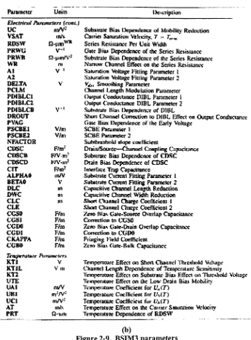
![Figure 3-1. CMOS model describing parasitic diodes [1].](https://thumb-us.123doks.com/thumbv2/123dok_us/124046.12020/39.506.55.451.56.266/figure-cmos-model-describing-parasitic-diodes.webp)
![Figure 4-2. Example of CPL Architecture [9]](https://thumb-us.123doks.com/thumbv2/123dok_us/124046.12020/51.506.81.415.59.263/figure-example-of-cpl-architecture.webp)
![Figure 4-10. Two input NAND power ratio [10]](https://thumb-us.123doks.com/thumbv2/123dok_us/124046.12020/58.506.55.457.229.485/figure-two-input-nand-power-ratio.webp)
![Figure 4-12. Elmore delay model [37]](https://thumb-us.123doks.com/thumbv2/123dok_us/124046.12020/60.506.39.334.316.586/figure-elmore-delay-model.webp)
![Figure 4-14. Power consumption is not always minimized with device size minimizing [13]](https://thumb-us.123doks.com/thumbv2/123dok_us/124046.12020/63.506.82.415.186.432/figure-power-consumption-minimized-device-size-minimizing.webp)
![Figure 5-1. Example of a floor plan [14]](https://thumb-us.123doks.com/thumbv2/123dok_us/124046.12020/68.506.55.455.56.461/figure-example-of-a-floor-plan.webp)
![Figure 5-2a. Methodology 1 [14]](https://thumb-us.123doks.com/thumbv2/123dok_us/124046.12020/71.507.114.280.378.652/figure-a-methodology.webp)
![Figure 5-3a. Methodology 2 [14]](https://thumb-us.123doks.com/thumbv2/123dok_us/124046.12020/72.506.152.349.218.516/figure-a-methodology.webp)
![Figure 5-3b. Design strategy 2 [14]](https://thumb-us.123doks.com/thumbv2/123dok_us/124046.12020/73.506.159.345.56.290/figure-b-design-strategy.webp)