Iowa State University Patents
Iowa State University Research Foundation, Inc.
8-12-2010
Pb-Free Sn-Ag-Cu-Mn Solder
Iver E. Anderson
Iowa State University
, [email protected]
Joel Harringa
Iowa State University
Jason K. Walleser
Follow this and additional works at:
http://lib.dr.iastate.edu/patents
Part of the
Materials Science and Engineering Commons
This Patent Application is brought to you for free and open access by the Iowa State University Research Foundation, Inc. at Iowa State University Digital Repository. It has been accepted for inclusion in Iowa State University Patents by an authorized administrator of Iowa State University Digital Repository. For more information, please [email protected].
Recommended Citation
Anderson, Iver E.; Harringa, Joel; and Walleser, Jason K., "Pb-Free Sn-Ag-Cu-Mn Solder" (2010).Iowa State University Patents. 80.
Pb-Free Sn-Ag-Cu-Mn Solder
Abstract
A solder alloy comprises Sn, Ag, Cu, and Mn and has a melting temperature of about 211 degrees C. A solder
joint and solder process embody the solder alloy as well as solder balls and solder paste made therefrom to
provide a solidified joint that includes three different intermetallic phases and a Sn metal phase. An exemplary
Sn—Ag—Cu—Mn alloy consists essentially of about 3 to about 4 weight % Ag, about 0.80 to about 1.0
weight % Cu, and about 0.05 to about 0.15 weight % Mn, and balance consisting essentially of Sn.
Keywords
Ames Laboratory, Materials Science and Engineering
Disciplines
Materials Science and Engineering
US 20100203353A1
(19) United States
(12) Patent Application Publication (10) Pub. No.: US 2010/0203353 A1
Anderson et al.
(43) Pub. Date:
Aug. 12, 2010
(54)
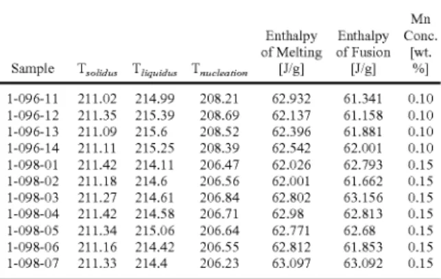
(75)
(73)
(21)
(22)
(60)
PB-FREE SN-AG-CU-MN SOLDER
Inventors: Iver E. Anderson, Ames, IA (U S);
Joel Harringa, Ames, IA (US);
Jason K. Walleser, Idaho Falls, IA
(Us)
Correspondence Address:
Edward J. Timmer
Suite 205, 121 East Front Street
Traverse City, MI 49684 (US)
Assignee: Iowa State University Research Foundation, Inc.
Appl. No.:
12/456,853
Filed: Jun. 23, 2009 Related U.S. Application Data
Provisional application No. 61/207,015, ?led on Feb.
6,2009.
Publication Classi?cation
(51) Int. Cl.
B32B 15/01 (2006.01)
C22C 13/00 (2006.01)
(52) U.S. Cl. ... .. 428/646; 420/560; 428/615; 228/101;
420/591
(57)
ABSTRACT
A solder alloy comprises Sn, Ag, Cu, and Mn and has a melting temperature of about 211 degrees C. A solder joint
and solder process embody the solder alloy as Well as solder balls and solder paste made therefrom to provide a solidi?ed joint that includes three different intermetallic phases and a
Sn metal phase. An exemplary SniAgiCuiMn alloy con
sists essentially of about 3 to about 4 Weight % Ag, about 0.80 to about 1.0 Weight % Cu, and about 0.05 to about 0.15 Weight
Patent Application Publication
Aug. 12, 2010 Sheet 2 0f 6
US 2010/0203353 A1
300 *
Heat Flow, Ends Up
[mW]
20?.’
213$
120$
L208
210
212
‘214
216
Temperature [°C]
Patent Application Publication
Aug. 12, 2010 Sheet 4 0f 6
US 2010/0203353 A1
Heat Flow, Endo Up
[mW]
h 1 l V“;- l
210
211
212
213
214
215
216
217 v
218
Patent Application Publication
Aug. 12, 2010 Sheet 5 0f 6
US 2010/0203353 A1
iiiiii?é?
{3% 2 m ‘I; ‘z mm
Patent Application Publication
Aug. 12, 2010 Sheet 6 0f 6
US 2010/0203353 A1
US 2010/0203353 A1
PB-FREE SN-AG-CU-MN SOLDER
RELATED APPLICATION
[0001] This application claims priority and bene?ts of US. provisional application Ser. No. 61/207,015 ?led Feb. 6, 2009, the disclosure of Which is incorporated herein by ref
erence.
CONTRACTUAL ORIGIN OF THE INVENTION
[0002] This invention Was made With government support under Contract No. DE-ACO2-07CH11358 aWarded by the
US. Department of Energy. The government has certain rights in the invention.
FIELD OF THE INVENTION
[0003] The present invention provides a Pb-free solder
alloy (SniAg4CuiMn) that displays an unexpectedly loW
melting point (about 2110 C.) and minimal melting range
(<about 6° C.), indicative of a quaternary eutectic and can be used as a loW melting Pb-free solder alloy for joining elec
tronic assemblies and electrical contacts and to substitute for Pb-containing solders in all surface mount solder assembly operations, including solder paste re?oW and ball grid array
joints.
BACKGROUND OF THE INVENTION
[0004] The global electronic assembly community is striv
ing to accommodate the replacement of Pb-containing sol
ders, primarily SniPb alloys, With Pb-free solders due to
environmental regulations and market pres sures. During this major transition aWay from eutectic or near-eutectic SniPb
solder (Tem_:183o C.) for electronic assembly, there is also the opportunity to make a major improvement in Pb-free joint
reliability for challenging operating environments, i.e., high
temperatures and stress levels, as Well as impact loading situations. Of the Pb-free choices, an array of solder alloys
based on the Sn-3.7%Ag-0.9% Cu (in Wt. %) ternary eutectic
(Tem_:217o C.) composition (known as SAC3709) have
emerged With the most potential for broad use across the industry. US. Pat. No. 5,527,628 describes such Pb-free sol
der alloys.
[0005] An observation that arose from initial Widespread
testing of SniAgiCu (SAC) solder alloys Was the occa
sional embrittlement of SAC solder joints due to micro-void
nucleation, groWth, and coalescence, if the exposure to
elevated temperatures Was suf?ciently high, typically greater
than about 150° C., and the exposure Was suf?ciently long,
greater than about 500 to 1000 h (hours). This occasional joint
embrittlement after thermal aging Was observed at elevated Cu content in SAC solder alloys and typically Was associated With excessive groWth of layers of Cu-base intermetallic com
pounds, Cu6Sn5 and, especially, Cu3Sn. It should be noted
that US. Pat. No. 6,231,691 provides a solder to suppress this
thermal aging phenomenon through minor additions (<1 Wt.
%, but usually 0.2-0.3 Wt. %) of a fourth element, such as Ni,
Fe, and/or Co, and “like-acting elements,” to the SAC solder to suppress solid state diffusion at the solder/substrate inter face that contains the Cu-base intermetallic compound layers.
Later testing (see reference A) shoWed that a 0.3 Wt. % Mn
substitutional addition to SAC3709 Was one of the most effec
tive like-acting elemental additions, suppressing groWth of
both types of intermetallic layers after extensive thermal aging. This type of minor alloy addition to prevent embrittle
Aug. 12, 2010
ment has become increasingly important since narroW solder
joint gaps are becoming more common With miniaturization
of electronic circuits. (Reference Ail. E. Anderson and J. L.
Harring a, “Suppression of Void Coalescence in Thermal Aging of Tin-Silver-Copper-X Solder Joints,” J. Elec. Mater.
(2006), Vol. 35 (1), p. 1-13).
[0006] Studies have shoWn that Sn dendrites Were the dominant as-solidi?ed microstructure feature in solder joints made With many SAC alloys, not a ?ne (ternary) eutectic,
contrary to the previous experience With SniPb. Also, it Was found that relatively high but variable undercooling Was observed commonly before joint solidi?cation, leading to Sn dendrites With spacing variations (that depend on undercool ing and groWth rate) but With very feW distinct Sn grains. The unusually high undercooling of the SAC solder joints Was associated With the dif?culty of nucleating Sn solidi?cation,
as a pro-eutectic phase. Especially during sloW cooling, e. g.,
in ball grid array (BGA) joints, increased undercooling of the joints also can promote formation of undesirable pro-eutectic intermetallic phases, speci?cally Ag3 Sn “blades,” that tend to
coarsen radically, leading to embrittlement of as-solidi?ed
solder joints.
[0007] References 1, 2, 3, and 4 listed beloW employed
fourth element additions to SAC solders With the intention of
avoiding Ag3Sn blades by selecting SAC compositions that
Were de?cient in Ag and Cu, e.g., see SAC2705 [see ref 4],
SAC305, and SAC105 [see refs. 1, 2, 3]. These references include the folloWing:
[0008] l. W. Liu and N-C. Lee, “The Effects ofAdditives to SnAgCu Alloys on Microstructure and Drop Impact Reli ability of Solder Joints,” JOM, 59, no. 7 (2007) pp. 26-31. [0009] 2. L-W. Lin et al., “Alloying modi?cation of SniAg4Cu solders by manganese and titanium,” Micro
electron. Reliab. (2008), doi:10.1016/j.microrel.2008.10.
001.
[0010] 3. W. Liu, P. Bachorik, and N-C. Lee, “The Superior
Drop Test Performance of SAC-Ti Solders and Its’ Mecha
nism,” Proc 58”’ Electronic Components and Technology
Conf, (2008), pp. 627-635.
[0011] 4. S. K. Kang, P. A. Lauro, D.-Y. Shih, D. W. Hend
erson, K. J. PuttlitZ, IBM J. Res. Dev. 49(4/5), 607-620
(2005).
[0012] In these references, some marginally near-eutectic
SAC alloy designs Were proposed With a loW Cu level (0.5%)
and very loW Ag levels, less than 2.7% Ag [ref. 4] and doWn
to 1% Ag (SAC105). These base alloys Were selected since they Would tend to promote Sn formation and inhibit nucle
ation of Ag3Sn [ref. 1, 2, 3, 4]. Because these alloys deviate
increasingly from the eutectic, they exhibit a Wider melting
range (mushy Zone) With a liquidus temperature (for
SAC105) as high as 2260 C. Unfortunately, some observa tions of unmodi?ed SAC105 interfacial failure on impact
loading still occurred, since occasional high undercooling
still may permit Ag3 Sn blade formation during sloW cooling.
These “interfacial adhesion” failures prompted attempts at alloy modi?cations of SAC105 solder With 1-2 additions
[refs. 1, 2] to improve impact resistance of BGA joints by
increasing the interfacial bond strength of the intermetallic
layer and, presumably, by suppressing Ag3Sn blade forma
tion. While signi?cant improvement in impact resistance Was observed, especially for SAC105+0.13Mn and SAC105+0. 02Ti alloys [ref. 3] (and no Ag3 Sn blades Were reported), their
US 2010/0203353 A1
mushy Zone (equal to 9° C. because of the 2170 C. solidus
temperature) inhibits broad service application.
SUMMARY OF THE INVENTION
[0013] In an embodiment, the present invention provides an
alloy comprising Sn, Ag, Cu, and Mn and having a melting
temperature of about 21 1 degrees C., Which is Well beloW the melting temperature of other SAC solder alloys. The alloy typically exhibits a liquid plus solid temperature range of less than about 6 degrees C., often less than about 4 degrees C.
[0014] An illustrative embodiment of the invention pro
vides a Pb-free solder alloy consisting essentially of about 3
to about 4 Weight % Ag, about 0.80 to about 1.0 Weight % Cu, and about 0.05 to about 0.15 Weight % Mn, and balance
consisting essentially of Sn.
[0015] Another illustrative embodiment of the invention
provides a Pb-free solder alloy consisting essentially of about 3 to about 4 Weight % Ag, 0.95-y Weight % Cu, and y Weight
% Mn and balance consisting essentially of Sn Wherein y is about 0.05 to about 0.15 Weight %.
[0016] A further illustrative embodiment of the invention
provides a Pb-free solder alloy comprising Sn, Ag, Cu, and
Mn and having four different phases including three different intermetallic phases and a Sn metal phase. For example, the intermetallic phases include a phase comprising Sn and Mn
(probably MnSn2), Cu6Sn5 phase, and Ag3Sn phase.
[0017] The present invention also provides a solder joint and solder process that embody a SniAg4CuiMn alloy of the type discussed above. The solder joint has a microstruc ture having four different phases including three different intermetallic phases and a Sn metal phase. For example, the intermetallic phases include a phase comprising Sn and Mn
(probably MnSn2), Cu6Sn5 phase, and Ag3Sn phase. The Sn
metal phase typically is [3-Sn phase. The solder joint is formed
by the solder being solidi?ed on an electrical Wiring board and/or about copper electrical conductors in illustrative embodiments of the invention.
[0018] The solder joints made With the neW SniAgi CuiMn (Pb-free) solder alloy may need to accommodate
some minor addition of Pb due to re?oW and mixing With
SniPb component lead plating during re?oW assembly of
solder joints. Slight contamination by such small Pb levels is not expected to raise the bene?cial (about 211 degrees C.) melting point of the neW SniAgiCuiMn solder alloys and may even help improve the Wettability during joint for
mation. This type of Pb -tolerant behavior is an advantage over
competing SniAgiBi (Pb -free) solders that run the risk of generating an extremely loW melting SniPbiBi ternary eutectic, if alloyed With SniPb component platings. It is expected that the global supply of “legacy” electronic com
ponents With SniPb solder plating Will continue to diminish and eventually vanish during the current transition to full
Pb-free electronic soldering, but this possibility must be tol erated in any neW Pb-free solders that are proposed.
[0019] The SniAg4CuiMn (SACM) solder alloy
exhibits the signi?cantly reduced melting point (melting tem
perature) of about 211 degrees C. as compared to the melting
points of SAC ternary eutectic solder (217 degrees C.), the
SniAg binary eutectic solder (221 degrees C.), and the
Sn4Cu binary eutectic solder (227 degrees C.). This signi?
cantly reduced melting point is a great advantage for solder assembly of electronic circuits and electrical systems. In the type of solder paste re?oW and ball grid array (BGA) appli cations that are envisioned for use With the SACM solder,
Aug. 12, 2010
every single degree of reduced re?oW temperature is a pre
cious advantage for reducing damage to temperature sensitive
electronic components and to the circuit board material,
itself. In fact, a reason that SAC solder came into broad use as
a Pb-free alternative to SniPb solder is that the minimum
re?oW temperature of SAC solder for most applications,
about 240 degrees C., is just beloW the threshold for signi?
cant damage of one of the most popular circuit board mate
rials, a ?berglass/epoxy composite, i.e., FR-4. Thus, the SACM solder alloy pursuant to the present invention should
permit a more comfortable margin for preventing thermal damage of most components and common circuit board mate rials.
[0020] It should also be mentioned that the use of the
SACM solder alloy balls (e.g. spheres) according to an
embodiment of the invention for BGA applications may also
involve the use of a small deposit of a solder paste With a different composition, typically a SAC305 solder paste referred to above. The function of this paste is to cause adher ence of each solder ball to the proper spot on the conductor array pattern during handling to prepare for re?oW. During heating in the re?oW operation With the SAC305 solder paste,
for example, each SACM solder ball Will melt ?rst at about 211 degrees C. before the paste deposit starts to melt at 217
degrees C. During further heating to complete the re?oW
operation some alloying of the SACM solder ball Will occur While both solder components are molten above 217 degrees
C. that may cause a composition gradient or some minor
dilution of the Mn in the interfacial region of the substrate. HoWever, the relative volume of each SACM solder ball nor
mally is overWhelming relative to its corresponding paste
deposit and the bene?cial effect of the initial Mn content of each SACM solder ball on promoting BGA joint solidi?ca
tion With loW undercooling and suppression of Ag3 Sn blades
is not expected to diminish.
[0021] The above advantages of the invention Will become more readily apparent from the folloWing detailed description
taken With the folloWing draWings.
BRIEF DESCRIPTION OF THE DRAWINGS
[0022] FIG. 1 illustrates solder joint undercooling results for the base SAC3595 solder (Sn-3.5% Ag-0.95% Cu- % by Weight) and as a function of concentration of X addition for
the solder alloy Where XIMn addition to the base SAC3595
solder alloy for DSC (differential scanning calorimetry) mea surements at 0.170 C./ sec cooling rate.
[0023] FIG. 2 shoWs a summary of DSC results for
SAC3595+0.10Mn solderjoints (i.e. 0.10 Wt. % Mn).
[0024] FIG. 3 is a typical SEM micrograph (scanning elec
tron micrograph) of a SAC3595+0.10 Wt. % Mn solder joint. [0025] FIG. 4 shoWs a summary of an expanded region of the heating ther'mo grams for the three Mn concentration lev
els tested (0.05%, 0.10%, 0.15% by Weight Mn) as substitu tional additions (for Cu) to SAC3595.
[0026] FIG. 5 is a SEM micrograph of the matrix region of
a solder joint made With SAC3595+0.10Mn, shoWing the
MnSn2 intermetallic compound phases in the Sn metal phase.
US 2010/0203353 A1
blocks (2.5><2.5><0.5 cm) at a peak re?oW temperature of 2350
C. (FIG. 6a) and 2550 C. (FIG. 6b).
DETAILED DESCRIPTION OF THE INVENTION
[0028] The present invention involves reducing the unusu
ally high undercooling of SAC (SniAgiCu) solder joints
described above, Where there can be dif?culty in nucleating Sn solidi?cation as a pro-eutectic phase, especially during sloW cooling, such as existing for ball grid array (BGA) joints. As mentioned above, increased undercooling of the
solder joints can promote formation of undesirable pro-eu
tectic intermetallic phases, speci?cally Ag3Sn “blades,” that
tend to coarsen radically, leading to embrittlement of as solidi?ed solder joints.
[0029] In an embodiment of the present invention, a qua
ternary alloy is provided comprising Sn, Ag, Cu, and Mn
Wherein the alloy composition exhibits a melting temperature of about 211 degrees C., Which is Well beloW the melting temperature of other SAC solder alloys. The quaternary
SniAg4CuiMn
alloy typically exhibits a liquid plus solid
temperature range of less than about 6 degrees C., often less than about 4 degrees C. Other alloying elements may be present in the solder alloy that do not substantially affect the
melting temperature thereof.
[0030] An illustrative embodiment of the invention pro
vides a Pb-free solder alloy consisting essentially of about 3
to about 4 Weight % Ag, about 0.80 to about 1.0 Weight % Cu, and about 0.05 to about 0.15 Weight % Mn, and balance
consisting essentially of Sn.
[0031] Another illustrative embodiment of the invention
provides a Pb-free solder alloy consisting essentially of about 3 to about 4 Weight % Ag, 0.95-y Weight % Cu, and y Weight
% Mn and balance consisting essentially of Sn Wherein y is about 0.05 to about 0.15 Weight %.
[0032] A still further illustrative embodiment of the inven
tion provides a Pb-free solder alloy comprising Sn, Ag, Cu,
and Mn and having four different phases including three
different intermetallic phases and a Sn metal phase. For
example, the intermetallic phases include a phase comprising
Sn and Mn (probably MnSn2), Cu6Sn5 phase, and Ag3Sn
phase.
[0033] For purposes of further illustrating the invention Without limiting it, the present invention is described beloW
With respect to modifying a near-eutectic alloy, SAC3595
solder alloy (Sn-3.5% Ag-0.95% Cu, in Weight %) as a base by alloying With a fourth element, Mn (manganese) to reduce undercooling of solder joints. In modifying base SAC3595
solder alloy, Mn Was alloyed With the base solder alloy to
promote nucleation of pro-eutectic Cu6Sn5 Within the solder
joint matrix (liquid alloy) in addition to its formation on the substrate interface, providing additional interfacial area for Sn nucleation. Also, the Mn addition promotes formation of a
SniMn intermetallic phase (probably MnSn2) that may
enhance heterogeneous nucleation of Sn. The Mn addition also may strain the lattice of the Cu6Sn5 phase, in both pro eutectic and interfacial layer phases, to make a more potent
epitaxial nucleation catalyst for Sn, thus reducing the joint
undercooling and the potential to form Ag3Sn blades,
although applicants do not intend or Wish to be bound by any
theory in this regard.
[0034] The bulk undercooling measurements for the solder
joints made from the SAC3595+Mn alloys that Were selected (i.e. Mn:0.05%, 0.10% and 0.15% by Weight) are summa riZed in FIG. 1. For each Mn concentration level tested, at
Aug. 12, 2010
least 7 repeated trials Were used. Inspection shoWs that the Mn addition is an active catalytic addition since these concentra tions of Mn have relatively loWer undercooling values as
compared to the average undercooling of unmodi?ed SAC3595 base solder alloy. The range of undercooling values
for unmodi?ed SAC3595 is indicated in FIG. 1 by the left hand bar at the Zero concentration, With the data spread indi
cated by the bracket. Mn can be seen to have a potent and
consistent nucleation effect. Note that the nucleation tem perature (Tmm) is de?ned as the onset point of the exothermic
crystallization peak in each DSC thermogram, consistent
With the literature in this ?eld. Also, the bulk undercooling,
AT, is de?ned at the difference betWeen the onset of melting at the solidus temperature (T501) and the onset of nucleation, i.e., ATITSOFTMC. Also note that observation on heating in a
differential scanning calorimeter (DSC) of the solidus tem
perature for a eutectic alloy is also the singular eutectic melt
ing point, Tel”, and not just the start of a melting range betWeen solidus and liquidus temperatures. The DSC appa ratus used Was a Pyris 1 poWer compensating DSC available
from Perkin-Elmer.
[0035] Importantly, the calorimetric results for the Mn
addition to the SAC3595 base solder alloy shoW a very potent effect on suppressing undercooling, FIG. 1, and are also cor
related or indexed to a neW loWer melting onset (solidus temperature) of about 211 degrees C., shoWn in Table 1 for Mn additions of 0.05%, 0.10% and 0.15% by Weight for alloys in accordance With the present invention. As speci?c
evidence of the consistency of the observations from the calorimetric results for the Mn additions to SAC3595, Table 1
gives a complete summary of the melting and solidi?cation observations. The depression of the melting temperature to
about 21 1 degrees C. is unique for the Mn-modi?ed alloys as compared to calorimetry data for SAC3595, Which exhibits a
consistent solidus temperature of 217 degrees C.
[0036] Furthermore, a comparison to other undercooling data published for SAC105 and SAC105+Mn [see reference
1] revealed an essentially consistent solidus temperature that varies from a minimum of217. 13 degrees C. (for Sn-1.07Ag 0.47Cu-0.085Mn) to a maximum of 217.81 degrees C. (for Sn-1 .13Ag-0.6Cu-0.16Mn). Other results from this reference for SAC+Mn alloys With higher levels of Ag and Cu reveal a
solidus temperature of 217.18 degrees C. (for Sn-1.76Ag-0.
68Cu-0.15Mn) and of 217.43 degrees C. (for Sn-2.59Ag-0.
65Cu-0.12Mn). An alloy of Sn-1.0Ag-0.46Cu-0.3 Bi-0.0.
1Mn exhibited a slightly reduced solidus temperature of 21 6.
22 degrees C., but it had a Bi addition as Well as Mn.
TABLE 1
Summary ofDSC Results for Mn Additions to SAC3595
Mn
Enthalpy Enthalpy Cone.
of Melting of Fusion [Wt.
US 2010/0203353 A1
TABLE l-continued
Summary ofDSC Results for Mn Additions to SAC3595
Mn
Enthalpy Enthalpy Cone.
of Melting of Fusion [Wt.
53mph? Tsolidus Tliquidus Tnuclean'on l-l/gl l-l/gl %l 1-096-11 211.02 214.99 208.21 62.932 61.341 0.10 1-096-12 211.35 215.39 208.69 62.137 61.158 0.10 1-096-13 211.09 215.6 208.52 62.396 61.881 0.10 1-096-14 211.11 215.25 208.39 62.542 62.001 0.10 1-098-01 211.42 214.11 206.47 62.026 62.793 0.15 1-098-02 211.18 214.6 206.56 62.001 61.662 0.15 1-098-03 211.27 214.61 206.84 62.802 63.156 0.15 1-098-04 211.42 214.58 206.71 62.98 62.813 0.15 1-098-05 211.34 215.06 206.64 62.771 62.68 0.15 1-098-06 211.16 214.42 206.55 62.812 61.853 0.15 1-098-07 211.33 214.4 206.23 63.097 63.092 0.15
[0037] Referring to FIG. 2, the newly discovered solidus temperature of about 211 degree C. can be seen as the initial
(upward) deviation from the baseline on heating to start the
endothermic peak that represents solder joint melting in the
DSC thermogram results summary in FIG. 2 for the SAC3595+0.10Mn alloy in accordance With the invention.
Although not shoWn in FIG. 2, the heating baseline continues
up to the peak re?oW temperature of 240 degrees C. in these
experiments Without any other endothermic signals, consis tent With the apparent completion of melting (liquidus tem perature) at 214-215 degrees C., as recorded in Table 1. An
SEM micrograph in FIG. 3 shoWs an example of one of the SAC3595+0.10Mn solder joints that solidi?ed on cooling in
one of the thermo grams in FIG. 2, Where the Cu substrates are
shoWn on the top and bottom of the micrograph in dark
contrast.
[0038] Moreover, the heating thermograms for the solder
joints made from the three SAC3595+Mn alloy samples in
accordance With the invention that Were studied all display the same consistent melting onset temperature (solidus tem perature) of about 21 1 degrees C. as shoWn in the summary of
FIG. 4. HoWever, each alloy thermogram in FIG. 4 shoWs some evidence for multiple (overlapping) endothermic peaks. Because of the signi?cant depression of the melting onset by
about 6 degrees C. beloW the normal Sn-3.5% Ag-0.95% Cu
ternary eutectic temperature (nominally 217 degrees C.) by
the substitutional addition of only 0.05 Wt. % Mn into
SAC3595 (Sn-3.5Ag-0.90Cu-0.05Mn), a neW quaternary (perhaps a quaternary eutectic) solder alloy has been discov
ered in accordance With the invention. While undercooling
can cause the solidi?cation reaction to occur over a range of
temperatures, the melting of a quaternary “eutectic” alloy should occur theoretically at a singular temperature, like a
pure metal. From a comparison of the endothermic peak
shapes of the three alloys in FIG. 3, it is thought that the
quaternary (perhaps quaternary eutectic) alloy composition is
probably closest to Sn-3.5% Ag-0.85% Cu-0.10% Mn (in
Weight %), termed SAC3595+0.10Mn, since these peaks
seem to be the most singular and to have the narroWest appar
ent melting range. This observation can be con?rmed by a
series of melting and solidi?cation studies at sloWer heating (and cooling) rates. The SAC3595+0.10Mn alloy neverthe less is a preferred representative of the neWly discovered
quaternary solder in accordance With the invention.
[0039] Another veri?cation of this quaternary (perhaps
quaternary eutectic) solder alloy must come from the identi
Aug. 12, 2010
?cation of an additional phase in the solidi?ed microstructure of these solder joints, since a quaternary eutectic reaction
must have four product phases that solidify from a single phase alloy liquid. FIG. 5 provides an SEM micrograph of the
solder matrix region of a SAC3595+0.10Mn joint similar to that in FIG. 3, but at a higher magni?cation and after ion
surface etching. In this microstructure, the quaternary eutec
tic Was found to be composed of [3-Sn, Cu6Sn5, Ag3Sn, and a
Mn-containing compound (probably MnSn2). Wavelength
dispersive spectroscopy (WDS) analysis shoWs that all of the
?rst three phases ([3-Sn, Cu6Sn5, Ag3Sn) are present, along
With a SniMn compound (probably MnSn2) With up to about 27 at. % Mn. Unfortunately, the SniMn micron siZed particles (circled on the micrograph) are too small for high precision quantitative WDS measurement due to their siZe relative to the electron-specimen interaction volume. HoW
ever, the phase diagram for the MniSn system alloWs esti mation that MnSn2 is the closest phase corresponding to the WDS measurements. The presence of this fourth SniMn phase combined With the reduced liquidus and solidus tem peratures are strong evidence that a neW quaternary eutectic
solder has been discovered pursuant to the invention.
[0040] The reduced melting temperature of SACM solder
pursuant to the invention is a great advantage, as described above. To evaluate solderability of the SACM solder, macro
scopic solder joints of SAC3595+0.10Mn Were produced in
ambient air at a reduced re?oW temperature of 235 degrees C. (see FIG. 6a) and at an elevated re?oW temperature of 255
degrees C. (FIG. 6b) to check for the ability to penetrate a long narroW joint gap and to Wet the surface of the Cu substrates.
FIGS. 6a and 6b illustrate the effects of temperature on this
SACM solder surface, With the FIG. 6a joint produced at 235 degrees C. having some reduction in the golden oxide color,
compared to the same solder used to prepare the FIG. 6b joint
at 255 degrees C. While the Wetting angle of the surface solder
puddle for both conditions does not look to be much less than
90 degrees, a common de?nition for acceptable solder Wet tability, sectioning of the solder j oints shoWed that the interior
gap Was completely Wetted and ?lled for both. Thus, this is an indication of suf?cient solderability, even in open air, Which is
desirable for manufacturing simplicity.
[0041] The present invention thus provides a solder joint and solder process that embody the SACM (Sn.Sg4Cui Mn) alloy. The solder joint has a microstructure having four different phases including three different intermetallic phases, such as the Cu6Sn5 phase, Ag3 Sn phase, and SniMn
phase (probably MnSn2), together With the Sn metal phase,
i.e. [3-Sn phase. The solder joint is formed by the solder being
solidi?ed on an electrical Wiring board about copper electri
cal conductors thereof in illustrative embodiments of the
invention. The solder can be incorporated into an electronic
solder paste and used for circuit assembly to this end.
[0042] The SniAgiCuiMn
(SACM) solder alloy of the
present invention is advantageous in that the alloy exhibits the
signi?cantly reduced melting point (melting temperature) of
about 211 degrees C. as compared to the melting points of
SAC ternary eutectic solder (217 degrees C.), the SniAg
binary eutectic solder (221 degrees C.), and the Sn4Cu
binary eutectic solder (227 degrees C.). This signi?cantly
reduced melting point is a great advantage for solder assem
bly of electronic circuits and electrical systems. In the type of
solder paste re?oW and ball grid array applications that are envisioned for use With the SACM solder, every single degree
US 2010/0203353 A1
reducing damage to temperature sensitive electronic compo nents and to the circuit board material, itself. In fact, a reason
that SAC solder came into broad use as a Pb-free alternative
to SniPb solder is that the minimum re?oW temperature of
SAC solder for most applications, about 240 degrees C., is just beloW the threshold for signi?cant damage of one of the
most popular circuit board materials, a ?berglass/epoxy com
posite, i.e., FR-4. Thus, the SACM solder alloy pursuant to the present invention should permit a more comfortable mar gin for preventing thermal damage of most components and common circuit board materials. For use in solder paste re?oW and ball grid array applications, the invention envi sions providing solder balls, such as substantially solder spheres or near-spheres, comprising the invention solder
alloy in a solder ball siZe range of about 100 microns to 1000 microns diameter for purposes of illustration and not limita tion.
[0043] The SniAgiCuiMn
(SACM) solder alloy of the
present invention should be useful for loW temperature re?oW of Pb-free solderpaste and BGA balls (e.g. spheres) as Well as
other soldering applications.
[0044] Another important advantage of the SACM solder pursuant to the invention involves reduction or avoidance of the formation of Ag3 Sn blades in the as-solidi?ed solder joint microstructure. Analysis of all of the solder joint samples for the full range of Mn additions revealed that a minimum of 0.10% by Weight Mn appears to completely suppress Ag3 Sn
blade phase formation, even at the sloW cooling rate that is common for BGA assembly. This high level of control of the
solder joint microstructure should produce superior results in
board level impact conditions, but this also remains to be
veri?ed by such full scale testing.
[0045] While the invention has been described in terms of speci?c embodiments thereof, those skilled in the art Will appreciate that modi?cations and changes can be made thereto Within the scope of the appended claims.
1. An alloy comprising Sn, Ag, Cu, and Mn and having a melting temperature of about 211 degrees C.
2. The alloy of claim 1 having a liquid plus solid tempera
ture range less than about 6 degrees C.
3. The alloy of claim 1 having three different intermetallic
phases and a Sn metal phase.
4. The alloy of claim 3 Wherein the intermetallic phases
include a phase comprising Sn and Mn.
5. The alloy of claim 4 Wherein the phase is MnSn2. 6. The alloy of claim 3 Wherein other intermetallic phases
include Cu6Sn5, and Ag3Sn.
7. An alloy consisting essentially of about 3 to about 4 Weight % Ag, about 0.80 to about 1.0 Weight % Cu, and about 0.05 to about 0.15 Weight % Mn, and balance consisting essentially of Sn.
8. The alloy of claim 7 including at least about 0.10 Weight % Mn.
9. An alloy consisting essentially of about 3 to about 4 Weight % Ag, 0.95-y Weight % Cu, and y Weight % Mn and
balance consisting essentially of Sn Wherein y is about 0.05 to
about 0.15 Weight %.
10. The alloy of claim 9 including at least about 0.10
Weight % Mn.
11. An alloy comprising Sn, Ag, Cu, and Mn and having
three different intermetallic phases and a Sn metal phase.
12. The alloy of claim 11 Wherein the intermetallic phases
include a phase comprising Sn and Mn.
Aug. 12, 2010
13. A solder joint comprising a Pb-free solder solidi?ed in
contact With an electrical conductor Wherein said solder com prises Sn, Ag, Cu, and Mn and has a melting temperature of about 211 degrees C.
14. The joint of claim 13 having three different intermetal
lic phases and a Sn metal phase.
15. The joint of claim 13 Wherein the intermetallic phases
include a phase comprising Sn and Mn.
16. The joint of claim 15 Wherein the phase comprises
MnSn2.
17. The joint of claim 13 Wherein other intermetallic
phases include Cu6Sn5, and Ag3Sn.
18. The joint of claim 13 formed on an electrical Wiring board.
19. The joint of claim 13 formed about copper electrical conductors.
20. A solder joint comprising a Pb-free solder solidi?ed in
contact With an electrical conductor Wherein said joint con
sists essentially of about 3 to about 4 Weight % Ag, about 0.80 to about 1.0 Weight % Cu, and about 0.05 to about 0.15 Weight
% Mn, and balance consisting essentially of Sn.
21. The joint of claim 20 including at least about 0.10
Weight % Mn.
22. The joint of claim 20 formed on an electrical Wiring board.
23. The joint of claim 20 formed about copper electrical conductors.
24. A solder joint comprising a Pb-free solder solidi?ed in contact With an electrical conductor Wherein the joint consists
essentially of about 3 to about 4 Weight % Ag, 0.95-y Weight % Cu, and y Weight % Mn and balance consisting essentially
of Sn Wherein Mn is about 0.05 to about 0.15 Weight %. 25. The joint of claim 24 including at least about 0.10
Weight % Mn.
26. The joint of claim 24 formed on an electrical Wiring board.
27. The joint of claim 24 formed about copper electrical conductors.
28. A solder joint comprising a Pb-free solder solidi?ed in
contact With an electrical conductor Wherein the joint com prises Sn, Ag, Cu, and Mn and includes three intermetallic
phases and a Sn metal phase.
29. The joint of claim 28 formed on an electrical Wiring board.
30. The joint of claim 28 formed about copper electrical conductors.
31. In a soldering process, the step of solidifying a molten
Pb-free solder comprising Sn, Ag, Cu, and Mn and having a melting temperature of about 211 degrees C.
32. The process of claim 31 Wherein the solder is solidi?ed
on an electrical Wiring board.
33. The process of claim 31 Wherein the solder is solidi?ed about copper electrical conductors.
34. In a soldering process, the step of solidifying a molten Pb-free solder consisting essentially of about 3 to about 4
Weight %Ag, about 0.80 to about 1.0 Weight % Cu, and about 0.05 to about 0.15 Weight % Mn, and balance consisting essentially of Sn.
35. The process of claim 34 Wherein the solder includes at least about 0.10 Weight % Mn.
36. The process of claim 34 Wherein the solder is solidi?ed
on an electrical Wiring board.
US 2010/0203353 A1
38. In a solder process, the step of solidifying a molten
Pb-free solder consisting essentially of about 3 to about 4
Weight % Ag, 0.95-y Weight % Cu, and y Weight % Mn and balance consisting essentially of Sn Wherein Mn is about 0.05
to about 0.15 Weight %.
39. The process of claim 38 Wherein the solder includes at least about 0.10 Weight % Mn.
40. The process of claim 38 Wherein the solder is solidi?ed
on an electrical Wiring board.
41. The process of claim 38 Wherein the solder is solidi?ed about copper electrical conductors.
42. In a solder process, the step of solidifying a molten
Pb-free solder comprising Sn, Ag, Cu, and Mn in a manner that the solidi?ed solder microstructure includes three inter metallic phases and a Sn metal phase.
43. The process of claim 42 Wherein one intermetallic phase comprises Sn and Mn
44. The process of claim 43 Wherein the phase comprises
MnSn2.
45. The process of claim 42 Wherein the solder is solidi?ed
on an electrical Wiring board.
46. The process of claim 42 Wherein the solder is solidi?ed about copper electrical conductors.
47. A solder ball comprising an alloy comprising Sn, Ag, Cu, and Mn and having a melting temperature of about 211
degrees C.
Aug. 12, 2010
48. The solder ball of claim 47 having a liquid plus solid temperature range less than about 6 degrees C.
49. The solder ball of claim 47 having three different inter metallic phases and a Sn metal phase.
50. The solder ball of claim 49 Wherein the intermetallic
phases include a phase comprising Sn and Mn.
51. The solderball of claim 50 Wherein the phase is MnSn2. 52. The solder ball of claim 49 Wherein other intermetallic
phases include Cu6Sn5, and Ag3Sn.
53 . A solder ball comprising an alloy consisting essentially of about 3 to about 4 Weight % Ag, about 0.80 to about 1.0
Weight % Cu, and about 0.05 to about 0.15 Weight % Mn, and balance consisting essentially of Sn.
54. The solder ball of claim 53 including at least about 0.10
Weight % Mn.
55. A solder ball comprising an alloy consisting essentially of about 3 to about 4 Weight % Ag, 0.95-y Weight % Cu, and y Weight % Mn and balance consisting essentially of Sn
Wherein y is about 0.05 to about 0.15 Weight %.
56. The solder ball of claim 55 including at least about 0.10
Weight % Mn.
57. A solder ball comprising an alloy comprising Sn, Ag, Cu, and Mn and having three different intermetallic phases
and a Sn metal phase.
58. The solder ball of claim 57 Wherein the intermetallic
phases include a phase comprising Sn and Mn.