Rochester Institute of Technology
RIT Scholar Works
Theses Thesis/Dissertation Collections
7-2012
A Charge Pump Architecture with High
Power-Efficiency and Low Output Ripple Noise in 0.5 μm
CMOS Process Technology
Primit Modi
Follow this and additional works at:http://scholarworks.rit.edu/theses
This Thesis is brought to you for free and open access by the Thesis/Dissertation Collections at RIT Scholar Works. It has been accepted for inclusion in Theses by an authorized administrator of RIT Scholar Works. For more information, please [email protected].
Recommended Citation
A Charge Pump Architecture with High Power-Efficiency and Low Output Ripple Noise in
0.5 µm CMOS Process Technology
by
Primit Modi
A Thesis Submitted in Partial Fulfillment of the
Requirements for the Degree of
Master of Science
in
Electrical and Microelectronics Engineering
Approved by:
_______________________________________________________________________ Advisor: Dr. Robert J. Bowman
_____________________________________________________________________ Member: Dr. James E. Moon
_____________________________________________________________________ Member: Dr. Karl D. Hirschman
_____________________________________________________________________ Department Head: Dr. Sohail A. Dianat
Department of Electrical and Microelectronics Engineering
Kate Gleason College of Engineering
Rochester Institute of Technology
Rochester, New York
NOTICE OF COPYRIGHT
© 2012
Primit Modi
REPRODUCTION PERMISSION STATEMENT
Permission Granted
TITLE:
“A Charge Pump Architecture with High Power-Efficiency and Low Output Ripple Noise in 0.5 µm CMOS Process Technology”
I, Primit Modi, hereby grant permission to the Wallace Library of the Rochester Institute of Technology to reproduce my thesis in whole or in part. Any reproduction will not be for commercial use or profit.
ELECTRICAL AND MICROELECTRONICS ENGINEERING
ROCHESTER INSTITUTE OF TECHNOLOGY
July 2012
ABSTRACT
Kate Gleason College of Engineering Rochester Institute of Technology
Degree : Master of Science
Program : Electrical and Microelectronics Engineering
Name of Candidate : Primit Modi
Title : A Charge Pump Architecture with High Power-Efficiency and Low
Output Ripple Noise in 0.5 µm CMOS Process Technology
Modern integrated microsystems have several functional blocks which require different voltages to
operate adequately. Charge pump circuits are used to generate different voltage domains for
different functional blocks on large integrated microsystems. Charge pump is an inductorless
DC-DC converter which generates higher positive voltage or lower negative voltage from the applied
reference voltage. The thesis presents a high power-efficiency charge pump architecture with low
output ripple noise in AMI 0.5 µm CMOS process technology. The switching action of the
proposed charge pump architecture is controlled by a dual phase non-overlapping clock system. In
order to achieve high power-efficiency, the power losses due to the leakage currents, the finite
switch resistance and the imperfect charge transfer between the capacitors are taken into
consideration and are minimized by proper switching of the charge transfer switches. The
proposed charge pump can operate over the wide input voltage range varying from 3 V to 7 V with
the power conversion efficiency of 90%. The loading current drive capability of the proposed
ACKNOWLEDGMENT
First and frontmost, I would like to thank God almighty for giving me marvelous
opportunities I have had in my life. To my family, I am grateful for all that you have done for me
throughout the years. To my mother, I am thankful to you for your incessant and unconditional
love and sacrifice. I am feeling blessed and esteemed to have mother like you. To my father, I
thank you for your encouragement and everything that you have done to help me reach where I am
now. To them, I owe all.
I have been favorable to have great teachers throughout my life. I would like to take this
opportunity to convey my earnest appreciation to my advisor Dr. Robert Bowman for his faith in
my abilities and consistent help. Without your encouragement, this work would not have been
possible. I wish you success in all your future undertakings. Dr. Moon, you are an excellent
teacher with awe-inspiring work ethic. I feel beatified to have been your student. Dr. Hirschman, I
am truly grateful to you for solemn feedback, help, and encouragement.
I would like to acknowledge Imre Knausz, Murat Ozbas, Mark Pude, Eric Bohannon, Brian
Mott, Eric Moule, Jeff Lillie, Tom Quattrini, Jeff Waldrop, Brad Mitchell, Clint Meyer. You have
CONTENTS
ABSTRACT……… iiI
TABLE OF CONTENTS……… iv
LIST OF FIGURES………... vii
LIST OF TABLES………. x
CHAPTER 1 Introduction……….……… 1
1.1 Background and Motivation………..………. 1.2 Research Objectives………..……… 1.3 Thesis Organization……….………. References……….. 1 5 5 7 CHAPTER 2 Overview of Existing DC-DC Converter Circuits………... 8
2.1 DC-DC Converter Topologies………..………..
2.1.1. Inductor based DC-DC Converter………
2.1.2. Switched-Capacitor based DC-DC Converter……….
(A) Charge Pump Topologies………..
(B) Unregulated and Regulated Charge Pump Topologies………….
References………. 8 8 10 15 18 25
CHAPTER 3 Architecture of the Proposed High Efficiency Charge Pump ………
3.1 Design Specification……….
3.2 Design of Auxiliary Circuits………
3.3 Operation of the Proposed Charge Pump Architecture………
References ………. 27 27 29 39 44
CHAPTER 4 Analysis of the Proposed Low Noise High Efficiency Charge Pump
4.1 Mathematical Model of the Proposed Charge Pump ………..
4.2 Design Considerations ………
4.2.1 Conduction Loss ………..
4.2.2 Reversion Loss ……….
CHAPTER 5 Simulation of the Proposed Charge Pump ………...
5.1 Transient Analysis Results ………
5.2 Steady-state Analysis Results ………...
5.3 Layout ……… 58
59
62
76
CHAPTER 6 Conclusion and Future Work ………...
6.1 Conclusion ………...
6.2 Future Work ………. 79
79
LIST OF FIGURES
No. Caption Page
No. Chapter 1
1-1(a) The plot of the power conversion efficiency versus the output load current for
LTC3200 IC ……….. 4
1-1(b) The plot of the power conversion efficiency versus the output load current for MAX679 IC ……….. 4
Chapter 2 2-1(a) Inductor based DC-DC converter topology ……….………. 8
2-1(b) Schematic of inductor based boost converter ………..……….. 9
2-1(c) Timing diagram for inductor based boost converter in the steady-state condition. 9 2-2 Architecture of a basic voltage doubler ……….. 10
2-3(a) Dickson charge pump architecture ………..………..……… 11
2-3(b) Timing diagram for Dickson charge pump architecture ……… 12
2-4 Noise profiles of inductor based and switched-capacitor based DC-DC converters ……… 14
2-5(a) Schematic of dual phase cascaded voltage doubler architecture ……….. 15
2-5(b) Schematic of ladder charge pump architecture ……….. 16
2-5(c) Schematic of Fibonacci charge pump architecture ……… 16
2-5(d) Schematic of multiphase cascaded charge pump architecture ………... 16
2-6 Charge pump architecture with current mode regulation method ………. 19
2-7 Implementation of voltage mode regulation scheme ………. 20
2-8 Schematic of boost charge pump with pulse width modulation technique ……… 22
2-9(a) Block diagram of pulse skip regulation method ……… 23
2-9(b) Timing diagram showing skipping of the clock signal for high load current requirement ……… 23
2-10 Timing diagram for different loading current requirement in linear skip regulation method ……….…. 24
Chapter 3 3-1 Block diagram of the proposed charge pump architecture ……….………... 28
3-2 Schematic of Well-Switcher Circuit .………. 30
3-3(a) Graphical description of on-chip poly-poly capacitor along with parasitic capacitance ………. 32
3-3(b) The equivalent circuit model of the on-chip poly-poly capacitor ……….. 32
3-4 Block diagram of the clocking scheme for the proposed charge pump circuit …. 33 3-5(a) Transistor level schematic of the non-overlapping clock signal generator circuit . 34 3-5(b) Timing diagram of the input clock signal and output clock signals „clk_a‟ and „clk_b‟ for the clocking scheme of the proposed charge pump architecture ….… 35 3-6 The input current glitch during the non-overlapping period of and …..….. 36
3-7 Architecture of conventional level shifter ……..……… 37
3-9 The Transient Response of the Contention Mitigated Level Shifter When
is swept from 0 to ……… 39
3-10 Schematic of the Proposed Charge Pump Circuit ……….. 41
3-11 The timing diagram of the proposed charge pump when it is operating in the
steady state condition ………... 42
3-12 The Schematic of the Proposed Charge Pump When goes low and
becomes high ……... 43
3-13 The Schematic of the Proposed Charge Pump When goes high and goes
low ……….…………. 44
Chapter 4
4-1 Simplified DC model of charge pump ………..……… 46
4-2 Simplified RC model of the proposed charge pump when is low and is
high……….. 48
4-3 Simplified RC model of the proposed charge pump when is high and is
low………... 50
4-4 The timing diagram of the proposed charge pump ……….…….. 51
4-5 Output response of the proposed charge pump in steady-state condition ……..… 55
Chapter 5
5-1(a) Transient responses of the proposed charge pump in loaded condition………….. 60
5-1(b) Transient responses of the proposed charge pump in unloaded condition………. 60
5-2 Generic test bench for the measurement of the power efficiency, the output
ripple voltage, and the start-up time ……….. 61
5-3 Start-up time simulation for the proposed charge pump over 45 temperature and
process corners ……….……….. 62
5-4 The power conversion efficiency of the proposed charge pump over
corners……… 63
5-5 The plot of power conversion efficiency versus the output load current …….….. 64
5-6 The output ripple voltage of the proposed charge pump when it is operating in
the steady-state condition with = 200 Ω …..………. 65
5-7(a) The output ripple voltage versus the load current plot ……...……… 66
5-7(b) The effect of the load current on the power efficiency and the output ripple voltage to determine good operating range for the proposed charge pump …….. 66
5-8 The test bench for the measurement of the output impedance of the proposed
charge pump circuit ……… 67
5-9 The output voltage versus the load current plot for the proposed charge pump
architecture ………..….. 68
5-10 The plot of power conversion efficiency versus the duty cycle of the clock
signals ………..…………... 69
5-11 The effect of the duty cycle of the clock signals on the output voltage ……….... 70 5-12 The plot of the output ripple voltage versus the duty cycle of the clock signals … 71
5-13 The effect of the clock frequency on the power conversion efficiency for the
proposed charge pump ………….………. 72
5-14 The plot of the clock frequency versus the output ripple voltage for the proposed
5-15 The effect of the clock frequency on the output ripple voltage for the proposed
charge pump ………. 74
5-16 The plot of the power conversion efficiency versus the input voltage …..………. 75
5-17 The worst case power efficiency simulation over 45 corners ……..……….. 75
5-18 Physical layout of the charge pump ………. 78
Chapter 6
6-1 The architecture of step-down charge pump based on the proposed step-up
LIST OF TABLES
No. Description Page
No.
3-1 Design specifications for the proposed charge pump architecture ………. 27
5-1 List of process, temperature, and voltage corners used for simulating the
proposed charge pump architecture ……… 58
Introduction
1
1.1
Background and Motivation
Portable consumer electronic devices have become inseparable parts of people‟s lives in
recent times. The demand for portable, thin, lightweight and multifunctional consumer electronic
devices (i.e., mobile phones, laptops) is growing day-to-day. Portable devices are powered from
single battery and they should be able to operate for an extended period of time. These devices
typically have a large number of circuit sub-systems which require different voltage domains to
operate. Therefore, the requirement for multiple voltage generation from a single voltage
battery-operated power supply imposes design challenges to achieve high power-efficiency, low output
ripple voltage and low leakage power.
Charge pumps are inductorless DC-DC power converters which step up or step down the
voltage level of the input power supply to generate secondary constant voltages. They use charge
transfer switches and capacitors to deliver the charge packets to the loading circuit. Charge pumps
use switches and capacitors only so they can be easily implemented with conventional integrated
circuit technology.
Charge-pump-based architectures are generally designed fully on-chip or partially on-chip
depending upon their applications to support portability. If the charge pump is used to drive a light
pump-based DC-DC converter architecture. Charge pumps are mostly employed in CMOS-based
microsystems (i.e., flash memory, display driver, RS-232 transceivers) as they are cost-efficient,
portable and do not emit significant EM radiation.
One idea behind using charge pumps in large microsystems is to generate several voltage
supply levels according to requirements from different functional blocks. The most crucial
challenge is to achieve high power-efficiency for the wide range of output load currents. Charge
pump circuits with low power efficiency restrict the power conversion benefit of the chip and the
power loss results in the dissipation of heat.
The output ripple voltage is another important design parameter. The variation in the output
voltage at the operating clock frequency should be minimized if a charge pump circuit is used to
drive supply-sensitive analog circuits like a bandgap reference or high-speed circuits. Moreover,
large output ripple voltage has a negative effect on the circuits powered by the charge pumps.
The startup/rise time of a charge pump circuit is another significant parameter. Slow startup
time limits the performance of other functional blocks and delays startup of the portable device.
On the other hand, fast startup time reduces the power consumption during startup and enhances
the power conversion efficiency.
A high-performance charge pump should be able to generate a wide range of output
voltages and be able to drive heavy load currents and light load currents with adaptable high power
range varies from 10 V to 55 V. It is not feasible to design a new charge pump every time when
the operating voltage changes according to the requirements from the customers. Moreover, the
customers also prefer a high performance all-in-one charge pump to avoid the high manufacturing
cost. Most of the charge pump circuits that are commercially available are optimized at one
operating point while they typically give poor performance at another operating point. This
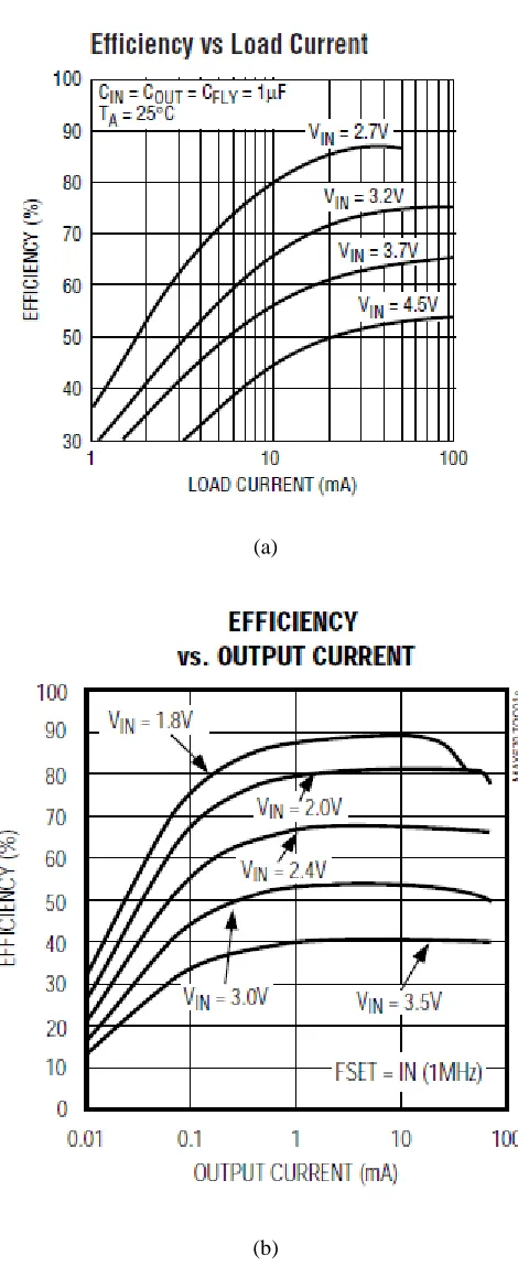
concept can be proved by analyzing the plots of the power conversion efficiency versus the load
current for two commercially available charge pumps shown in Fig. 1-1. It is quite noticeable that
the power conversion efficiency varies by 20-25% over the input voltage range in both the cases.
Linear Technology‟s LTC3200® charge pump is optimized to provide approximately 90% power
efficiency for the load current higher than 10 mA and it is noticeable in Fig. 1-1(a) [1]. Maxim‟s
MAX679® charge pump is designed to provide 80% to 90% power conversion efficiency for the
load current less than 10 mA. In modern CMOS processes, smaller device dimensions have
reduced the breakdown voltages and increased the oxide leakage current. This has restricted the
maximum voltage that can be handled on the chip. The switching power loss also dominates at
(a)
[image:15.612.190.425.67.642.2](b)
Figure 1-1. The plot of the power conversion efficiency versus the output load current for (a) LTC3200 IC (adapted
1.2 Research Objectives
The research work presented in this document focuses on the implementation, design and
mathematical analysis of the proposed charge pump architecture. The charge-pump-based DC-DC
converter is designed in the AMI 0.5 µm n-well CMOS process. The purpose of this work is to
explore an innovative approach to design a new charge pump architecture which can provide high
power efficiency and low output ripple noise.
Objectives of this research work include:
Develop a new charge pump architecture which has high power efficiency and low output
ripple voltage over a wide range of input voltage and load current.
Derive mathematical model for the proposed charge pump and use the model to predict the
performance of the proposed charge pump.
Design the proposed charge pump architecture in the AMI 0.5 µm n-well CMOS process
and simulate extensively to prove the concept.
1.3 Thesis Organization
This thesis is comprised of six chapters:
Chapter 2 reviews the inductor-based and charge-pump-based DC-DC converters. It also
compares the output noise, cost and portability between them. Also, the existing topologies of the
charge-pump-based converters are briefly summarized. The most commonly used regulation
schemes for the charge pump circuits are categorized and described to give better insight.
Chapter 3 proposes a new architecture for the charge pump and its design specifications for
battery-powered applications. Also, the transient operation of the proposed charge pump is
explained in detail along with the auxiliary circuits which are used to drive the charge pump
architecture. They are also beneficial in reducing unwanted power loss.
Chapter 4 provides a mathematical analysis of the charge pump architecture and derives the
output voltage equation and the transfer function for the same. Different power losses are taken
into consideration and mathematically derived to analyze their effect on power conversion
efficiency, output voltage regulation, and output ripple noise.
Chapter 5 discusses the simulation data over fifteen temperature and process corners.
Moreover, the effect of different input parameters on power conversion efficiency, output voltage
and output ripple voltage is analyzed to prove the concept.
Chapter 6 concludes the current research work and also elaborates on future enhancements
that can be made for the proposed charge pump circuit. It also discusses the buck converter
References
[1] LTC3200 Datasheet. http://cds.linear.com/docs/Datasheet/32005f.pdf
Overview of Existing DC-DC Converter 2
Circuits
2.1 DC-DC Converter Topologies
2.1.1. Inductor-based DC-DC converter
The conventional inductor-based DC-DC converter architecture has dominated moderate
and high-power integrated circuit applications. The typical configuration of an inductor-based
DC-DC converter architecture is shown in Fig. 2-1(a). It generally uses an inductor, a switch, a diode
and a load capacitor which is used to store the energy required to be delivered to the load [1].
Different topologies of DC-DC converter (i.e., buck converter, boost converter, inverting
converter) can be derived by placing the inductor in different ways in the circuit. One such
topology of an inductor-based boost converter is shown in Fig. 2-1(b).
(b)
[image:20.612.146.469.75.446.2](c)
Figure 2-1. (a) Inductor based DC-DC converter topology (b) Inductor based boost converter (adapted from [3]) and
(c) Timing diagram in the steady-state condition.
The inductor-based boost DC-DC converter, shown in Fig. 2-1(b), has two operating
phases which are the charge phase and discharge phase. During the charge phase, the switch is
open, the inductor current flows through the diode and charges the load capacitor. The load
capacitor is charged to the value equal to input voltage. When the switch closes during the
discharge phase, the diode is reverse-biased and the energy to the load is provided by the load
2-2.1.2. Switched-Capacitor (SC) based DC-DC converter
The switched-capacitor (SC)-based DC-DC converter is another widely-used alternative to
the inductor-based DC-DC converter in the medium power and low power handling applications.
As its name suggests, it uses switches and capacitors and is also called a charge pump. The
switches used in charge pump circuits fulfill the purpose of energy transfer from one stage to
another. Unlike the inductor-based DC-DC converter, charge pump architectures use capacitors for
energy transfer. These charge pump capacitors are known as flying or reservoir capacitors.
Depending upon the power handling requirement, the charge pump architectures are integrated
fully on-chip or partially on-chip since the sizes of capacitors are determined by the loading
requirement.
Like the inverter-based DC-DC converter, various voltage converter topologies (i.e.,
voltage doubler, tripler, step-down, negative converter) can result in SC-based architectures for
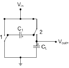
different orientations of the flying capacitors and switches. In Fig. 2-2, the architecture of a basic
[image:21.612.253.370.574.689.2]voltage doubler is depicted where Vin is the input supply voltage, Vout+ is the stepped-up output voltage, C1 is the flying capacitor and CL is the load capacitor. The charge transfer action of the voltage doubler shown in Fig. 2-2 is controlled by a dual-phase clock system.
The most commonly used charge pump circuit, known as the Dickson charge pump and its
timing diagram are shown in Fig. 2-3(a) and (b), respectively. Assuming the charge on the flying
capacitors C1, C2, and C3 is zero during the start-up condition, diode D1 is forward-biased when „clk‟ signal is low and „clk_bar‟ signal is high. The flying capacitor C1 charges to VDD voltage. When „clk‟ signal is high and „clk_bar‟ is low, the voltage at the anode terminal of D2 diode becomes 2*VDD and D2 is forward-biased. The charge stored in C1 capacitor is shared with C2 capacitor and the voltage across C2 capacitor becomes 0.5*VDD. When „clk_bar‟ signal goes high
in the next half cycle, diode D3 is forward biased and D2 is reverse-biased. The voltage across C2 is shared with C3 capacitor. The voltage across C3 capacitor after charge sharing is 0.25*VDD. In the next half cycle, „clk‟ signal goes high and diode D4 is forward-biased and D3 is reverse-biased. The output voltage VO with respect to ground is 1.25*VDD. Eventually, the output voltage VO becomes 2*VDD due to the sequential charge sharing action between the flying capacitors.
Figure 2-3. (a) Dickson charge pump architecture and (b) its timing diagram.
Selection between the architectures of a DC-DC converter is often debatable and is made
based on the power requirement of an application. The knowledge of the advantages and
disadvantages of both the architectures is also important for selection. The inductor-based DC-DC
converter architecture is less area-efficient compared to the charge-pump-based DC-DC converter.
The former uses a bulky inductor which is 5-10 times larger than the flying ceramic capacitors
used in the charge pump architecture. Even though the switching rate in modern systems has
increased and the size of inductor used in DC-DC converter has been reduced, the integration of an
inductor on the chip is still difficult compared to a capacitor. Moreover, the cost of an inductor is
also 5 to10 times higher than a flying capacitor used in the charge pump. If an analog designer
chooses to use a low quality inductor to reduce cost, the power conversion efficiency of an
The charge pump architecture is also an alternative to the inductor-based DC-DC converter
in high power density applications due to the use of off-chip capacitors in the former [1].
Generally, an inductor-based converter uses only one switch in a single stage of conversion. The
charge pump architecture has more than one switch depending upon its structure. Therefore, the
path from input to output is more resistive in the charge pump architectures. When the load current
requirement is higher, the conduction loss in the switches also increases. Due to power loss, the
output voltage degrades and power conversion efficiency also decreases. However, the research in
advanced process technology has made MOSFET switches available which exhibit less resistance
per unit chip area.
Another important metric for comparison between both types of DC-DC converters is the
output noise. There are a number of noise sources inherent in switch-mode power supplies. The
intrinsic noise generated by the DC-DC converter itself is dominant compared to noise generated
by external sources. The switching behaviors of the inductor-based voltage converter and charge
pump are very different. Their energy storage elements are also different. According to [3],
inductor-based and charge pump DC-DC converters generate noise at their switching frequency
and around its harmonics. Moreover, in an inductor-based DC-DC converter, additional output
noise is evident around its LC resonant frequency. The noise profiles of both types of voltage
Figure 2-4. Noise profiles of inductor-based and switched-capacitor-based DC-DC converters [2].
In modern DC-DC converters, the switching frequency can be quite high and in the range
varying from KHz to several MHz [4]. In inductor-based DC-DC converters, the inductor acts as
an antenna and emits electromagnetic signals at such high switching frequency. Other circuit parts
on the board may fail due to the Electro-Magnetic Interference, which is a big issue. Use of a
shielded inductor to avoid EMI only increases cost and area of the system. Thus, the use of
inductor-based DC-DC converters is avoided in the high switching frequency (RF) application.
Finally, the comparative analysis of the switched-capacitor DC-DC converter and the
inductor-based DC-DC converter shows that the former architecture is smaller in size and lower in
cost and generates less noise compared to the latter. The power conversion efficiency of the charge
(A) Topologies of Switched-Capacitor Based DC-DC Converter / Charge Pump
Charge pump circuits are often used as voltage doublers to fulfill the purpose of generating
higher bias voltages. As mentioned earlier, the flying capacitors are core elements used for voltage
conversion. The transfer of charge into and out of the flying capacitors is performed by MOSFET
switches at frequencies between KHz to tens of MHz, typically. Fig. 2-5 depicts four different
boost type charge pump architectures which are basic cascaded voltage doubler, ladder, Fibonacci
and multi-phase voltage doubler. Each of them has different orientation of the charge transfer
switches and capacitors and different charge transfer sequence. Their advantages and
disadvantages are explained in [5] and [6]. Each architecture has a voltage doubler as a basic cell
shown in Fig. 2-2 and the switches are turned on and off by two non-overlapping clocks having
50% duty cycle. The selection of charge pump topology is based on their respective characteristics.
(b)
(c)
(d)
Figure 2-5. (a) Dual phase cascaded voltage doubler (adapted from [6] and [7]) (b) Ladder charge pump architecture
(adapted from [5]) (c) Fibonacci charge pump architecture (adapted from [6]) and (d) Multiphase cascaded charge
(1) Dual Phase Voltage Doubler: The orientation of the transfer switches and capacitors in the
dual phase cascaded voltage doubler is shown in Fig. 2-5(a). Vin is the input DC power supply and
Vout+ is the stepped up output voltage. As its name suggests, the charge transfer action in the voltage doubler is controlled by two non-overlapping clocks. The ideal voltage gain for the dual
phase voltage doubler with N stages is A = 2*N [7]. In order to perform switching action, an N -stage dual phase voltage doubler involves 4*N charge transfer switches. As the charge pump architecture is designed fully on-chip or partially on-chip with external capacitors, the available
silicon area and the number of pins are critical constraints for an analog designer. For the dual
phase voltage doubler with N stages, the optimal performance can be achieved by using 2*N
capacitors with equal capacitance value [7].
(2) Ladder Charge Pump Architecture: The organization of the charge transfer switches, the
flying capacitors, and the load capacitor for the ladder charge pump architecture are shown in Fig.
2-5(b). Its switching action is also controlled by dual phase non-overlapping clocks. Ideally, the
ladder charge pump architecture with N stages has gain A = 2*N. An N-stage ladder charge pump requires 4*N charge transfer switches. To optimize the performance, 2*N capacitors with equal capacitance value are required for the ladder charge pump architecture with N stages.
(3) Fibonacci Charge Pump Architecture: During his study of the switched-capacitor voltage
multipliers, Makowski developed a new orientation of the switch-capacitor charge pump which has
voltage gain related to the Fibonacci numbers and is shown in Fig. 2-5(c) [7]. An N-stage Fibonacci charge pump architecture has 3*N+1 charge transfer switches and has gain equal to
voltage gain equal to 13). Thus, the voltage gain of an N-stage Fibonacci charge pump is higher or equal to that of an N-stage cascaded voltage doubler.
(4) Multiphase Charge Pump Architecture: A modern orientation of the multiphase charge
pump architecture is shown in Fig. 2-5(d). An N-stage multiphase charge pump architecture can provide 2N voltage gain with 4*N charge transfer switches and (2*N+1) capacitors of equal value. However, it requires 2*N clock signals which can be easily generated by a frequency division scheme [7].
(B) Unregulated Charge Pump and Regulated Charge Pump
In portable device applications like mobile phones, the system power supply voltage should
be stable and should not be affected by discharging the battery input voltage. In the unregulated
charge pump, the output voltage follows input voltage and is always a multiple of input. Such
behavior of the output voltage is not desirable in mobile phone devices. To maintain the output
voltage at a stable value, several regulation schemes have been implemented. The most commonly
used regulation methods involve current regulation, voltage regulation, and frequency regulation.
(1) Current Mode Regulation: A basic switched-capacitor charge pump, shown in Fig. 2-6
employs the current mode regulation scheme in which the current flowing through either single
MOS switch or multiple switches is controlled by a feedback voltage. Thus, the regulated MOS
switch acts as a current source [8]. If the output voltage goes below a certain voltage level, the
difference between the feedback/output voltage and the reference voltage is amplified by an error
through it. Due to the rise in the current flowing through the switch, the flying capacitor (Cfly) charges quickly and the output voltage returns to its stable level. The regulated MOS switch can be
either in the charging path or in the discharging path. The duty cycle of both the charging and
discharging phase should be set to 50% [8], [9].
Figure 2-6. Charge pump architecture with current mode regulation method (adapted from [8]).
(2) Voltage Mode Regulation: In this regulation method, the on-switch resistance of single or
multiple MOS switches is controlled by a feedback voltage as shown in Fig. 2-7. The regulation of
current is high or the input battery voltage goes low, the output voltage decreases and it is
compared against a stable reference voltage by an error amplifier. An error signal generated by the
error amplifier reduces the on-switch resistance and the voltage drop across the regulated switch
also goes down. If the battery voltage increases or the load current goes low, the output voltage of
the charge pump architecture increases. In this case, the error signal amplified by the error
amplifier increases the on-switch resistance and the voltage drop across the controlled MOS switch
also increases. The voltage mode regulation scheme can be employed in either the charging or
discharging path. Like the current mode regulation scheme, the duty cycle of non-overlapping
clock signals should be maintained at 50% and their frequency should be fixed.
(3) Frequency Regulation:
(A) Fixed Frequency Regulation (Pulse Width Modulation Technique):
In the fixed frequency regulation scheme, the duty cycle of the clock signal is modulated to
regulate the output voltage. The duty cycle modulation of the clock signal depends either on the
input voltage or on the load requirement [11]. The block diagram of pulse width modulation
control for charge pump architecture is shown in Fig. 2-8. If the input voltage increases or the load
current goes low, the output voltage of charge pump increases and it is fed back to an error
amplifier. The output of the amplifier is compared against a saw tooth waveform using a
comparator. For higher output voltage, the duty cycle of the clock signal becomes narrow and the
average power delivered to the load during each clock cycle goes down. In case of low output
voltage and high loading requirement, the output voltage decreases which causes an increase in the
duty cycle of the clock signal. Thus, the average energy delivered to the load during each clock
Figure 2-8. Schematic of buck charge pump with pulse width modulation technique (adapted from [11]).
(B) Variable Frequency Regulation:
B.1. Pulse Skip Regulation Method: In the pulse skip control scheme, the output voltage of the
charge pump is maintained at the desired value by omitting the unnecessary clock pulses [12]. The
regulated charge pump architecture with the pulse skip regulation method and the switching
signals are shown in Fig. 2-9. When the output voltage goes lower than the reference voltage, the
output load capacitance is charged continuously during each clock cycle. When the output voltage
is higher than the reference voltage, some clock pulses are skipped and the charge pump stops
providing energy to the load. During the pulse skipping, the average input current is quite low,
large frequency variation in the clock signal are disadvantages compared to the fixed frequency
regulation method.
(a)
(b)
B.2. Linear Skip Regulation Method: The linear skip control method is more complex than the
pulse skip regulation method and helps in enhancing the output ripple voltage performance of the
charge pump. The linear skip regulation scheme uses three phases of operation, which are wait
state, transfer phase, and charge phase [14]. When the load current is high, there is no wait state
and the current supplied to the output load is regulated by charge and transfer phases. When the
output voltage increases due to either high input voltage or low load current, the wait time
increases and the operation of the charge pump stops. During the wait state, the charge delivered to
the load is supplied by the load capacitor. Fig. 2-10 depicts the switching clock signals for the
linear skip regulation method employed in the switched-capacitor DC-DC converter.
.
Figure 2-10. Clock signals for different loading current requirement in linear skip regulation method (adapted from
References:
[1] M. D. Seeman, V. W. Ng, Le Hanh-Phuc, M. John, E. Alon, S. R. Sanders, “A Comparative Analysis of Switched-Capacitor and Inductor-Based DC-DC Conversion Technologies”, IEEE 12th Workshop on Control and Modeling for Power Electronics, pp. 1-7, June 2010.
[2] M. Renaud, Y. Gagnon, “Inductorless versus Inductor-Based Integration Switching Regulators: Bill of Material, Efficiency, Noise, and Reliability Comparisons”, Integration
Dolphin Inc.
[3] V. R. Tintu, M. George, “Tapped Inductor Technology Based DC-DC converter”,
International Conference on Signal Processing, Communication, Computing and
Networking Technologies, pp. 747 – 753, July 2011.
[4] F. Pan, T. Samaddar, “Charge Pump Circuit Design”, McGraw-Hill, New York, 1st
Edition.
[5] M. D. Seeman, S. R. Sanders, “Analysis and Optimization of Switched-Capacitor DC-DC
Converters”, IEEE COMPEL Workshop, pp. 216 – 224, July 2006.
[6] S. Krit, H. Qjidaa, I. E. Affar, Y. Khadija, Z. Messghati, Y. El-Ghzizal, “A Novel CMOS Charge-Pump Circuit with Current Mode Control 110 mA at 2.7 V for Telecommunication System”, IOP Science Journal of Semiconductor, Vol. 31, No. 4, pp.
045001-1 – 045001-5, April 2010.
[7] J. A. Starzyk, Y. Jan, F. Qiu, “A DC-DC Charge Pump Based on Voltage Doublers”,
[8] G. Thiele, E. Beyer, “Current Mode Charge Pump: Topology, Modeling and Control”,
IEEE 35th Annual Power Electronics Specialists Conference, PESC, Vol. 5, pp. 3812 –
3817, June 2004.
[9] S. Chaisotthee, J. Parnklang, “Low Swing CMOS Current Mode Charge Pump”,
International Conference on Control, Automation and Systems, pp. 1383 – 1386, Oct
2010.
[10] B. R. Gregoire, “A Compact Switched-Capacitor Regulated Charge Pump Power Supply”,
IEEE Journal Solid-State Circuit, Vol. 41, No. 8, pp. 1944 – 1953, Aug 2006.
[11] W. Lim, B. Choi, Y. Kang, “Control Design and Closed-Loop Analysis of a Switched-Capacitor DC-to-DC Converter”, IEEE 32nd Annual Power Electronics Specialists Conference, Vol. 3, pp. 1295 – 1300, June 2001.
[12] B. Kormann, “High-Efficiency, Regulated Charge Pumps for High Current
Applications”, Unitrode Design Seminar, 2001.
[13] Jae-Youl Lee, Sung-Eun Kim, Seong-Jun Song, Jin-Kyung Kim, Sunyong Kim, Hoi-Jun
Yoo, “A Regulated Charge Pump with Small Ripple Voltage and Fast Start-Up”, IEEE
Journal of Solid-State Circuits, Vol. 41, pp. 425-432, Feb 2006.
Architecture of the Proposed
3
High-Efficiency Charge Pump
3.1 Design Specifications
The worst-case performance goals of an unregulated switched-capacitor charge pump doubler
circuit are established in Table 3-1 which will be beneficial in investigating the proposed charge
pump architecture. These specifications are typical for display subsystems in modern portable
products such as cell phones and other mobile devices.
Parameter Specification Goal
Input Voltage Range 3 V – 6 V
Voltage Gain 2X
Load Current 2 mA – 45 mA
Power Conversion Efficiency 90%
Output Voltage 6 V – 12 V
Output Ripple Voltage 25 mV
Startup Time 2 ms
As mentioned earlier, modern integrated circuit systems manufacturers demand
high-efficiency power converters. Most of the discrete charge pump ICs available in the market offer
conversion efficiency ranging from 80% to 99%. High power conversion efficiency implies that
the ratio of the power delivered to the load to the input power provided to the system by the charge
pump architecture should be close to unity. Typical integrated charge pump architectures consume
several milliamperes under no-load condition. As a consequence, the charge pump architecture
exhibits low power conversion efficiency at light load current. The switched-capacitor charge
pump architecture presented in this thesis is designed to drive load currents ranging from 2 mA to
45 mA with efficiencies greater than 90%.
The proposed charge pump architecture, shown in Fig 3-1, is comprised of the charge
pump core and auxiliary circuits which include a non-overlapping clock generator, level shifters,
and well-switchers or well-managers. These auxiliary circuits are required to optimize the
performance of the charge pump core by minimizing the power losses (i.e., conduction loss,
reversion loss). The block diagram of the proposed charge pump architecture is depicted in Fig.
3-1.
3.2 Design of Auxiliary Circuits
3.2.1. Well-Switcher Circuit
The proposed step-up charge pump architecture is designed in the 0.5 µm n-well CMOS
process technology. During the startup condition, the internal node voltages of the charge pump
can swing from ground to any voltage less than . The body of the NMOS switch is connected
to ground voltage which is the lowest possible voltage in the circuit. The body of the PMOS switch
should be connected to the highest voltage in the circuit to avoid the forward biasing of the
source-body diode [1]. However, as mentioned earlier, the voltages at source and drain terminals of
PMOS switches can modulate between ground and . It is not viable to connect the body of
PMOS directly either to its source or to its drain. The auxiliary circuit shown in Fig. 3-2 helps in
Figure 3-2. Schematic of Well-Switcher Circuit
As depicted in Fig. 3-2, the body of charge transfer PMOS switch PM is connected to the
bodies of two auxiliary PMOS switches WP1 and WP2. The bodies of WP1 and WP2 are further
connected to their source terminals. The gate terminals of WP1 and WP2 are connected to the
source and drain terminals of the charge transfer switch PM, respectively. The source and drain
terminals of the PM switch are designated by P1 and P2, respectively. When the voltage at the P2
terminal of the PM switch is lower compared to the voltage at the P1 terminal, the WP1 switch
turns on and the WP2 switch turns off. The voltage of the P1 node of the PM switch is directly
applied to its body via the WP1 switch. A similar explanation can be given when the P1 voltage of
PM is lower than the voltage at P2. Thus, the body (n-well) connection of the charge transfer
switch PM is connected either to its source terminal or its drain terminal. Moreover, neither WP1
nor WP2 contribute to the reverse charge transfer or any leakage current. The well-switcher circuit
3.2.2. Clock Pair Generator Circuit
The choice of clocking frequency has a direct relationship with the size of flying
capacitors, the load current, and the output ripple voltage. Depending upon the output ripple
voltage and the load current specifications, the clocking frequency should be chosen such that it is
higher than the operating frequency of the loading circuit. In the proposed charge pump
architecture, the clocking frequency is 10 KHz +/- 20%. If many charge pumps are connected in
parallel and each of them is designed to deliver a fraction of the total load current, the sizes of
flying capacitors will decrease in each charge pump. In this case, the capacitors can be integrated
on-chip. However, an on-chip integrated capacitor has stray capacitance with respect to ground.
Eventually, it results in less power conversion efficiency. The model of the on-chip integrated
capacitance with the parasitic capacitances and its equivalent circuit model are depicted in Fig. 3-3
(a) and (b), respectively. According to one study, the maximum possible power conversion
efficiency of the charge pump was 50% with the on-chip poly-metal capacitor. On the other hand,
the same charge pump architecture exhibited 97% efficiency with external ceramic capacitors
under certain load conditions [2]. The block diagram of the clock pair generator circuit is shown in
(a)
(b)
Figure 3-3. (a) Graphical description of on-chip poly-poly capacitor along with parasitic capacitance. (b) The
Figure 3-4. Block Diagram of the Clocking Scheme for the Proposed Charge Pump Circuit.
(A) Non-overlapping Clock Generation
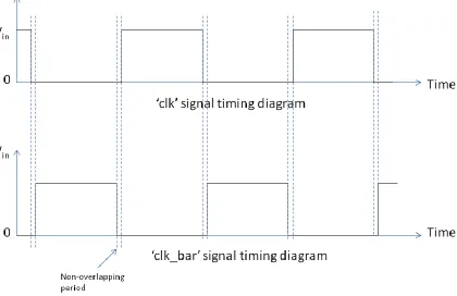
The proposed charge pump architecture uses non-overlapping clock phases to turn MOS
switches on and off, which prevents the short circuit condition between the high voltage node and
the low voltage node. The gate level schematic of the non-overlapping clock signal generator and
the clock signals are depicted in Fig. 3-5. The circuit shown in Fig. 3-5(a) operates in
„break-before-make‟ manner [3]. The phase difference between clock signals and is 180 and their
(b)
Figure 3-5. (a) Transistor Level Schematic of the Non-Overlapping Clock Signal Generator Circuit. (b) Input Clock
Signal (top) and Output Clock Signals clk_a (middle) and clk_b (bottom).
The non-overlapping period between both the clock signals can be varied by adding more
inverter delays. However, the large non-overlapping period keeps MOS switches in an open state
for a long time, which further causes leakage current glitches in input current. One such event of
Figure 3-6. The input current glitch during the non-overlapping period of and .
(B) Level Shifter
When the output voltage of the charge pump increases beyond the input voltage, , the
gate drive voltage of PMOS charge transfer switches should be equal to or higher than the output
voltage to turn them off properly. The complement is true for the NMOS switches where the gate
drive voltage should be equal to or higher than the output voltage to turn them on. Otherwise, the
charge transfer switches do not turn on or off properly and it results in short circuit power loss.
Figure 3-7. Conventional Level Shifter (adapted from [4]).
The level shifter used in the proposed charge pump architecture is shown in Fig. 3-8. The
conventional level shifter, shown in Fig. 3-7, offers large propagation delay [4]. The propagation
delay is caused due to pull-up and pull-down action of PMOS transistors and NMOS transistors,
respectively. The simultaneous action of pull-up and pull-down also gives rise to the switching
power which creates large current spikes on the supply rails. The simultaneous action of pull-up
and pull-down is mitigated in the level shifter used in the charge pump clocking scheme. The
quasi-inverters formed by PMOS transistors and stacked NMOS transistors help in pulling up or
pulling down the nodes A and B faster to their final values, which further reduces the dynamic
Figure 3-8. Contention Mitigated Level Shifter used in the Clocking Scheme of the Proposed Charge Pump.
The clock signal which is level shifted to the voltage level is shown in Fig. 3-9.
is the voltage fed back from the output of the charge pump and is the input voltage to the
charge pump. voltage is swept from 0 to to analyze the transient response of the level
Figure 3-9. The Transient Response of the Contention Mitigated Level Shifter When is swept from 0 to .
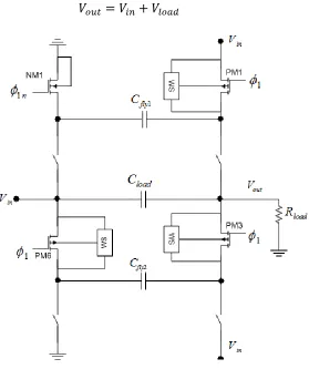
3.3 Operation of the Proposed Charge Pump Circuit
The transistor level design of the proposed charge pump DC-DC converter is shown in Fig
3-10. The design contains six PMOS and two NMOS switches for the charge transfer and three
capacitors for the charge storage. The switches are turned on and off by two non-overlapping
level-shifted clock signals, and , and their level-shifted complimentary signals, and ,
capacitor as shown in Fig 3-10. The body of PMOS switch is connected to the well-switcher
circuit. As the proposed charge pump architecture is designed in 0.5 µm CMOS n-well technology,
the well-switcher circuit ensures that the body of PMOS transistor is always connected to the
highest voltage during the active state of the charge pump. The body of NMOS switch is always
connected to the ground.
The architecture of the proposed charge pump is based on continuous current pumping
technique. In general, a charge pump is required to provide the load current, , all the time. The
input power supply should deliver enough charge during each clock cycle to fulfill the load current
requirement. A typical charge pump has two clocking phases: 1) Charge phase – during which the
charge is transferred to the load capacitor. 2) Discharge phase – during which the charge pump
stops pumping charge. The load current is provided by discharging the load capacitor during the
discharge phase. In the proposed architecture, the energy required to be delivered to the load is
continuously provided by either the top half or the bottom half of the charge pump to the load
capacitor. During a full cycle of the clock signal, there is no explicit discharge phase for the load
capacitor. However, the load capacitor discharges a small amount of charge to fulfill the load
Figure 3-11. The timing diagram of the proposed charge pump when it is operating in the steady state condition.
When goes low and becomes high logic during half cycle, their corresponding
complimentary signals and become high and low, respectively. The timing diagram is
shown in Fig. 3-11. The top half of the circuit is in charge phase and the bottom half of the circuit
is in discharge phase as shown in Fig 3-12. In top half of the charge pump architecture, PM1 and
NM1 switches are closed and PM1 switch allows the current to flow. The flying capacitor, ,
charges to the input voltage, , ideally. During this half cycle, the transistor switches PM2, PM4,
the circuit. The charge stored in the flying capacitor, , during half cycle is
transferred to the load capacitor, . In other words, is ideally charged to the input
voltage, , during half cycle. During half cycle, the voltage across the flying
capacitor, , appears across the load capacitor. The output voltage, , is given by:
[image:54.612.171.450.200.533.2](3-1)
Figure 3-12. The schematic of the proposed charge pump when goes low and becomes high.
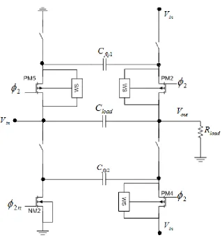
During the half cycle, goes high and goes low. The bottom half of the
circuit is in the charge phase and the top half of the circuit is in the discharge phase. The transistor
considered to be negligible, the flying capacitor, , is charged to the voltage . In the top
half of the charge pump architecture, and become parallel and the output voltage is
[image:55.612.151.470.158.504.2]given by (3-1).
Figure 3-13. The Schematic of the proposed charge pump when goes high and goes low.
References:
[1] L. Mensi, A. Richelli, L. Colalongo, Z. K. Vajna, "A Highly Efficient CMOS Charge Pump
[2] B. Kormann, " High-Efficiency, Regulated Charge Pumps for High Current
Applications ," Unitrode Design Seminar, pp. 1-14, 2001.
[3] M. Hoque, T. McNutt, J. Zhang, A. Mantooth, M. Mojarradi, "A High Voltage Dickson
Charge Pump in SOI CMOS," Proceedings of IEEE, Custom Integrated Circuit Conference, pp. 493-496, Sept 2003.
[4] C. Tran, H. Kawaguchi, T. Sakurai, "Low-power High-speed Level Shifter Design for
Analysis of the Proposed Low Noise
4
High-Efficiency Charge Pump
4.1 Mathematical
Model
of
the
Proposed
Charge
Pump
Architecture:
Ideally, the voltage conversion efficiency of any single-stage charge-pump-based DC-DC
converter is given by:
(4-1)
where K is the gain multiplier of the single-stage charge pump architecture and it depends upon the topology of charge pump (e.g., for voltage doubler cell, the value of K is 2). Equation (4-1) does not consider conduction losses, switching voltage loss and quiescent voltage loss. The voltage
conversion efficiency of the single-stage charge pump is 100% without those voltage losses.
Figure 4-1. Simplified DC model of charge pump (adapted from [1]).
A simplified DC model of DC-DC converter is shown in Fig 4-1. component causes
on-switch resistance of MOS on-switches, ESR of capacitors and parasitic resistances [1]. is the load
current. From the DC model, the output voltage of the DC-DC converter model can be given by:
(4-2)
The load current is required to be supplied all the time. The input power should supply enough
charge to fulfill the load current requirement during each half cycle. The charge required to be
delivered to the load during full clock cycle is given by:
(4-3)
During each half cycle, the charge supplied by the input power supply can be calculated by:
(4-4)
Thus, twice the load current flows through the flying capacitors, and during each half
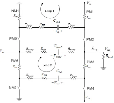
Figure 4-2. Simplified RC Model of the proposed charge pump when is low and is high.
Assume .
Assuming that the charge pump is operating in steady-state condition and not in start-up
state, the control signals and are low and high, respectively, during half clock cycle. A
simplified RC model of the proposed charge pump during half clock cycle is shown in Fig.
4-2. PMOS transistor PM1 and NMOS transistor NM1 are in the ON state in the top half of the
switches. As mentioned earlier, the loop current is twice the load current during half clock cycle.
Applying KVL in loop 1 as shown in Fig. 4-2, the voltage can be derived as follows.
(4-5)
(4-6)
where is the ON switch resistance of MOS charge transfer switch, is equivalent series
resistance of the external ceramic capacitor and accounts for the metal pin resistance and
the PCB route resistance. During the same phase, PMOS transistors PM3 and PM6 are also turned
on in the bottom half of the circuit. The flying capacitor, , is charged to voltage during
half cycle. The positive output voltage can be derived by using KVL for loop 2
shown in Fig. 4-2.
(4-7)
(4-8)
(4-9)
(4-10)
The value of across during half cycle is similar to that of during half
cycle. Therefore, the positive output voltage can be given by:
(4-11)
[image:61.612.119.502.338.689.2](4-12)
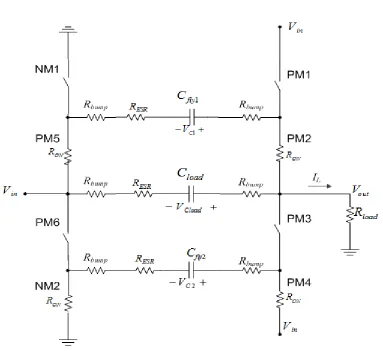
During half cycle, goes high and becomes low. PM1 and NM1 transistors
turn off first and then PM2 and PM5 transistors turn on to avoid the reversion loss. In the bottom
half of the circuit, PM4 and NM4 turn on and the flying capacitor, , is charged to . A
simplified model of the proposed charge pump is shown in Fig. 4-3 during half cycle.
The output voltage during half cycle can be derived in the same way as it is
[image:62.612.79.530.265.608.2]calculated for half cycle. The timing diagram the proposed charge pump is shown in Fig. 4-4.
Figure 4-4. The timing diagram of the proposed charge pump (a) , (b) , (c) , (d) , (e) , and (f)
continuously. There is no discharge phase during the operation of the charge pump. The
continuous current pumping technique is beneficial in achieving low ripple output voltage.
4.2 Design Considerations:
The definition of the power conversion efficiency given by (4-1) applies to an ideal DC-DC
converter system. In reality, there are several power losses in the DC-DC converter which play a
significant role in worsening the power efficiency. Taking power losses into account, the power
conversion efficiency, , is given by [1]:
(4-13)
where and are output power and input power, respectively. Input power also includes
total power loss due to the conduction loss, the charge redistribution loss, the reversion loss and
the switching loss. In order to achieve high efficiency, all power losses should be minimized [2].
The charge redistribution loss is due to charge transfer between capacitors. The conduction loss is
caused by non-ideal charge transfer due to resistive voltage drop across the transistor switches. The
reversion loss takes place due to back transfer of the charge from high voltage to low voltage. The
switching power loss is due to gate drives and parasitic capacitors and it is unavoidable to some
4.2.1 Conduction Power Loss:
The conduction power loss originates due to the ON resistance of MOSFET switches and
the equivalent series resistance (ESR) of the flying capacitors and the load capacitor. In the
proposed dual phase charge pump, MOSFET switches are used to connect and disconnect the
flying capacitors and the load capacitor with input supply and load [2]. According to (4-12), the
ON resistance of the switch plays a significant role in determining the output voltage. In
steady-state condition of the charge pump, these charge transfer switches operate in the linear region. The
ON switch resistance can be given by [4]:
(4-14)
In order to achieve high power efficiency, it is worth mentioning that low ON switch
resistance is mandatory. Furthermore, depends largely upon the aspect ratio of MOSFET
switches. By choosing proper aspect ratio for both NMOS and PMOS switches, the ON switch
resistances of both NMOS and PMOS switches can be made equal and low.
(4-15)
Moreover, also depends upon the threshold voltage of the device. To keep the ON switch
resistance low, threshold voltage should be kept low [4]. The threshold voltages of long channel
(4-16)
In order to keep threshold voltage low, the body voltage in NMOS should be held at the lowest
possible voltage which is the ground signal in the circuit [4]. Similarly, the body terminal in
PMOS should be connected to the highest possible voltage. The well-switcher circuit, discussed in
Chapter 3, helps in maintaining the body voltage of PMOS switches at the highest voltage in the
circuit. Thus, the threshold voltage of the PMOS charge transfer switch decreases and it further
reduces the ON switch resistance.
Moreover, the Equivalent Series Resistances (ESR) of the flying capacitors and the load
capacitor also contribute to the conduction power loss. The on-chip poly-poly capacitor or
metal-insulator-metal capacitor offers high ESR compared to the external ceramic capacitor. ESR
contributed by the external ceramic capacitor is in the range of several ohms (2 Ω - 4 Ω). The
conduction power loss can be calculated by:
(4-17)
(4-18)
4.2.2 Reversion Loss:
charge is transferred back to the lower voltage node. Reversion power loss can be optimized by
implementing the proper gate control scheme for the charge transfer switches [3].
In the proposed charge pump, the „break-before-make‟ clocking scheme is used to turn the
charge transfer switches on and off. This switching scheme ensures that the higher voltage node
should not be connected to the lower voltage node to avoid reverse transfer of the charge at any
time.
4.2.3 Charge Redistribution Loss:
The charge redistribution loss results from the non-ideal charge transfer between two
parallel capacitors. When two capacitors are connected in parallel, charge sharing between two
parallel capacitors takes place. This charge sharing event leaves its signature on the output of the
charge pump in the form of voltage ripples. Large ripple voltage is certainly an undesirable
quantity for systems like display driver, touch, microcontroller, etc.
When is high and is low, and are connected in parallel. The charge
is discharged through and and the output voltage changes from to during
half period as shown in Fig. 4-5. Applying the rule of charge conservation for the loop,
(4-19)
(4-20)
When is low and is high during half cycle, is placed on the top of and the
charge across is redistributed with the load capacitance. At the start of (i.e., )
half cycle, the output voltage increases from to . Applying the rule of charge conservation
for the corresponding loop,
(4-21)
Considering is equal to and solving (4-9) and (4-10) for and
(4-22)
(4-23)
(4-24)
Thus, the output ripple voltage is directly proportional to the load current and inversely
proportional to the clocking frequency, the flying capacitor and the load capacitor. By choosing the
proper capacitor and clocking frequency, the ripple voltage can be reduced to minimal value.
References
[1] Analogic Tech, “Application Note 113”, June, 2008.
http://www.eetasia.com/STATIC/PDF/200806/EEOL_2008JUN26_POW_ACC_AN_02.
[2] F. Su, W. Ki, C. Tsui, “High Efficiency Cross-Coupled Doubler with No Reversion
Loss”, IEEE International Symposium on Circuits and Systems, pp. 2761-2764, May 2006.
[3] J. Kim, Y. Jun, B. Kong, “CMOS Charge Pump With Transfer Blocking Technique for
No Reversion Loss and Relaxed Clock Timing Restriction”, IEEE Transactions on Circuits and Systems II, Vol. 56, No. 1, pp. 11-15, January 2009.
[4] D. Johns, K. Martin, “Analog Integrated Circuit Design”, John Wiley and Sons, 2nd
Simulation of the Proposed
5
Charge Pump
This chapter discusses the simulation results of the proposed architecture of the integrated
charge pump circuit. The key parameters (i.e., power conversion efficiency, output ripple voltage,
rise time) are simulated over 45 process, temperature and voltage corners which are listed in Table
5-1 below:
Corner Parameters Value
Temperature
-30
27
80
Process
tt typical NMOS and typical PMOS
ss slow NMOS and slow PMOS
ff fast NMOS and fast PMOS
sf slow NMOS and fast PMOS
fs fast NMOS and slow PMOS
[image:69.612.67.546.313.597.2]Voltage 3V, 5V and 7V
Table 5-1. List of process, temperature, and voltage corners used for simulating the proposed charge pump
The clock frequency is chosen to be 111 KHz to meet the design specifications. The clock
frequency for the simulation is calculated via (4-24). However, the effect of the clock frequency on
the different design specifications is investigated later in this section. Moreover, the effects of the
input range, the duty cycle, the clock frequency and the flying capacitor are also simulated and
discussed in the chapter over typical process corner and at the room temperature.
5.1 Transient Analysis Results
5.1.1 Start-up time
The start-up time of the proposed charge pump based DC-DC converter is simulated using
the transient analysis and is shown in Fig. 5-1 for the loaded and unloaded conditions, respectively.
It is depicted as the output voltage of the charge pump with respect to time. The rise time or the
start-up time can be defined as the time required for the output voltage to reach 95 % of its final
value. The start-up time of the charg
![Figure 2-1. (a) Inductor based DC-DC converter topology (b) Inductor based boost converter (adapted from [3]) and](https://thumb-us.123doks.com/thumbv2/123dok_us/110695.10398/20.612.146.469.75.446/figure-inductor-based-converter-topology-inductor-converter-adapted.webp)
![Figure 2-4. Noise profiles of inductor-based and switched-capacitor-based DC-DC converters [2]](https://thumb-us.123doks.com/thumbv2/123dok_us/110695.10398/25.612.92.519.84.299/figure-noise-profiles-inductor-based-switched-capacitor-converters.webp)