Journal of Physics D: Applied Physics
PAPER • OPEN ACCESS
Full-wave modelling of terahertz frequency plasmons in two-dimensional
electron systems
To cite this article: A Dawood et al 2019 J. Phys. D: Appl. Phys. 52 215101
1 © 2019 IOP Publishing Ltd Printed in the UK
1. Introduction
Two-dimensional electron systems (2DESs) are capable of supporting plasmons, which are slow electromagnetic waves caused by collective electron motion. In 2DESs formed in III-V semiconductor heterostructures, plasmon frequencies typically lie in the microwave to terahertz frequency ranges. Terahertz plasmons are particularly attractive as they could be exploited in a range of practical devices, and notably, emitters and detectors.
Ever since the pioneering works of Dyakonov and Shur [1, 2], one of the most commonly studied geometry for tera-hertz plasmon emitters and detectors is that based on the field-effect transistor (figure 1(a)). A 2DES is terminated by two
ohmic contacts, which allows application and detection of a dc voltage as well as the coupling-in and -out of terahertz waves [3–7]. Above the 2DES is a gate, which controls the electron density in the 2DES, and is frequently used for coupling into the free-space radiation. Variations of this basic structure have also been made, such double-grating-gate, meander-gate, and comb-gate devices [8–12].
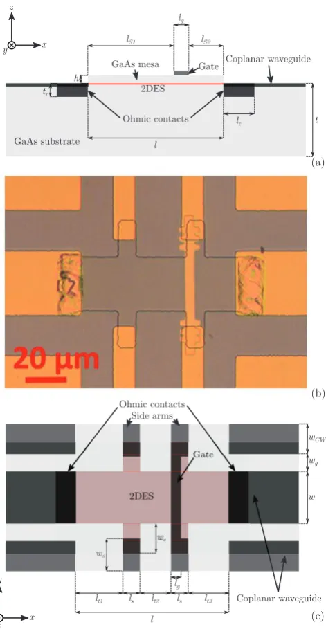
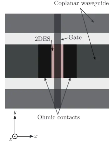
Theoretical studies of such devices have been made pre-dominantly with two-dimensional (2D) models [1, 14–24], in which the devices are assumed to be infinitely long in the y -direction (figure 1(a)). Three-dimensional (3D) models, however, may be needed to describe realistic devices, espe-cially when agreement with experiment is sought. As an example, figures 1(b) and (c) show, respectively, a micrograph and a sketch of the experimental device used by Wu et al [7,
13]. Several features that cannot be taken into account by a 2D model stand out. First, the width of the 2DES (25 µm
in the y -direction) is smaller than its length (73 µm in the
Journal of Physics D: Applied Physics
Full-wave modelling of terahertz frequency
plasmons in two-dimensional electron
systems
A Dawood1, J B Wu2, C D Wood3, L H Li3, E H Linfield3, A G Davies3, J E Cunningham3 and O Sydoruk1
1 Optical and Semiconductor Devices Group, Electrical Engineering Department, Imperial College London, SW7 2AZ, United Kingdom
2 Research Institute of Superconductor Electronics, School of Electronic Science and Engineering, Nanjing University, Nanjing 210093, People’s Republic of China
3 School of Electronic and Electrical Engineering, University of Leeds, Woodhouse Lane, Leeds, LS2 9JT, United Kingdom
E-mail: [email protected]
Received 11 December 2018, revised 5 February 2019 Accepted for publication 26 February 2019
Published 14 March 2019
Abstract
While models of terahertz frequency plasmons in 2D electron systems are usually developed by reducing the number of spatial dimensions, fully 3D models may be needed for the design and analysis of realistic structures. Using full-wave electromagnetic simulations, we have analysed the plasmons and magnetoplasmons observed in two recent experiments. Here, we demonstrate agreement between the theoretical and the experimental results, and discuss further device characteristics such as plasmon transmission, reflection, absorption, and field distributions. We then compare the 3D full-wave simulations with a 2D model. Finally, we discuss approaches for increasing signal transmission and reducing reflection, with direct relevance for improving future experiments.
Keywords: 2D electron systems, plasmon, terahertz, waveguides A Dawood et al
Full-wave modelling of terahertz frequency plasmons in two-dimensional electron systems
Printed in the UK
215101
JPAPBE
© 2019 IOP Publishing Ltd 52
J. Phys. D: Appl. Phys.
JPD
10.1088/1361-6463/ab0ab7
Paper
21
Journal of Physics D: Applied Physics IOP
Original content from this work may be used under the terms of the Creative Commons Attribution 3.0 licence. Any further distribution of this work must maintain attribution to the author(s) and the title of the work, journal citation and DOI.
2019
1361-6463
1361-6463/19/215101+10$33.00
x-direction). Second, the 2DES is connected at both ends to a coplanar waveguide. Third, the 2DES has a non-rectangular shape with four short stubs.
Full-wave numerical simulations are a natural choice for analysis of such structures. In this paper, we will:
1. compare a full-wave 3D electromagnetic model with the experiments by Wu et al [7] on plasmon- (section 3) and magneto-plasmon transmission (section 4);
2. analyse the experimental devices beyond the available experimental data (section 3);
3. compare the 3D model with a 2D model based on mode-matching (sections 3 and 4);
4. design and model a device geometry with improved char-acteristics (section 5).
2. Device structure and modelling considerations
Wu et al [7] formed a 2DES in a GaAs/AlGaAs heterostructure grown by molecular beam epitaxy. The depth of the 2DES was h = 75 nm. We have found that slight variations of the permit-tivity due to the detailed layer structure had little effect on the simulation results, and we assumed that the substrate material was GaAs, with a relative permittivity of 12.4, see figure 1. The dc electron density in the 2DES was n2D=6.5×1011 cm−2. The electron scattering time was determined from dc
conductivity measurements to be τ=33 ps. The device was formed by etching a rectangular mesa (see table 1 for dimen-sions). The mesa had four stubs connected to four metal lines, two of which were shorted to form a gate above the 2DES. We have found that including these features into simulations was needed for full agreement with experiments. Two ohmic contacts were formed at both ends of the mesa. A metallic gate was then deposited. An LT-GaAs layer grown on the same substrate allowed Wu et al to form two photoconductive switches, one at each side of the device (not shown in figure 1), which were used for excitation and detection of picosecond-duration current pulses. The pulses were both delivered to and extracted from the 2DES using two coplanar waveguides, the centre conductors of which were connected to the ohmic contacts (see figure 1). A negative voltage applied to the gate relative to an ohmic contact depleted the 2DES underneath the gate, and the relationship between the gate voltage and the electron density was found to be
Vg =
n
2D α1
1
γ −α2,
(1)
where Vg is in volts, n2D is in cm−2, α1=5.3813×1015 cm−2, α2=2.601, and γ=0.2295. In the experiments, the voltage typically varied between −0.4 and −2.4 V. Further details about the devices, experimental arrangement, and measure-ments can be found in [7, 13].
[image:3.595.55.291.61.521.2]When describing semiconductor plasmons theoretically, one has to choose how to model electron dynamics (both in Figure 1. (a) Schematic side view of a 2DES device used in the
experiments by Wu et al [7, 13]. The device geometry is inspired by the field-effect transistor. (b) Micrograph and (c) schematic top view of the device. The complex device geometry requires 3D modelling. Reproduced from [7]. CC BY 4.0.
Table 1. Dimensions used in simulations (see figure 1).
2DES length, l 73 µm
2DES width/width of centre conductor, w 73 µm
2DES depth/mesa height, h 75 nm Length of first ungated 2DES section, ls1 48.9 µm Length of second ungated 2DES section, ls2 19.7 µm Gate width/length of gated 2DES section, lg 4.4 µm
Stub width, ws 24 µm
Stub length, ls 11 µm
Width of 2DES side extension, we 14 µm
Separation between left contact and stub, lt1 16 µm Separation between stubs, lt2 21.9 µm Separation between right contact and stub, lt3 13.1 µm Coplanar waveguide gap, wg 20 µm
Width of waveguide ground plane, wcw 15 µm
Substrate thickness, t 50 µm Depth of ohmic contact, tc 1250 nm
[image:3.595.310.547.74.276.2]A Dawood et al
3 the 2DES and at the junctions) and the electromagnetic fields. This paper uses the standard model based on Euler’s hydro-dynamic equation of motion [1] that, in the absence of static magnetic fields, leads to an isotropic ac 2D Drude conduc-tivity of the form
σ2D= n2De 2
jωm∗1+ 1
jωτ
,
(2)
where e is the electron charge, m* is the effective electron mass and ω is the angular frequency. The paper also uses the
full system of Maxwell’s equations, which then dictate the boundary conditions.
We solved the equations using the rf module of the COMSOL Multiphysics® numerical package. The 2DES was modelled using a surface current density defined by (2). The ohmic contacts, the coplanar waveguides, and the gate were modelled as perfect conductors. The whole structure was enclosed in a bounding box with dimensions 223 µm ×100 µm ×60µm. Two sides of the bounding box
were used as excitation and detection ports, while the other sides were perfect electric conductors. The two outer (ground) conductors of the coplanar waveguides were connected to a perfectly conducting box along the length of the structure. This ensured that the even coplanar mode was excited, which was found to couple well to plasmons in the experiments (rather than the slot-line mode, which did not) [7]. The wave-guide sections to the both sides of the 2DES were 75 µm long.
3. Comparison with experiments: gate-modulation signals
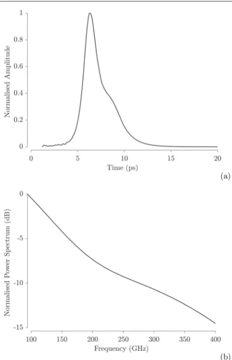
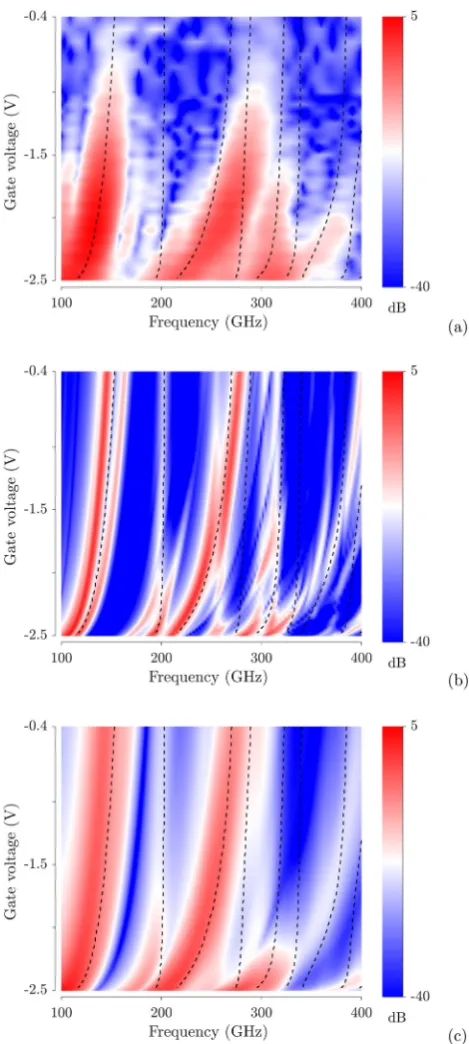
In the experiments, picosecond current pulses from a pho-toconductive switch were injected into one of the coplanar waveguides. Figure 2 shows the time-domain profile and the power spectrum of the input pulses. They then passed through the 2DES and coupled into the waveguide at the other side of the 2DES. This waveguide was connected to a second switch, where the transmitted pulses were detected. To increase the signal-to-noise ratio of the detected signals, a gate-modula-tion technique was used. The gate voltage was periodically modulated by a weak signal around a stationary value, which allowed Wu et al to employ lock-in detection. As a result, the detected signals were proportional to the absolute value of the derivative of the transmission coefficient with respect to the gate voltage. Figure 3(a) shows, as a colour plot, the exper imentally measured signals in the frequency range 100–400 GHz and for a range of gate voltages. The lines superimposed on the plot show the positions of the resonances calculated by a 2D mode-matching technique [24] as reported previously in [25].
In the simulations, we excite the even mode in the left coplanar waveguide at a single frequency, calculate its trans-mission to the waveguide on the opposite side, and then repeat the calculation for a range of frequencies and electron densities. The simulations are performed in the frequency domains with the same excitation power at every frequency.
[image:4.595.309.547.56.425.2]The experiments, however, excitation power effectively varied with frequency owing to the limited bandwidth of the pho-toconductive switch used for signal excitation (see figure 2). To allow direct comparison between the simulations and the experiments, we therefore scale the simulation results assuming an exponential decay of the excitation power with the frequency. We then calculate, using (1), the derivative of the transmission with the gate voltage.
Figure 3(b) shows the simulated gate-modulation signals for τ =33 ps, the value obtained from dc conductivity meas-urements. The simulated resonances are clearly narrower than the experimentally observed ones, indicating higher losses in the experiment than predicted from the dc value of the scattering time. Such reduction of the quality factors of the experimental terahertz resonances was observed in a number of other experiments that used different 2DES geometries and excitation and detection techniques. For example, Popov et al [26] found that the value of τ required to fit the absorption measurements in a grid-gated field-effect transistor was lower than the value predicted from the dc conductivity by roughly an order of magnitude. El Fatimy et al [27] reported that a plasmon resonance in a high-electron-mobility transistors measured experimentally had a quality factor of three, lower than the value of 13 expected from the measurements of the dc Figure 2. (a) Experimental time-domain input signals and (b) their frequency spectrum.
mobility. A number of explanations of the apparent reduction of the value of τ were proposed, such as different relaxation mechanisms involved at dc and the THz frequencies [28], bal-listic transport and viscosity [27], leakage of gated plasmons into ungated regions, and oblique modes [29]. No explanation appears so far to have gained wide acceptance. We note, how-ever, that our 3D model directly takes into account the inter-action of plasmons in the gated and ungated regions as well
as the plasmon field distribution both along and across the device, and so it is unlikely that plasmon leakage and oblique modes are responsible for the difference between figures 3(a) and (b). Following other authors, we have, therefore, decided to treat τ as a phenomenological parameter, and have repeated the calcul ations for a number of lower values of τ. We found the best agreement between the experiments and the simula-tions for τ =7 ps, as shown in figure 3(c).
Three strong features can be seen both in the theoretical and experimental plots. The first one starts at around 100 GHz for the lowest value of the gate voltage. The second starts at 200 GHz. The third lies around 300 GHz, and is strong only for low values of the gate voltage. The experimental features are shifted to the higher frequencies compared to the theor-etical ones. A possible reason for the shift is the approximate nature of (1) that was used to estimate the gate voltage from the theoretical values of the concentration. In the experiments, the gate voltage was measured directly. The maximum ampl-itudes of the experimental and modelled signals decrease with increasing frequency and with decreasing gate voltage. There are, however, differences in the relationships between the amplitudes of the peaks between the experiment and the simu-lations. It may be due to the complex shape of the excitation spectrum, which was not fully reproduced in the simulations.
4. Beyond experiment: transmission, reflection, absorption and field profiles
The use of the gate-modulation technique in the experiments was dictated by the need to increase the signal-to-noise ratio and eliminate direct cross-talk between the components on either side of the 2DES. In addition, the picosecond pulses used in the experiments delivered less power at higher fre-quencies, leading to weaker plasmon excitation.
On the other hand, numerical simulations are free from these constraints, allowing us to analyse the device across a wide parameter space. The colour plot in figure 4(a) shows the simulated transmission (S21) coefficient for τ=7 ps (as
[image:5.595.53.288.60.583.2]before, the dashed lines are the resonances calculated by the 2D model). More resonances can now be seen than in the gate-modulation plot of figure 3(c). This is because the resonances that depend weakly on the gated electron density are no longer suppressed, and the excitation amplitude is kept constant at all frequencies.
Figure 4(b) shows the transmission (S21, black line) at a
single value of the gate voltage, Vg=−2 V. It also shows the reflection (S11) and the absorption coefficients (blue and red
lines), the later calculated as 1− |S21|2− |S11|2. The reflec-tion and absorpreflec-tion of the signal dominate, and the trans-mitted signal does not exceed −25 dB. The transmission plot shows five resonances at 126, 192, 249, 300, and 358 GHz. To explain their nature, figure 5 shows the longitudinal (x-) comp-onent of the electric field, first, as contour plots in the plane of the 2DES (left column) and, second, across the middle of the 2DES (right column).
At the lowest-frequency resonance, only the gated sec-tion of the 2DES is excited strongly and evenly across the Figure 3. (a) Measured gate-modulation signals (data taken
A Dawood et al
5 width of the 2DES (y -direction). It has a single peak along the length (x-direction) of the gated section, which fits roughly a half of a plasmon wavelength. This is, therefore, the first lon-gitudinal gated-section resonance, and its position agrees well with the 2D calculation shown by dashed lines in figure 4(a).
At the next resonance, the longer (left-hand side) ungated section of the 2DES is excited in addition to the gated section. In the ungated section, the field maximum and minimum are reached at the opposite ends, and the field has a distorted half-wavelength pattern. The excitation amplitudes are higher at the 2DES edges, suggesting excitation of edge plasmons. The field in the gated portion of the 2DES is non-uniform across the width of the 2DES, showing both longitudinal and trans-verse plasmon excitation. The resonance position agrees well with the 2D calculation (see dashed line in figure 4(a)) which suggests that this resonance corresponds to the first-order lon-gitudinal resonance of the long section of the 2DES.
The third resonance, at 249 GHz, shows strong excitation of both the gated and the long ungated sections, each fitting around one plasmon wavelength. Even though the edges of the ungated section are also excited, it appears to be a predomi-nantly a longitudinal resonance that is a result of an interaction between the gated and the long ungated sections. The nature
of the resonance is confirmed, again, by the good agreement with the 2D model seen from figure 4(a).
The fields of the final two resonances are strongly non-uni-form across the width of the different 2DES sections. The gated 2DES shows both longitudinal and transverse plasmon excita-tion, with multiple field minima and maxima along the x- and y -directions. The long and short ungated 2DESs are excited strongly at the edges. As can be expected, the 2D calcul ations fail to predict the position of these two resonances.
5. Comparison with experiments: magnetoplasmons
Using the same device and technique, Wu et al detected mag-netoplasmon resonances in a magnetic field applied perpend-icular to the plane of the 2DES [13]. The colour plot in figure 6(a) shows the measured gate-modulation signals. The gate voltage was −2 V, and the magnetic field varied between 0 and 0.4 T. The dashed black lines show the position of 2D resonances found by the mode-matching technique. The red line is the cyclotron resonance.
In the presence of a static magnetic field B0 pointing in
the positive z-direction, the 2D Drude conductivity becomes anisotropic. The current density, J, can then be expressed as
J x Jy = env x envy = σ
xx σxy σyx σyy
Ex
Ey
(3)
where
σxx=σyy =e 2n
2D
m∗
jω+τ1
jω+1τ2+ω2c
(4)
σxy =−σyx =e 2n
2D
m∗
ωc
jω+τ12+ω2c
(5)
[image:6.595.52.289.60.405.2] [image:6.595.355.553.362.483.2]and ωc=eB0/m∗ is the cyclotron frequency.
Figure 6(b) shows the gate-modulation signals simulated using (3)–(5). The qualitative agreement with the experiment is good for the features lying below 300 GHz. As before, the difference in the relative strength of the measured and sim-ulated resonances can be attributed to the spectrum of the excitation pulses. Some of the resonances modelled above 300 GHz do not show in the measurements, possibly because the excitation signals were weak. To the right of the cyclotron line, the simulations predict a strong signal but only a faint feature can be seen in the measurements.
While figures 6(a) and (b) show the gate-modulation sig-nals, figure 7 shows the simulated true transmission coeffi-cient. The maximum transmission does not exceed −25 dB for all values of the magnetic field. The behaviour of the lowest resonance with the magnetic field agrees well with the prediction of the 2D model. The next two resonances agree well with the 2D model at low magnetic field. They do not follow, however, the parabolic behaviour of the 2D curves, and it leads to a discrepancy between the 3D simulation and the 2D model at higher fields. As can be expected from the Figure 4. (a) Modelled true transmission for a range of gate
voltages and (b) transmission, reflection and absorption at a gate voltage of −2 V in the device. The absorption and reflection dominate, and the transmission does not exceed −25 dB.
A Dawood et al
[image:8.595.337.512.64.292.2] [image:8.595.51.290.64.394.2]7 results for zero magnetic field discussed above, the full-wave 3D simulations and the 2D model disagree in their predic-tions of the resonance posipredic-tions. We attribute this disagree-ment to the excitation of edge plasmons and of transverse plasmons (with non-trivial component of the wavenumber in Figure 6. (a) Measured (data taken from [13]) and (b) simulated gate-modulation signals for magneto-plasmons. Theory and experiment agree for features between 100 and 300 GHz.
[image:8.595.311.548.354.674.2]Figure 7. Simulated true transmission for the same structure as in figure 6. The dashed lines show positions of the resonances predicted by the 2D modal technique.
Figure 8. Top view of the device with improved characteristics. A shorter overall length reduces absorption, and connecting the gate and the ground planes of the coplanar waveguides provides better coupling between the 2DES and the waveguides.
Figure 9. Simulated transmission (a) as a function of gate voltages, and (b) the transmission, reflection, and absorption characteristics at a gate voltage of −2 V for the device of figure 8. At 164 GHz, the transmission is around −3 dB, and the reflection is below −15 dB.
[image:8.595.54.290.441.618.2]the y -direction), both of which are not taken into account by the 2D model.
6. Improving device performance
The simulated transmission for the experimental device did not exceed 25 dB, as shown in figures 4 and 7. Such a low value is due to two factors: high plasmon absorption in the 2DES, and high signal reflection between the 2DES and the coplanar waveguides (figure 4(b)). The plasmon loss could be reduced by shortening the length of the 2DES. The high reflec-tion can be attributed to the dissimilar field distribureflec-tions in the 2DES and the coplanar waveguides. The even mode supported by the coplanar waveguide is a quasi-TEM mode whose field is concentrated in the gaps between the centre and the ground conductors [30]. On the other hand, plasmons are TM modes whose field is concentrated around the 2DES. Rearranging the waveguide electrodes to create high electric field along the 2DES is, therefore, likely to improve the coupling. It can be done by connecting the gate and the ground electrodes via a capacitor (which will decouple the gate and the ground at dc allowing voltages to be applied to the gate).
A possible device is shown schematically in figure 8. The length of the gated section here is 4 µm, and the ungated
sections have been both reduced to 2 µm. The device width
remains 30 µm. Figure 9(a) shows the simulated transmission
for a range of voltages, and figure 9(b) shows the transmis-sion, reflection and absorption for the gate voltage of −2 V. Improvements can be seen upon comparing figure 9 for the new device to figure 4 for the original experimental device. The maximum transmission has increased by over 20 dB for the peak at 165 GHz. The reflection has also decreased by a similar amount. The observed three resonances correspond to the excitation of the longitudinal gated plasmons, as can be seen from the field distributions shown in figure 10 for Vg=−2 V at 164, 272 and 393 GHz. The peak frequencies are close to the three lowest resonant frequencies of longitu-dinal gated plasmons (144, 279, and 407 GHz) assuming an integer number of plasmon wavelengths in the gated section.
7. Conclusions
[image:9.595.121.485.58.436.2]A Dawood et al
9 gate-modulation, both for plasmons and magnetoplasmons. We used this model to analyse device characteristics that could not be directly measured in experiments, such as the true transmission, reflection, and absorption, as well as to study the field distributions at the transmission maxima. We also compared the predictions of the fully 3D model with a 2D model based on modal expansions. While the frequen-cies of some plasmon resonances could be explained equally well by both approaches, the full-wave simulations showed additional resonances that we attribute to plasmon excita-tion across and at the edges of the device. Our calculaexcita-tions predict the transmission in the experimental devices to be below −25 dB, in part due to the high plasmon absorption, and in part due to high reflection. By reducing the length of the ungated sections and modifying the coupling geom-etry between the 2DES and the coplanar waveguides, we presented a device in which the maximum transmission increased by 20 dB.
Acknowledgments
The authors are grateful to Dr S Zonetti and Mr S Siaber for helpful discussions. C D W, E H L, L L, A G D, J E C, and OS acknowledge the financial support by the EPSRC (Grant Nos. EP/R004994/1, EP/R00501X, and EP/P021859/1). E H L acknowledges support of the Royal Society and Wolfson Foundation. Data underlying this article can be accessed at
https://doi.org/10.5281/zenodo.2586740, and used under the Creative Commons Attribution licence.
ORCID iDs
O Sydoruk https://orcid.org/0000-0003-3855-1003
References
[1] Dyakonov M and Shur M 1993 Shallow water analogy for a ballistic field-effect transistor: new mechanism of plasma wave generation by a dc current Phys. Rev. Lett.71 2465–8 [2] Dyakonov M and Shur M 1996 Detection, mixing, and
frequency multiplication of terahertz radiation by two-dimensional electronic fluid IEEE Trans. Electron. Dev. 43 380–7
[3] Knap W, Lusakowski J, Parenty T, Bollaert S, Cappy A, Popov V Ṽ and Shur M S 2004 Terahertz emission by plasma waves in 60 nm gate high electron mobility transistors Appl. Phys. Lett.84 2331
[4] Ryzhii V, Khmyrova I, Ryzhii M, Satou A, Otsuji T, Mitin V and Shur M S 2008 Plasma waves in two-dimensional electron systems and their applications Physics and Modelling of Tera- and Nano Devices ed M Ryzhii and V Ryzhii (Singapore: World Scientific) pp 77–94 [5] Dyer G C, Vinh N Q, Allen S J, Aizin G R, Mikalopas J,
Reno J L and Shaner E A 2010 A terahertz plasmon cavity detector Appl. Phys. Lett.97 193507
[6] Dyer G C, Aizin G R, Allen S J, Grine A D, Bethke D, Reno J L and Shaner E A 2013 Induced transparency by coupling of tamm and defect states in tunable terahertz plasmonic crystals Nat. Photon.7 925–30
[7] Wu J B et al 2015 Excitation, detection, and electrostatic manipulation of terahertz-frequency range plasmons in a two-dimensional electron system Sci. Rep.515420 [8] Otsuji T, Hanabe M, Nishimura T and Sano E 2006 A
grating-bicoupled plasma-wave photomixer with resonant-cavity enhanced structure Opt. Express14 4815–25
[9] Otsuji T, Meziani Y M, Hanabe M, Ishibashi T, Uno T and Sano E 2006 Grating-bicoupled plasmon-resonant terahertz emitter fabricated with GaAs-based heterostructure material systems Appl. Phys. Lett.89263502
[10] Otsuji T, Meziani Y M, Nishimura T, Suemitsu T, Knap W, Sano E, Asano T and Popov V V 2008 Emission of terahertz radiation from dual grating gate plasmon-resonant emitters fabricated with InGaP/InGaAs/GaAs material systems J. Phys.: Condens. Matter20 384206 [11] Białek M, Czapkiewicz M, Wróbel J, Umansky V and
Łusakowski J 2014 Plasmon dispersions in high electron mobility terahertz detectors Appl. Phys. Lett.104 263514 [12] Białek M, Witowski A M, Orlita M, Potemski M,
Czapkiewicz M, Wróbel J, Umansky V, Grynberg M and
Łusakowski J 2014 Plasmonic terahertz detectors based on a high-electron mobility GaAs/AlGaAs heterostructure
J. Appl. Phys.115 214503
[13] Wu J B, Sydoruk O, Mayorov A S, Wood C D, Mistry D, Li L, Linfield E H, Davies A G and Cunningham J E 2016 Time-domain measurement of terahertz frequency magnetoplasmon resonances in a two-dimensional electron system by the direct injection of picosecond pulsed currents
Appl. Phys. Lett.108 091109
[14] Mikhailov S A 1998 Plasma instability and amplification of electromagnetic waves in low-dimensional electron systems
Phys. Rev. B 58 1517–32
[15] Crowne F J 2000 Dyakonov–Shur plasma excitations in the channel of a real high-electron mobility transistor J. Appl. Phys.87 8056–63
[16] Ryzhii V, Satou A and Shur M S 2003 Admittance of a slot diode with a two-dimensional electron channel J. Appl. Phys.93 10041–5
[17] Satou A, Ryzhii V and Chaplik A 2005 Plasma oscillations in two-dimensional electron channel with nonideally conducting side contacts J. Appl. Phys.98 034502 [18] Popov V V, Polischuk O V and Shur M S 2005 Resonant
excitation of plasma oscillations in a partially gated two-dimensional electron layer J. Appl. Phys.98033510 [19] Popov V V, Tsymbalov G M and Shur M S 2008 Plasma
wave instability and amplification of terahertz radiation in field-effect-transistor arrays J. Phys.: Condens. Matter 20 384208
[20] Aizin G R and Dyer G C 2012 Transmission line theory of collective plasma excitations in periodic two-dimensional electron systems: finite plasmonic crystals and tamm states
Phys. Rev. B 86 235316
[21] Sydoruk O, Syms R R A and Solymar L 2012 Distributed gain in plasmonic reflectors and its use for terahertz generation
Opt. Express20 19618–27
[22] Sydoruk O, Syms R R A and Solymar L 2012 Amplifying mirrors for terahertz plasmons J. Appl. Phys.
112 104512
[23] Sydoruk O 2013 Drifting plasmons in open two-dimensional channels: modal analysis J. Phys. D: Appl. Phys.
[24] Sydoruk O, Choonee K and Dyer G 2015 Transmission and reflection of terahertz plasmons in two-dimensional plasmonic devices IEEE Trans. Terahertz Sci. Technol. 5 486–96
[25] Sydoruk O, Wu J B, Mayorov A, Wood C D, Mistry D K and Cunningham J E 2015 Terahertz plasmons in coupled two-dimensional semiconductor resonators Phys. Rev. B 92195304 [26] Popov V V, Polischuk O V, Teperik T V, Peralta X G,
Allen S J, Horing N J M and Wanke M C 2003 Absorption of terahertz radiation by plasmon modes in a grid-gated double-quantum-well field-effect transistor J. Appl. Phys. 94 3556–62
[27] El Fatimy A et al 2006 Resonant and voltage-tunable terahertz detection in in Ga As/ in P nanometer transistors Appl. Phys. Lett.89 131926
[28] Tyson R E, Stuart R J, Hughes H P, Frost J E F, Ritchie D A, Jones G A C and Shearwood C 1993 Non-linear doppler shift of the plasmon resonance in a grating-coupled drifting 2DEG Int. J. Infrared Millim.14 1237–49
[29] Shchepetov A et al 2008 Oblique modes effect on terahertz plasma wave resonant detection in in Ga As/ in Al As multichannel transistors Appl. Phys. Lett.92 242105 [30] Simons R N 2001 Coplanar Waveguide Circuits, Components,