Int. J. Electrochem. Sci., 12 (2017) 8651 – 8662, doi: 10.20964/2017.09.42
International Journal of
ELECTROCHEMICAL
SCIENCE
www.electrochemsci.org
Short Communication
Characterization of the Electrical Properties of Silicon
Nanowire using the Dielectrophoretic Assembling Platform
Yen-Heng Lin1,2,3,*, Jing-Chao Wong2, Yong-Sheng Peng1
1
Department of Electronic Engineering, Chang Gung University, Taoyuan 333, Taiwan
2
Graduate Institute of Medical Mechatronics, Chang Gung University, Taoyuan 333, Taiwan
3
Department of Otolaryngology-Head & Neck Surgery, Chang Gung Memorial Hospital, Taoyuan 333, Taiwan
*
E-mail: yenheng@mail.cgu.edu.tw
Received: 11 April 2017 / Accepted: 7 July 2017 / Published: 13 August 2017
In this study, the electrical properties of silicon nanowire were measured with a dielectrophoresis alignment platform. A pair of nickel electrodes spaced 10 µm apart was fabricated on a quartz substrate using a lithography process. Then, silicon (Si) nanowires in the solution were attracted to the electrodes near them with an aid of dielectrophoretic force. As a result, Si nanowires that were longer than 10 µm in length bridged the gap between the electrodes, forming a pair of Si nanowire sensors. Under an AC voltage with an amplitude of 10 Vpp and a frequency of 100 kHz, approximately 20 Si nanowires can bridge the gap between the electrodes within approximately 10 s. After the solution evaporated, the Si nanowires were fixed by clamping them onto the upper and lower nickel electrodes using a second lithography process and a metal deposition process. Characterizations based on the current–voltage curve showed that this fixing process can reduce the contact resistance between the nickel and Si nanowires and allow an ohmic contact to form between them. Consequently, the properties of the devices became more stable, which verified the possibility of using the assembled Si nanowire sensors as biosensors.
Keywords: silicon nanowire, nanowire sensor, dielectrophoresis, microfabrication
1. INTRODUCTION
researchers have been continuously studying one-dimensional (1D) nanomaterials. At the same time, 1D nanostructures-nanowires have also been widely applied and discussed. Because of their extremely small feature sizes and high surface-to-volume ratios, in a number of studies, nanowires have been used in electronic devices to improve their physical or electrical properties. For example, nanowires have been used in nanoscale photoelectric element solar cells [2-3], light-emitting diodes [4], and fuel cells [5]. In addition, nanowires are suitable for nanoscale biosensors. Because these nanomaterials, which are approximately 10–100 nm in size, have comparable sizes to biomolecules (e.g., proteins, deoxyribonucleic acids, viruses, and bacteria) and relatively large surface reaction areas, nanoscale biosensors are more sensitive in sensing biomolecules; furthermore, they are also advantageous in that they can perform label-free sensing in real time [6-9].
Generally speaking, there are two types of processes used to fabricate nanowire devices, top-down and bottom-up [10-12]. In the top-top-down process, the nanowire material is first deposited on a substrate. Then, the nanowire pattern on the photomask is transferred onto the substrate using an E-beam photolithography process. Finally, the nanowire structure is fabricated by means of reactive ion etching. In the bottom-up process, nanowires are first synthesized using chemical vapor deposition (CVD). Then, the synthesized nanowires are arranged on the metal electrodes on a substrate. The top-down fabrication process can be used to produce nanowires in large numbers with semiconductor processing techniques. However, the top-down fabrication process relies on high-resolution photolithography, the realization of which requires costly equipment. In addition, the minimum width of nanowires prepared using the top-down fabrication process is also limited by the photolithography equipment. In comparison, the bottom-up technique is relatively flexible in regard to the nanowire materials and sizes. In addition, the bottom-up technique also only requires relatively low-cost equipment. Therefore, a convenient, effective method for assembling nanowires on electrodes is the key to whether the bottom-up method can be extensively used.
For bottom-up assembly of nanowires, several methods for arranging nanowires on electrodes or substrates have been reported, for example, the lubricant-assisted contact printing method [13,14]. The use of a lubricant can prevent collision and friction between nanowires during the contact printing process and arrange nanowires in a uniform direction in large areas. However, the shortcoming of the lubricant-assisted contact printing method lies in that it cannot effectively control the number of nanowires being arranged. In addition, in 2009, Sharma et al. arranged nanowires using an evaporation-induced alignment method [15,16]. This method can simply place nanowires in an orderly arrangement using a capillary force and is suitable for arranging nanowires in large areas. However, similar to the lubricant-assisted contact printing method, the disadvantage of the evaporation-induced alignment method also lies in that it cannot easily control the number of nanowires being arranged. The method involving the use of a dielectrophoretic (DEP) force to arrange nanowires or nanorods is widely used, which is a non-contact method. Nanowires or nanorods are polarized in an electric field, and consequently, they are arranged in a direction consistent with the direction of the electric field. This method can be used to assemble nanorod structures [17-19] with superlattices.
nanowires, roughly control the number of nanowires, and requires simple equipment [20, 21]. After the Si nanowires were arranged on the metal electrodes, a second photolithography process was used to deposit a second layer of metal on the Si nanowires to form a metal/nanowire/metal sandwich structure [22] and then the electrical characterization was measured. This structure was created to clamp the Si nanowires between the two layers of metals. This method is different from the method that uses a high-energy laser beam to melt the two ends of the nanowires and welds the nanowires to the metal electrodes using their melted ends because a high-energy laser beam requires a precision operating platform [23] and may damage the sensor structure.
2. MATERIALS AND METHODS
2.1. Principle of attraction of nanowires by a DEP force
[image:3.596.58.533.380.586.2]Dielectrophoresis refers to a phenomenon in which a dielectric particle is polarized in a non-uniform electric field; the particle thus develops an induced electric dipole, which, under an external electric field, generates a force that attracts or repels the electric field. This force is referred to as a DEP force (Figure 1).
Figure 1. When a silicon nanowire was exposed to an AC electric field, a dipole moment was induced, and the positive and negative charges were separated to the two ends of the nanowire. The interaction between the dipole moment and the applied AC electric field attracted the nanowire toward the metal electrodes.
In this study, a solution containing nanowires was transferred dropwise onto the metal electrodes. When an AC signal was applied on the left and right metal electrodes, the DEP force was induced, the magnitude of which can be expressed as follows [24]:
where r represents the radius of the nanowire; l represents the length of the nanowire; εm represents the
dielectric constant of the solution; E2 represents the gradient of the square of the electric field; and Re[fcm] represents the real part of the Clausius–Mossotti (CM) factor. The CM factor can be expressed
as follows:
(2)
where represents the dielectric constant of the nanowire and represents the dielectric constant of the surrounding solution. The dielectric constant can be expressed as , where σ and ω represent the conductivity and the angular frequency of the electric field, respectively. Based on the aforementioned equations, the magnitude of the DEP force is affected by the length and radius of the nanowire, the intensity of the external electric field, and the CM factor. Whether the CM factor has a positive or negative value is related to the complex dielectric permittivity of the nanowire and the solution. When the dielectric constant of the surrounding solution remains unchanged, we can alter the magnitude and sign (attractive or repulsive) of the DEP force by controlling the frequency of the external electric field. In this study, a positive DEP force was required to attract the nanowires to the two ends of the electrodes.
2.2. Arrangement of the silicon nanowire on the electrodes
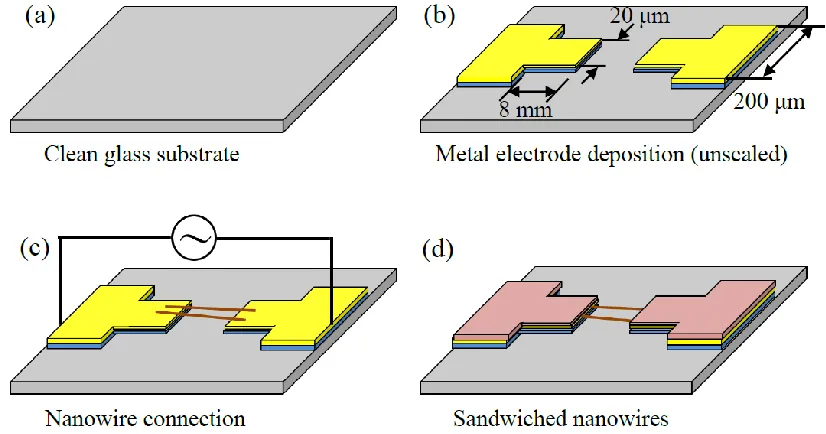
Quartz glass (Rocoes Electro-optics Co., Ltd., Taiwan) was used as the substrate. First, the substrate was cleaned by immersing it in a piranha solution (sulfuric acid/hydrogen peroxide, 3/1 (v/v)) at 80 ˚C for 30 min (Figure 2a).
[image:4.596.90.503.465.682.2]
Then, the metal electrodes to be bridged by nanowires were fabricated using the lift-off technique. The pattern of the metal electrodes was produced using a photolithography process with an S1818 positive photoresist (Dow Electronic Materials, USA). Subsequently, a thermal evaporator (TH400, LJUHV Co. Ltd., Taiwan) was used to first deposit a 10-nm thick chromium (Cr) layer as the adhesive layer and then deposit a 20-nm thick nickel (Ni) layer as the electrodes in 5×10⁻⁶ Torr vacuum chamber. Finally, acetone was applied to remove the photoresist and excess metals (Figure 2b). Afterwards, a Si nanowire solution was dropped onto the metal electrodes on the substrate. In addition, an AC voltage with a frequency of 100 kHz and an amplitude of 10 Vpp was applied on the two ends of the electrodes to generate an attractive DEP force, by which the nanowires were attracted onto the electrodes (Figure 2c). After the solution was evaporated, a second layer of metal was used to fix the nanowires. Because the nanowires were only placed on the electrodes physically, the substrate was cleaned without a solution to prevent the nanowires from being washed away by the solution via surface tension. Instead, the substrate was subjected to an oxygen plasma cleaning treatment for 10 min using a PDC-001 cleaner (Harrick Plasma, USA) operated at 30 W. After the substrate was cleaned, a second photolithography process was performed using a mask aligner (ABM Inc., USA) to expose the areas of the two ends of each nanowire that were in contact with the metals. Subsequently, the substrate was immersed in a buffered oxide etch (BOE, hydrofluoric acid/ammonium fluoride 1/6, J.T. Baker, USA) for 5 s to etch the native oxide on the nanowires. Then, 100-nm thick Ni was deposited on the nanowires using the thermal evaporator. This sandwich structure was used to clamp and fix the nanowires between the two layers of metals (Figure 2d) to reduce the contact resistance.
2.3. Si nanowire solution preparation and DEP platform setup
[image:5.596.67.535.468.663.2]
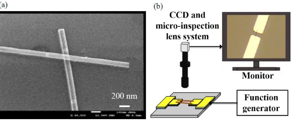
The Si nanowires were synthesized through CVD with argon as the carrying gas, silane as the source of Si, and diborane as the source of the dopant boron. The synthesis process of Si nanowires follows the vapor-liquid-solid growth mechanism [25]. This process requires the addition of gold nanoparticles as the catalyst to induce the reactants to undergo adsorption, dissolution and oversaturation and, eventually, the formation of nanowires. The detailed processes of Si nanowire synthesis were previously described [26, 27]. Because Si atoms are melted on the gold nanoparticles to form alloy nanoparticles, the gold nanoparticle size will affect the Si nanowire diameter. In the present study, gold nanoparticles (Top Nano Technology, Taiwan) with a diameter of 100 nm were used, and the prepared Si nanowires had a diameter of approximately 100 nm (Figure 3a). In addition, the synthesized Si nanowires were approximate 15-20 μm in length. The larger the nanowire, the greater the DEP force that is exerted on the nanowire wire [28].
The wafer (Summit-tech, Taiwan) with completely formed Si nanowires was placed in a microcentrifuge tube. Then, isopropyl alcohol (IPA, Sigma-Aldrich, Taiwan) was added to the microcentrifuge tube. After the microcentrifuge tube was subjected to gentle oscillation in an ultrasonic oscillator for 5–10 s, the nanowires were shaken off the wafer and dispersed in the IPA solution. Whether the nanowires were dispersed in the IPA solution can be determined based on the color of the solution. Figure 3b shows the setup of the nanowire sensor assembly platform. A signal generator (33210A, Agilent, USA) connected to the metal electrodes on the quartz substrate was used to provide an AC electric field. The assembly process was observed in real time using a micro-inspection lens system (Zoom 125C, OPTEM, USA) and a charge-coupled device (CCD, STC-620PMT, SENTECH, Japan). A semiconductor parameter analyzer (4200-SCS, Keithley, USA) was used to determine the current–voltage (I–V) characteristic curves of the assembled nanowire sensors.
3. RESULTS AND DISCUSSION
3.1. Metal electrode fabricationand the advantage of using DEP for assembly
Nine pairs of Ni electrodes were arranged in a 4-cm2 area. This design allowed for simultaneous observations in the same field of view of the bridged gap (Figure 4a). The front ends of each pair of electrodes were 20 µm in width and 8 mm in length, and the wires connected to the back ends of the electrodes were 200 µm in width. The gap width of a pair of electrodes was 10 µm. A photoresist (S1818, Dow Electronic Materials, USA) was used to define the electrodes with two spin-coating steps (1000 rpm, 10 s and 3000 rpm, 30 s) and was then baked on a hot plate at 90 °C for 90 s. After the photoresist was exposed (150 mJ/cm2), it was developed in a AZ 300MIF developer (Merck, USA). Afterward, Ni was deposited on the substrate using thermal evaporation as described in Section 2.2. The reason for using Ni as the electrode material is that Ni and Si atoms form NiSi, thereby reducing the contact resistance between the nanowires and the electrodes [29]. After the evaporation coating process, the photoresist was removed using acetone with the aid of an ultrasonic bath (2510, Branson, USA), which completed the preparation of the metal electrodes (Figure 4b).
nanowire damage during the assembly process. Second, because the nanowire is longer in the axial direction than in the radius direction, a larger dipole moment was induced along the longest axis, and thus, the nanowire can be aligned with the electric field generated from the electrodes and thereby positioned on the gap of the electrodes pair [30]. Third, the number of assembled nanowires can be controlled by the concentration of nanowires in the operation medium and the amount of time the voltage is applied, which allows for the control of the resistance of the assembled nanowire sensor between the gap of the electrode pairs.
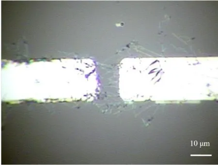
Figure 4. (a) Layout of the metal electrodes. Nine pairs of electrodes were patterned on a glass substrate using the lift-off process with a pitch of 4 mm between the adjacent electrodes. (b) Photographs of the tip of each electrode. The size of the gap between the pair of electrodes was 10 μm.
3.2. Assembly of nanowire sensors by means of DEP force
[image:7.596.61.536.211.405.2] [image:7.596.185.410.538.708.2]
DEP force was used to assemble the Si nanowires on the metal electrodes. First, 10 μL of IPA solution with Si nanowires was dripped onto the electrodes. Based on reports in the literature [31], IPA was chosen as the dispersion medium, rather than deionized water or ethanol. The torque exerted on the nanowire was only slightly different from the aforementioned three solvents; however, the generated DEP force was the largest in the IPA solution than for the other two solvents. Then, an AC voltage with an amplitude of 10 Vpp and a frequency of 100 kHz was applied to the metal electrodes. At this frequency, Si nanowires experience a small electroosmotic fluid velocity and high positive DEP force [32,33]. The assembly process was observed in real time using the CCD to control the number of nanowires that bridged the gap between each pair of electrodes. It can be observed that the nanowires were attracted onto the metal electrodes by the positive DEP force; however, based on our observation, it was difficult to observe nanowires of less than 100 nm in diameter under an optical microscope. Therefore, the number of nanowires bridging the gap between each pair of electrodes is only a subjective estimate. Note that not all of the nanowires were perfectly aligned between the electrode gap. The orientation of the assembled nanowire depends on its initial position and orientation as well as the gap size between the electrodes and the length of the nanowires. The details of the underlying physics of the DEP-manipulated nanowires including the DEP force and torque as well as the hydrodynamic drag force and torque have been previously reported in the literature [34]. After the nanowires bridged the gap, the nanowires were only adhered onto the electrodes physically. Thus, the nanowires were in contact with the metal electrodes to varying degrees and the contact resistance between the nanowires and the metal electrodes was high. As a result, the electric stability of the sensor was low, and the overly high contact resistance was also unfavorable for sensing applications. Therefore, a second photolithography process and deposition of a second layer of Ni were performed to fix the nanowires. Before the second nickel layer was deposited, the aligned nanowire was cleaned in an O2 plasma chamber, as described in Section 2.2. Then, the photoresister S1818 was spin-coated
concentration of the nanowire solution.
3.3. Characterization of the electrical properties of Si nanowires
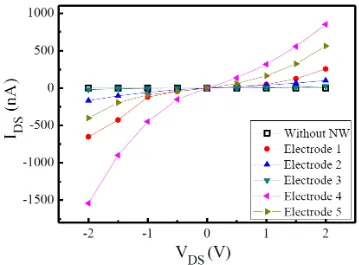
Figure 6. The I-V characteristics of the nanowire sensors before the nanowires were sandwiched between two metal layers, which revealed the Schottky contact property. The applied potential range was from -2 V to 2 V, with a semiconductor characterization system (Keithley 4200-SCS).
After the nanowire sensors were assembled, a Keithley 4200 semiconductor parameter analyzer was used to measure their IDS-VDS characteristic curves. The applied potential range was from -2 V to
2 V, with an interval of 0.5 V. Figure 6 shows the IDS-VDS curves of the nanowires arranged on the
electrodes only by the DEP force, which were measured after the IPA solution had evaporated. As mentioned above, the assemble yield rate cannot be 100% because failure may occur during the DEP assembling process, the cleaning process, or the photolithography aligning process. Only the nanowires in which the electrical properties were measurable were taken into account for the data reveal. There were five nanowires that were successfully connected after the second lift-off process in nine pairs of electrodes. Therefore, we chose five pairs of electrodes to study the electrical properties before and after the second lift-off process. In terms of the electrical properties of the un-clipped nanowires, similar trends can be found for the IDS-VDS curves of the nanowires on the five pairs of
electrodes: each curve is symmetrical around the origin and the curve is not linear. It is speculated that such trends occurred because the nanowires and the metal electrodes were only in physical contact with one another, thereby forming a Schottky contact between them. Because of the difference in the number of nanowires bridging the electrodes among the five pairs of electrodes, the five IDS-VDS
[image:9.596.117.476.146.411.2]
black hollow squares signifies the IDS-VDS curve measured when no nanowires were present between
the electrodes; this curve is used as the reference signal. To improve the contact resistance between the nanowires and the metal electrodes, a second lift-off process was performed to deposit a second layer of metal at the locations where the two ends of the nanowires came in contact with the first layer of metal to form a metal/nanowire/metal structure at the two ends of the nanowires.
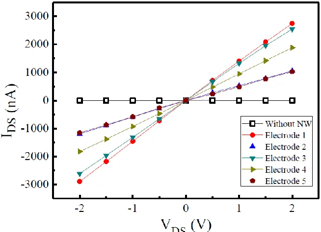
Figure 7. The I-V characteristics of the nanowire sensors after the nanowires were fixed between two metal layers, which exhibited an ohmic contact property. The applied potential range was from -2 V to 2 V, with an interval of 0.5 V.
Figure 7 shows the IDS-VDS curves measured after the second layer of metal was deposited. It
[image:10.596.135.462.179.416.2]
consistent, which demonstrates that nanowires assembled using this method can be used as biosensors in the future.
4. CONCLUSIONS
A DEP force generated by electrostatic attraction can rapidly attract nanowires to bridge the metal electrodes, providing a convenient nanowire assembly method that requires a relatively simple experimental setup. The number of assembled nanowires can be approximately controlled by controlling the duration of application of the AC voltage. If the number of assembled nanowires must be precisely controlled, the width of the metal electrodes may need to be reduced to 1–2 µm to avoid an overly large DEP force-affected area. It was also found that the electrical properties of the devices could be stabilized by fixing the nanowires, which was achieved by clamping them onto the upper and lower metal electrodes. In subsequent studies, clamped devices may be subjected to thermal annealing to observe whether this treatment can further improve the contact resistance between the nanowires and the metals. In the future, the modification of antibodies or other biorecognizers on nanowires will be conducted to achieve high-sensitivity label-free biosensors, which are advantageous due to their high surface-to-volume ratios.
ACKNOWLEDGMENTS
We would like to thank Prof. Yit-Tsong Chen from National Taiwan University for providing the silicon nanowires and offering valuable suggestions. We also express our gratitude to the Ministry of Science and Technology of Taiwan and the Chang Gung Memorial Hospital for their financial support (MOST 103-2221-E-182-016-MY2, CMRPD2C0091, BMRPC01).
References
1. S. Iijima, Nature, 354 (1991) 56.
2. J. C. Shin, P. K. Mohseni, K. J. Yu, S. Tomasulo, K. H. Montgomery, M. L. Lee, J. A. Rogers and X. Li, ACS Nano, 6 (2012) 11074.
3. Y. Hu, R. R. LaPierre, M. Li, K. Chen and J.-J. He, J. Appl. Phys., 112 (2012) 104311.
4. L.-C. Qin, X. Zhao, K. Hirahara, Y. Miyamoto, Y. Ando and S. Iijima, Nature, 408 (2000) 50. 5. M. Han, S. Liu, L. Zhang, C. Zhang, W. Tu, Z. Dai and J. Bao, ACS Appl. Mater. Interfaces, 4
(2012) 6654.
6. Y. Cui, Z. Zhong, D. Wang, W. U. Wang and C. M. Lieber, Nano Lett., 3 (2003) 149. 7. Y. Cui, Q. Wei, H. Park and C. M. Lieber, Science, 293 (2001) 1289.
8. W. Lu, P. Xie and C. M. Lieber, IEEE Trans. Electron Devices, 55 (2008) 2859.
9. B. P. Timko, T. Cohen-Karni, Q. Qing, B. Tian and C. M. Lieber, IEEE Trans. Nanotechnol., 9 (2010) 269.
10.K.-I. Chen, B.-R. Li and Y.-T. Chen, Nano Today, 6 (2011) 131.
11.R. G. Hobbs, N. Petkov and J. D. Holmes, Chem. Mat., 24 (2012) 1975. 12.W. Lu and C. M. Lieber, Nat. Mater., 6 (2007) 841.
14.W. S. Wong, S. Raychaudhuri, R. Lujan, S. Sambandan and R. A. Street, Nano Lett., 11 (2011) 2214.
15.R. Sharma and M. S. Strano, Adv. Mater., 21 (2009) 60.
16.Z. Wang, R. Bao, X. Zhang, X. Ou, C. S. Lee, J. C. Chang and X. Zhang, Angew. Chem.-Int. Edit., 50 (2011) 2811.
17.S. Raychaudhuri, S. A. Dayeh, D. Wang and E. T. Yu, Nano Lett., 9 (2009) 2260. 18.Z. Hu, M. D. Fischbein, C. Querner and M. Drndić, Nano Lett., 6 (2006) 2585.
19.K. M. Ryan, A. Mastroianni, K. A. Stancil, H. Liu and A. P. Alivisatos, Nano Lett., 6 (2006) 1479. 20.E. M. Freer, O. Grachev, X. Duan, S. Martin and D. P. Stumbo, Nat. Nanotechnol., 5 (2010) 525. 21.C. H. Lee, D. R. Kim and X. Zheng, Nano Lett., 10 (2010) 5116.
22.D.-I. Suh, S.-Y. Lee, J.-H. Hyung, T.-H. Kim and S.-K. Lee, J. Phys. Chem. C, 112 (2008) 1276. 23.S.-W. Lee, G. Jo, T. Lee and Y.-G. Lee, Opt. Express, 17 (2009) 17491.
24.A. Jamshidi, P. J. Pauzauskie, P. J. Schuck, A. T. Ohta, P.-Y. Chiou, J. Chou, P. Yang and M. C. Wu, Nat. Photonics, 2 (2008) 86.
25.J. Westwater, D. P. Gosain, S. Tomiya, S. Usui and H. Ruda, J. Vac. Sci. Technol. B, 15 (1997) 554. 26.T.-W. Lin, P.-J. Hsieh, C.-L. Lin, Y. Fang, J.-X. Yang, C.-C. Tsai, P.-L. Chiang, C.-Y. Pan and
Y.-T. Chen, Proc. Natl. Acad. Sci. U. S. A., 107 (2010) 1047.
27.F. Patolsky, G. Zheng and C. M. Lieber, Nat. Protoc., 1 (2006) 1711.
28.C.-C. Lin, S.-Y. Wang, W.-L. Lin, Y.-L. Lin, C. Cheng, W.-H. Sun, Z.-L. Chen, C.-H. Chien and F.-H. Ko, Int. J. Electrochem. Sci., 10 (2015) 7192.
29.W. M. Weber, L. Geelhaar, A. P. Graham, E. Unger, G. S. Duesberg, M. Liebau, W. Pamler, C. Chèze, H. Riechert, P. Lugli and F. Kreupl, Nano Lett., 6 (2006) 2660.
30.C. Opoku, K. F. Hoettges, M. P. Hughes, V. Stolojan, S. R. P. Silva and M. Shkunov, Nanotechnology, 24 (2013) 405203.
31.L. Yao, Y. Cui, H. Cong, J. Zheng, M. Shang, Z. Yang, W. Yang, G. Wei and F. Gao, J. Nanosci. Nanotechnol., 16 (2016) 3925.
32.A. W. Maijenburg, M. G. Maas, E. J. B. Rodijk, W. Ahmed, E. S. Kooij, E. T. Carlen, D. H. A. Blank and J. E. ten Elshof, J. Colloid Interface Sci., 355 (2011) 486.
33.M. Constantinou, K. F. Hoettges, S. Krylyuk, M. B. Katz, A. Davydov, G.-P. Rigas, V. Stolojan, M. P. Hughes and M. Shkunov, Appl. Phys. Lett., 110 (2017) 133103.
34.Q. Tao, F. Lan, M. Jiang, F. Wei and G. Li, J. Nanopart. Res., 17 (2015) 306.
35.I. B. Alicia, J. B. Joseph, A. B. Kris and M. B. Victor, Nanotechnology, 23 (2012) 245301.
36.M. Collet, S. Salomon, N. Y. Klein, F. Seichepine, C. Vieu, L. Nicu and G. Larrieu, Adv. Mater., 27 (2015) 1268.
37.C. Leiterer, G. Broenstrup, N. Jahr, M. Urban, C. Arnold, S. Christiansen and W. Fritzsche, J. Nanopart. Res., 15 (2013) 1628.
38.Z. Wang, M. Kroener and P. Woias, Sens. Actuator A-Phys., 188 (2012) 417.