Int. J. Electrochem. Sci., 8 (2013) 6767 - 6774
International Journal of
ELECTROCHEMICAL
SCIENCE
www.electrochemsci.org
Structural and Optical Properties of a bi-Structured ZnO Film
Prepared Via Electrodeposition
N. H. Al-Hardan1,*, Azman Jalar1, M.A. Abdul Hamid2, Lim Karkeng2 and R. Shamsudin2
1
Institute of Microengineering and Nanoelectronics (IMEN)
2
Faculty of Science & Technology; Universiti Kebangsaan Malaysia (UKM); 43600 Bangi; Selangor, Malaysia
*
E-mail: [email protected]
Received: 10 March 2013 / Accepted: 31 March 2013 / Published: 1 May 2013
This study reports the fabrication of a bi-structured zinc oxide (ZnO) film via electrodeposition onto conductive coated glass. The produced ZnO film exhibits a polycrystalline nature with preferential orientation toward the c-axis. Scanning electron microscopy (SEM) images of the film show the presence of two structures: the bottom layer consisted of sub-micron particles with a hexagonal structure, and plate-like structures of ZnO grew on the top of the hexagonal particles. The ZnO exhibited a weak emission in the UV band and no visible emissions were observed. Blue and red emissions appeared at 2.83 eV and 1.63 eV, respectively, and were attributed to the defect concentrations of oxygen interstitials and zinc vacancies.
Keywords: A. Semiconductors; B. Chemical synthesis; D. Crystal structure; D. Defects; D.
Luminescence
1. INTRODUCTION
method has received increased attention for the production of ZnO films; its advantages include being simple, inexpensive, and suitable for large-area substrates. The process uses zinc chloride (ZnCl2) or
zinc nitrate Zn(NO3)2 as a precursor [11]. The method utilises a low cathode voltage or current to
produce the ZnO films on any conductive substrate [12]. The method generates hydroxide ions at the surface of an electrode through the cathodic reduction of the oxygen precursor. The main oxygen source for this reaction is dissolved molecular oxygen or nitrate ions [13]. The structures of the prepared ZnO films can be tailored by controlling the deposition parameters, such as the precursor concentrations, applied voltages, the temperature of the solution and the substrates used [14, 15].
The photoluminescence (PL) of ZnO has been intensively studied by several groups [16, 17]. The purpose of these studies was to elucidate the origin of different emission bands that are related to different origins of the defects in ZnO [16]. The emissions of ZnO are affected by different preparation conditions, such as the oxygen pressure, the growing temperature [18], the post-annealing temperature and the use of different atmospheric gas annealing processes [19, 20]. Recently, the effect of different deposition time at a constant current (2 mA.cm-2) show the growth of bi – strictures of the ZnO prepared via cathodic electrodeposition method. The SEM results show the growth of a 2D plate like structures fallows by the grown of urchins like structure [21].
Despite several published works that address the electrodeposition process, few of the published studies involve a high cathodic voltage. In this work, we report the growth of ZnO films at a high cathodic voltage. The resulting film exhibits bi-structure morphology. The structural and optical properties of the ZnO films produced using the electrodeposition method are investigated.
2. EXPERIMENTAL DETAILS
Bi-structured ZnO thin films were prepared via an electrodeposition method on a glass-slide substrate coated with a conductive layer of indium tin oxide (ITO) (BSJ Group, China). The sheet resistance of the ITO was approximately 20 /sq. The glass slide was cut into pieces with dimensions of 1.0 × 1.5 cm2
and was cleaned using ultrasonic cleaning method. Acetone, ethanol, and deionized water were used for this process, and then the glass slides were dried in flow of air. The electrolyte was an aqueous solution of zinc chloride (ZnCl2), which served as a zinc source, and potassium chloride
(KCl) to ensure good conductivity in the aqueous solution; both compounds were reagent grade and were obtained from Merck. The aqueous solution was prepared using a 15 mM ZnCl2 and a 0.1 M KCl
both salts were dissolved in 100 ml of deionised water (resistance ~ 18 M).
was applied to the working electrode, the reaction was initiated. The deposition reaction in the electrolyte can be written as [10]:
2
2
1
2 (1) 2
Zn O e ZnO
The growth time was fixed at 90 minutes. An Agilent E3631A DC power supply was used as a voltage source. The produced sample was carefully rinsed with deionised water to remove the chloride salts and was subsequently dried on a hot plate at 80 °C for 15 minutes. The prepared film was post-annealed at 500 °C for 1 hr under ambient atmospheric conditions in a controllable tube furnace.
The surface morphology and the phase structure of the ZnO film were investigated using scanning electron microscopy (SEM), which was conducted on a Zeiss LEO 1450VP scanning electron microscope. Energy-dispersive X-ray spectroscopy (EDX, Oxford Inca) was performed to determine the elemental composition. X-ray diffraction (XRD, Bruker D8 ADVANCE) was used to identify the phase structures. The XRD unit was equipped with a copper (Cu) target that emits X-rays with a wavelength of 0.154 nm at an operating voltage of 60 kV and a current of 60 mA. For the optical emission measurements, the photoluminescence (PL) spectrum was recorded using an Edinburgh Photonics FLS920 equipped with a xenon lamp (450 W). The measurement range was 320 to 800 nm, and the excitation wavelength was 300 nm. All the measurements were performed under atmospheric conditions (21 °C and 50% relative humidity).
3. RESULTS AND DISCUSSION
3.1. The morphology and structure of the produced ZnO films
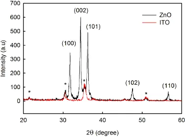
The XRD pattern of the prepared ZnO film is depicted in Fig (2). The diffraction peaks related to the ITO-coated glass are indicated with an asterisk (∗). The pattern proves the polycrystalline nature of the produced ZnO. According to JCPDS card 036-1451, the resulting patterns matched well with that of the hexagonal (wurtzite) crystal structure of the ZnO
[image:4.596.121.486.160.433.2]
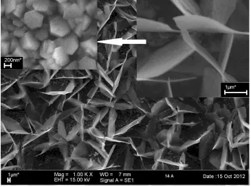
Figure 1. The morphology of the ZnO film produced at a cathodic voltage of -2.2 V. The bottom area
shows the total area, the upper right-hand side shows the 2D plate-like structure (the bar length represents 1 micron), and the upper left-hand side shows the hexagonal particles (the bar length represents 200 nm).
The peaks of the ZnO film appeared at Bragg angles of 31.78°, 34.43°, 36.25°, 47.58° and 56.63°; these peaks represent the (100), (002), (101), (102) and (110) phases, respectively, of the hexagonal structure of ZnO (JCPDS 036-1451).
The high intensity of the peaks demonstrates the high quality of the produced ZnO film. The most intense peak in the XRD pattern is the (002) reflection, which indicates that the ZnO grew parallel to the c-axis of the hexagonal structure.
The XRD results agree with the SEM image, which shows that the bottom layer consisted of hexagonal particles that grew perpendicular to the surface. The plate-like structures grew horizontal to the c-axis, which resulted in the (100) and (101) reflections in the XRD pattern of the structure. The lattice constants (a and c) of the hexagonal structure can be calculated from the following relationship [23]:
2 2 2
2 2 2
( )
1 4
( ) (2) 3
hkl
h hk k l
where d(hkl) represents the lattice spacing, and h, k and l are the Miller indices. The results indicate that a = 3.250 nm and c = 5.2094 nm. Both of these values are in good agreement with the lattice constants reported in the JCPDS database (a = 3.24982 nm and c = 5.20661 nm).
X-ray profile analysis allowed the microstructural characterisation of the produced ZnO film to be investigated based on the broadening of the peaks. The microstrain () and crystallite size (D) can be calculated from the corresponding Williamson–Hall (W–H) plot with the following relation [24, 25]:
cos 1 sin
(3)
D
where and represent the Cu wavelength (0.154 nm), the full-width at half-maximum (FWHM) of the peak and the Bragg angle, respectively. As evident from Eq. (3), a plot of cos
against sin
[image:5.596.91.468.414.694.2] will result in a straight line, where the intercept on the Y-axis reveals the particle size that corresponds to zero strain; the strain is determined from the slope of the line. The results show that the mean crystallite size and the microstrain of the prepared ZnO were 33 nm and 29.8 × 10⁻³, respectively.
Figure 2. The XRD pattern of the produced ZnO film. The asterisks (*) denote peaks attributed to the
The composition analysis via EDX for both structures indicated the presence of only Zn and O. The atomic percentages of Zn and O were 46.57% and 53.43%, respectively, for the 2D plate-like structure, whereas they were 48.34% and 51.66%, respectively, for the hexagonal particles. The ratio of the Zn:O in the 2D plate structure was higher than the bottom one.
3.2. Emission properties
[image:6.596.78.467.310.596.2]The room-temperature PL spectrum of the prepared ZnO thin film on an ITO glass substrate collected under an excitation wavelength of 300 nm is depicted in Fig. (3). The spectrum shows weak UV emission peaks at approximately 3.24 eV (382 nm) and 3.13 eV (396 nm). These two weak peaks may be attributed to the two-phonon replicas due to two transverse optical phonons with a separation of ~ 108 meV [16]; this value agrees with that in the study case.
Figure 3. The PL spectrum of a ZnO film grown on ITO glass at room temperature.
experimentally using the electroluminescence measurements of undoped ZnO [17]. The result of this transition is consistent with the photon energy of the blue emission observed in this study (2.83 eV).
Another weak emission was observed at 2.66 eV, which resulted from the Vzn [16]. The last
emission band was a strong emission (red-NIR) at 1.62 eV. This emission has been rarely observed in the PL spectra of pure ZnO [16]. The red line emission was attributed to the superposition of emissions related to the oxygen Oi and VO [17].
The emissions that arise from the defect levels in ZnO result from extremely complex processes and are still not fully understood. Nevertheless, in this study, it is suggested that the zinc vacancies and oxygen interstitials were responsible for the origin of this band; as confirmed by the absence of the green–yellow band, the oxygen vacancies were limited. Moreover, this explanation is in agreement with the EDX results of the prepared ZnO samples, as was previously discussed. This work is still in progress to complete the study.
4. CONCLUSION
Bi-structured ZnO films were electrodeposited onto ITO glass. The cathodic voltage was fixed at -2.2 V, and the reaction time was fixed at 90 minutes. The XRD pattern of the produced layers indicated the polycrystalline nature of the films. Furthermore, the SEM images reveal the bi-structural nature of the ZnO. The bottom structures were highly dense hexagonal particles, and plate-shaped structures grew on top of this base layer. The photon emissions of the produced ZnO film was in the near-UV band (3.26 eV). Blue emission was observed at 2.83 eV, and the last emission was observed at 1.63 eV; this last emission) that is an IR–NIR-band emission.
ACKNOWLEDGEMENT
This work was supported by the Universiti Kebangsaan Malaysia (UKM) through the short-term grants OUP-2012-120 and DIP-2012-2014. The authors are also thankful to the Centre for Research and Instrumentation Management (CRIM) at UKM for providing the PL measurements and VPSEM.
References
1. H. Morkoç, Ü. Özgür, Zinc Oxide: Fundamentals, Materials and Device Technology, WILEY-VCH Verlag GmbH & Co. KGaA, Weinheim, 2009.
2. U. Ozgur, Y.I. Alivov, C. Liu, A. Teke, M.A. Reshchikov, S. Dogan, V. Avrutin, S.J. Cho, H. Morkoc, J. Appl. Phys. , 98 (2005) 041301-041103.
3. Z.L. Wang, ACS Nano, 2 (2008) 1987-1992.
4. W. Zhong Lin, J. Phys.-Condes. Matter 16 (2004) R829.
5. J. Zhong, Y. Lu, ZnO-Based Ultraviolet Detectors, in: C.W. Litton, T.C. Collins, D.C. Reynolds, P. Capper, S. Kasap, A. Willoughby (Eds.) Zinc Oxide Materials for Electronic and Optoelectronic Device Applications, John Wiley & Sons, 2011.
6. M.H. Huang, S. Mao, H. Feick, H. Yan, Y. Wu, H. Kind, E. Weber, R. Russo, P. Yang, Science, 292 (2001) 1897-1899.
8. T.-J. Hsueh, C.-L. Hsu, Sens. Actuator B-Chem. , 131 (2008) 572-576.
9. S.N.F. Hasim, M.A. Abdul Hamid, R. Shamsudin, A. Jalar, J. Phys. Chem. Solids, 70 (2009) 1501-1504.
10. T. Pauporté, D. Lincot, Electrochim. Acta, 45 (2000) 3345-3353. 11. S. Xu, Z. Wang, Nano Res., 4 (2011) 1013-1098.
12. L. Yu, G. Zhang, S. Li, Z. Xi, D. Guo, J. Cryst. Growth, 299 (2007) 184-188. 13. T. Pauporté, D. Lincot, J. Electroanal. Chem., 517 (2001) 54-62.
14. A. Goux, T. Pauporté, J. Chivot, D. Lincot, Electrochim. Acta, 50 (2005) 2239-2248. 15. H. Kim, J.Y. Moon, H.S. Lee, Electron. Mater. Lett., 5 (2009) 135-138.
16. A.B. Djuriscaroni, Y.H. Leung, Small, 2 (2006) 944-961.
17. N.H. Alvi, K.u. Hasan, O. Nur, M. Willander, Nanoscale Res. Lett., 6 (2011) 130. 18. D.H. Zhang, Z.Y. Xue, Q.P. Wang, J. Phys. D-Appl. Phys., 35 (2002) 2837. 19. Y.F. Hsu, A.B. Djurišić, K.H. Tam, J. Cryst. Growth, 304 (2007) 47-52.
20. X.Q. Wei, B.Y. Man, M. Liu, C.S. Xue, H.Z. Zhuang, C. Yang, Physica B, 388 (2007) 145-152. 21. N.H. Al-Hardan, M.A.A. Hamid, A. Jalar, L. Karkeng, R. Shamsudin, B.Y. Majlis, Int. J.
Electrochem. Sci., 8 (2013) 2430 - 2439.
22. F. Wang, R. Liu, A. Pan, L. Cao, K. Cheng, B. Xue, G. Wang, Q. Meng, J. Li, Q. Li, Y. Wang, T. Wang, B. Zou, Mater. Lett., 61 (2007) 2000-2003.
23. O. Lupan, T. Pauporté, L. Chow, B. Viana, F. Pellé, L.K. Ono, B. Roldan Cuenya, H. Heinrich, Appl. Surf. Sci., 256 (2010) 1895.
24. M. Birkholz, Thin Film Analysis by X-Ray Scattering, WILEY-VCH Verlag GmbH, 2006. 25. S.K. Mishra, R.K. Srivastava, S.G. Prakash, J. Alloy. Compd., 539 (2012) 1–6.
26. X. Wei, B. Man, C. Xue, C. Chen, M. Liu, Jpn. J. Appl. Phys., 45 (2006) 8586.