Int. J. Electrochem. Sci., 7 (2012) 1359 - 1370
International Journal of
ELECTROCHEMICAL
SCIENCE
www.electrochemsci.org
The Analysis of the Deposition Rate for Continuous
Micro-Anode Guided Electroplating Process
Yean-Ren Hwang1, , Jing-Chie Lin1,2,* , Ting-Chao Chen1 1
Department of Mechanical Engineering, National Central University, No 300, Jhongda Rd, Jhongli City, Taoyuan County 320, Taiwan, Republic of China
2
Institute of Materials Science and Engineering, National Central University, No.300, Jhongda Rd., Jhongli City, Taoyuan County 320, Taiwan, Republic of China
*
E-mail: [email protected]
Received: 26 November 2011 / Accepted: 4 January 2012 / Published: 1 February 2012
The continuous micro-anode guided electroplating (MAGE) has been improved by using real time control of anode’s elevation rate based on CCD images in the previous research. However, the effects of choosing different process parameters, such as the applied voltage and the gap distance between the anode and column, had not been fully discussed in the previous work. In order to manage the electroplating process and obtain the desired column, the relations between the column’s geometry and the process parameters are investigated in this paper. The experiment results show that the deposition rate is related to the gap distances as well as the applied voltages. By implementing the system identification and curve fitting techniques, the transfer functions between the applied voltage and the column deposition rates are established for different gap distances. Based on these functions and the on-line CCD images, the anode position and the applied voltage will be adjusted real time to maintain constant gap distance and obtain the desired column geometries.
Keywords: electroplating, CCD image, system identification, real time control
1. INTRODUCTION
dynamic relationship between the input voltage and the column’s deposition rate, which will determine the physical dimension of the column, had not been systematically discussed in Chen’s previous paper. Hence, for a desired dimension, engineers cannot easily find the suitable input voltage and the anode moving rate.
The various bias voltage conditions, the concentration of copper sulfate and the organic additives can make the critical gap, the micro-structure and current efficiency different in the intermittent electroplating process [9-12]. In addition, the issue of the ratio of linear relationship of the diameters of the micro anode and the deposit micro-column becomes one to one had also been discussed [13,14]. Some intermittent plating process installs imaging devices as monitoring systems, however, relevant image processing techniques and methods are not effectively used to achieve the purpose of feedback control to micro-plating system nowadays[15-17].
As for the continuous electroplating process, to modify and improve the physical properties of the micro-structure, a process of Deposition-Detection-Withdrawal (DDW) and the way of assuming fixed deposition rate to continuously maintain certain gap distance had both been discussed[18-20]. However, with the lack of feedback signals, the method of assuming fixed deposition rate cannot accurately maintain the gap distance and thus cannot produce well formed micro-structure.
In order to assist users, the hardware set up is described in Section 2, the process parameters and the depositing rate for different input voltages are discussed and analyzed in this paper followed by Section 2. Besides, the effect of the gap between anode-cathode, which is used for feedback control the anode rate, is also discussed in Section 3. Furthermore, the experiment results are discussed in Section 4 and the conclusion is stated in Section 5 respectively. Hardware Setup
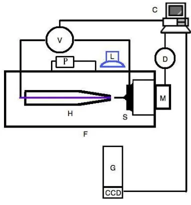
[image:2.596.191.382.519.724.2]In this paper, a real-time guided continuous micro-electroplating system consists of the image hardware system and the micro-electroplating system is developed and proposed. The control unit of this system, computer, is used to control and achieve the continuous micro-electroplating function with the proposed software.
[image:3.596.134.463.300.537.2]
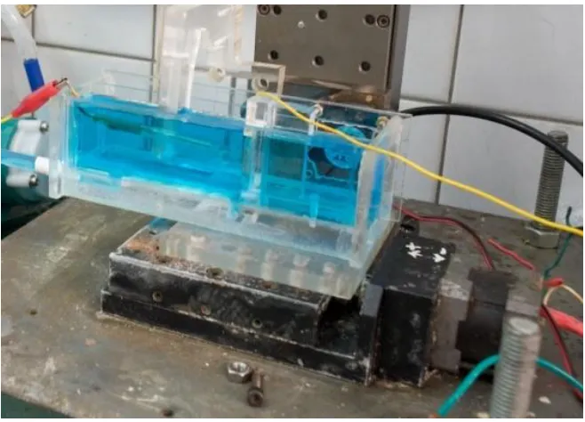
The image hardware system includes the computer (C), the magnifier lens (G) and the CCD camera (CCD). The images are processed and recognized for taking anode-cathode distance to achieve the continuous micro-electroplating function and produce the copper columns are captured by a CCD camera with magnifier lens and are transported to the computer by video capture card. The micro-electroplating system, as shown in Figure 1, whereas contains the micro-stepping motor (M), the micro-stepping motor driver (D), the micro-anode (H), the cathode (S), the electrical power supplier (V), the depositing cell (F), the pump (P), and the high-power LED module (L). The micro-anode of the electroplating system is made of platinum wire with the diameter of 125 um and put it to a bakelite tube with cold-mounted resin. The cathode is made of pure copper and the depositing cell is constructed with PolyMethyl MethAcrylate (PMMA). Eventually, the micro-anode and cathode are put into the depositing cell which uses a typical sulfate bath with the 0.8M CuSO4‧5H2O and 0.65M H2SO4, as shown in Figure 2.
Figure 2. The depositing cell
[image:4.596.143.453.145.367.2]
However, the mentioned hardware above is critically controlled by the software, and the software process parameters and the experimental method will be further discussed in the following section.
Figure 3. The hardware system diagram
2. THE ANALYSIS OF THE COPPER MICRO-COLUMN’S DEPOSITION RATE
Three different gap distances- 7, 9 and 11 pixels, between the micro-anode and the copper column and five input voltages- 3.1, 3.2, 3.3, 3.4 and 3.5 are applied as variable parameters to analyze the deposition rate of the copper columns. The temperature of sulfate solution and the erroneous judgment of the image processing are represented as fixed parameters in this experiment. The temperature of sulfate solution is maintained at room temperature, 20 degrees Celsius, and the image measurement tolerance is set plus or minus one pixel of the set anode-cathode distances. The sample in time is 1 Hz to do image processing and to observe its deposition conditions. The deposition rate of the copper micro-column and the approximation curve will be further discussed in the following paragraph.
2.1. The deposition rate of the copper micro-column
Figure 4. Length and diameter algorithms
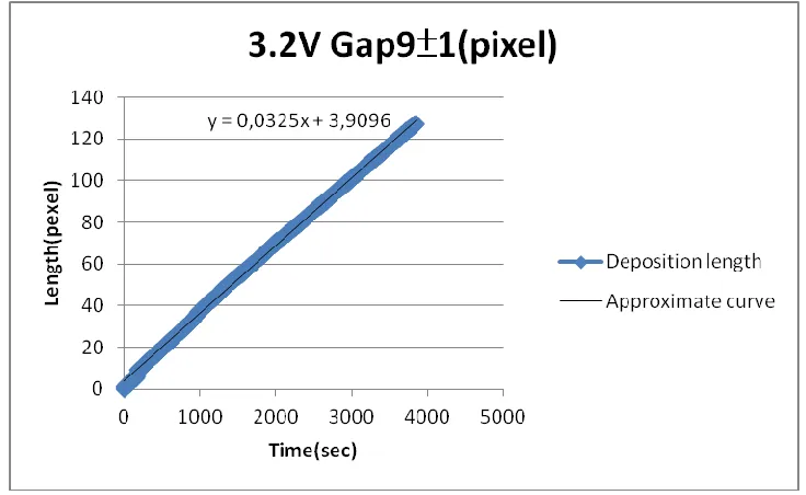
The deposition rate of copper column’s length varies on the combinations of input voltages and gap distances. By processing and analyzing the captured images, a linear relationship is reported between the deposition length of the copper micro-column and the time, as shown in Figure 5.
Figure 5. The graph of deposition length and time(Voltage 3.2v & Gap9±1 )
The deposition rate of copper column length, as shown in Figure 5, is applying the value of its deposition length to figure the slope of the approximate curve. The linear equation of the deposition length is represented as Formula 1.
[image:5.596.114.482.362.588.2][image:6.596.146.455.185.436.2]
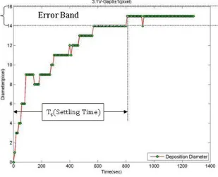
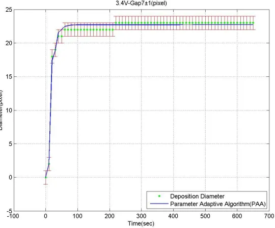
At different applied voltages and gap distances, the maximum deposition diameter of the copper micro-column will be developed. Within the mentioned image measurement tolerance range (Error Band), the system is regarded the steady deposition time of the produced maximum diameter as the settling time, as shown in Figure 6. The deposition rate of the copper column at the various input voltages and gap distances will be examined in detail in the following section.
Figure 6. The response of the system
2.2. Parameter Adaptive Algorithm Identification
The deposition rate of the copper micro-column length can be expressed by simple linear equations. As its length grows higher, the deposition rate will slow down and become steady. The Z-transform is obtained from system identification, as shown in equation 2. Where the input “u” is for the step voltage, output “y” is for the deposition diameter of the copper micro-column calculated by the image processing method.
(2)
transpose equation 2 into equation 3;
then do the anti-Z on the equation 3 into equation 4, 5, 6;
(4)
(5)
where “K” is for the data sequence of the deposition diameter of the copper column; “ai” and “bj” represent the values of the transform function and “n” is for the system order;
, , (6)
then the use of the least squares method, as shown in equation 7;
(7)
where ”N” is for the number of the data of the deposition diameter of copper column, “y(i)” is for the value of each deposition diameter, “ ” is for the value of each data from system identification. Then use the method of partial differential to obtain matrix as “J” is the minimum value, as shown in Formula 8;
(8)
Parameter Adaptive Algorithm(PAA) is a kind of system identification which can obtain each factor of the transfer function G (z) in Formula 8.
3. RESULTS AND DISCUSSION
3.1 The analysis of the deposition rate of the copper micro-column length
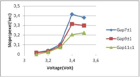
rate, as mentioned above, can be perceived at three different gap distances and five applied voltages. According to the experiment results, the fastest deposition rate of the copper column length is at voltage 3.4 and gap distance 7±1 pixels. In other words, the higher voltage and the smaller gap distance can fasten the deposition rate. Theoretically, in the same gap distance, the deposition rate of the copper column at voltage 3.5 should be faster than it at voltage 3.4. Unfortunately, the result does not come out fairly as the normal assumption. That is because the over high voltage, over small gap distance and more bubbles enhance the error estimation of the gap distance images. Because of the error estimation of images, the system keeps moving micro-anode to maintain the appropriate gap distance, and then cause the instability of the electric field and lower the deposition rate of the copper micro-column length. Thus, at voltage 3.5, the use of gap distance 11±1 pixels can better avoid the decrease of the deposition rate. Worth to be mentioned, at voltage 3.1 and gap distance 11±1 pixels, the copper micro-column cannot be formed properly because of the over small voltage and the over big gap distance.
[image:8.596.154.444.318.480.2]Figure 7. The diagram of the slope of different voltages and gap distances
Table 1. The table of the slope at different voltages and gap distances
Gap Voltage
7±1(pixel) 9±1(pixel) 11±1(pixel)
3.1(V) 0.0181 0.0157 X
3.2(V) 0.0375 0.0325 0.0234
3.3(V) 0.1031 0.0869 0.0731
3.4(V) 0.4152 0.3149 0.2054
3.5(V) 0.3812 0.2985 0.2248
the deposition length of the copper micro-column can be inference determined by the corresponding time.
3.2. The relationship between the electric field and the copper micro-column diameter
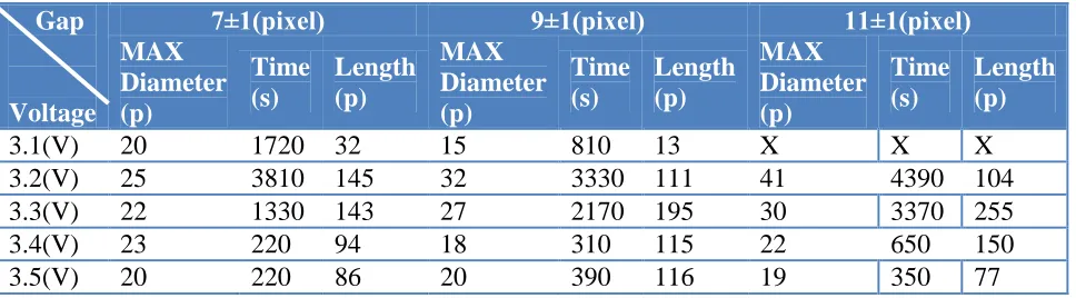
[image:9.596.59.543.411.545.2]As mentioned, the ratio of linear relationship of the anode and the micro-column becomes one to one. However, to form the relationship, certain gap distances and voltages are required. By observing the deposition diameter of the copper micro-column, the incidence of the electric field can be inference figured out. That is the time to produce the maximum diameter of the copper micro-column is the time to come off the incidence of the electric field. Basically, the electric field has its influential range. Higher voltages can strengthen the electric field intensity and also greaten the incidence of the electric field. The deposition rate of high voltage is too fast to keep the micro-anode constant, so that the electric field hardly can maintain stable. Yet, the electric field intensity of low voltage is too weak to have greater incidence of the electric field, so that the deposition diameter of the copper micro-column cannot be produced bigger. Thus, to obtain the desired diameter of the copper micro-column, the appropriate voltage and gap distance are requested.
Table 2. The relationship between the time and the maximum diameter at the voltages and the gap distances
Gap
Voltage
7±1(pixel) 9±1(pixel) 11±1(pixel)
MAX Diameter (p) Time (s) Length (p) MAX Diameter (p) Time (s) Length (p) MAX Diameter (p) Time (s) Length (p)
3.1(V) 20 1720 32 15 810 13 X X X
3.2(V) 25 3810 145 32 3330 111 41 4390 104
3.3(V) 22 1330 143 27 2170 195 30 3370 255
3.4(V) 23 220 94 18 310 115 22 650 150
3.5(V) 20 220 86 20 390 116 19 350 77
the copper micro-column cannot be well formed at voltage 3.1 and the gap distance 11±1 pixels, thus there is no relate experiment data can be analyzed.
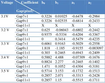
3.3. System identification
[image:10.596.129.470.343.613.2]The used system identification method can identify any order of the system. Calculate the transform functions of different orders respectively first, then compute sum of deviation with the estimated value of each step and the original data. It is found that there is no remarkable difference of the values of sum of deviation in second-order system and any other more complicated systems, thus the order system is used in this experiment. However, the transform functions of the second-order system are identified as Formula . The factors of the system are listed in Table 3 below.
Table 3. The factors of the transform function at various voltages and gap distances
Voltage Coefficient
Gap(pixel)
b0 b1 a1 a2
3.1V Gap7±1 0.3226 0.01025 -0.6478 -0.2984 Gap9±1 0.3226 0.02535 -0.6814 -0.2433
Gap11±1 X X X X
3.2 V Gap7±1 0.625 -0.06043 -0.6802 -0.2442 Gap9±1 0.9375 -0.5334 -0.6204 -0.3367
Gap11±1 0 0.3414 -0.5479 -0.4235
3.3 V Gap7±1 0.6061 0.9163 -0.5029 -0.2558 Gap9±1 1.818 -1.185 -0.9155 -0.003097 Gap11±1 0.303 0.2465 -0.6943 -0.2409 3.4 V Gap7±1 0.5882 4.488 -0.07309 -0.1676 Gap9±1 0.8824 2.277 -0.2465 -0.1402 Gap11±1 1.471 0.1052 -0.4304 -0.3181 3.5 V Gap7±1 0.5714 3.153 -0.1732 -0.1513 Gap9±1 0.2857 2.071 -0.3313 -0.2428 Gap11±1 0.2857 1.15 -0.5515 -0.1711
By applying the identified transform functions “ai” and ”bj” into Formula 9, the output value of the system can be calculated as “y”, the diameter of the copper micro-column.
(9)
[image:11.596.165.435.141.365.2]
Taking advantage of the identified approximation curve, the corresponding relationship to the deposition time and rate of the copper micro-column diameter can be analyzed clearly.
Figure 8. The comparison of the system identified transform function and original data
3.4. Future development and application
According to the experiment results, the deposition rate of the copper micro-column length is linearly growing with time. The fastest deposition rate of its length is obvious at voltage 3.4 and the gap distance 7±1 pixels. That is because the bubble issue at the voltage 3.4 doesn’t have serious impact on the image processing judgment. However, to deposit larger micro-copper column diameter, the certain input voltage and gap distance are required. In addition, the incidence of the electric field could be varied on the stability of the electric field.
In the paper, the deposition rate of copper micro-column and image processing feedback control can be used effectively to improve the unstable phenomenon of electric field influence in the future. The proposed linear equations of copper micro-column length and the system identified transform function of the copper micro-column diameter can further accurately and effectively estimate and control the deposition rate and size of the length and diameter of copper micro-column.
4. CONCLUSION
applied voltages and the gap distances. The deposition rates of the copper column length and diameter are not the same at various voltages and the gap distances. However, the various input voltages and the gap distances can be selected in the continuous electroplating process. Thus, by using various deposition rates of the copper column length and diameter, not only the desired copper column can be deposited, but the needed deposition time can be estimated.
References
1. J.D. Madden, S.R. Lafontaine and I.W. Hunter, Sixth International Symposium on Micro Machine and Human Science. (1995) 77.
2. J.D. Madden and I.W. Hunter, Journal of Microelectromechanical Systems. 5 (1996) 24. 3. I.W. Hunter, S.R. Lafontaine and J.D. Madden, US Patent 5,641,391 (1997)
4. R. A. Said, Nanotechnology 14(2003)523-531.
5. J. C. Lin, Y. S. Chen, C. F. Huang, J. H. Yang, T. K. Chang, Chung-Lin Wu, Y. R. Hwang and T. C. Chen, Int. J. Electrochem. Sci., 6 (2011) 3536 – 3549.
6. S.K. Seol, et. al., Electrochemical and Solid-State Letters, 7(9) (2004) C95-C97.
7. J.C. Lin, S.B. Jang, D.L. Lee, C.C. Chen, P.C. Yeh, T.K. Chang and J.H. Yang, J. Micromech. Microeng. 15 (2005) 2405.
8. T.C. Chen, Y.R. Hwang, J.C. Lin and Y.J. Ciou, Int. J. Electrochem. Sci., 5 (2010) 1810 – 1820. 9. E.M. El-Giar and D.J. Thomson, WESCANEX 97: Proc. IEEE Conf. Communications, Power and
Computing. (1997) 327.
10. E.M. El-Giar, R.A. Said, G.E. Bridges and D.J. Thomson, Journal of The Electrochemical Society. 147 (2000) 586.
11. S.K. Seol, J.M. Yi and X. Jin et al, Electrochemical and Solid-State Letters. 7 (2004) C95. 12. S.K. Seol, A.R. Pyun and Y. Hwu et al, Adv. Funct. Mater. 15 (2005) 934.
13. J.H. Choo, S.H. Yeo and F.F. Tan, Microsystem Technologies. 10 (2004) 127.
14. S.H. Yeo, J.H. Choo and K.S. Yip, In Micromachining and Microfabrication Process Technology VoI, 4174 (2000)30.
15. R.C. Gonzalez and R.E. Woods, Digital Image Processing, Prentice-Hall, New Jersey (2002). 16. R.C. Gonzalez, R.E. Woods and S.L. Eddins, Digital Image Processing using MATLAB,
Prentice-Hall, New Jersey(2003).
17. R.C. Gonzalez, R.E. Woods and S.L. Eddins, Digital I Image Processing using MATLAB, 2nd edition [Hardcover], Gatesmark Publishing. (2009).
18. C.S. Lin, C.Y. Lee, J.H. Yang and Y.S Huang, Electrochemical and Solid-State Letters, 8(9) (2005) C125–C129.
19. J.H. Yang, J.C. Lin, T.K. Chang, X.B. You and S.B. Jiang , J. Micromech. Microeng. 19 (2009) 12. 20. C.Y. Lee, C. S. Lin and B. R. Lin, J.Micromech. Microeng. 18 (2008) 105008 (8pp).