Theses Thesis/Dissertation Collections
9-2015
A Secure Neuromemristive Primitive to Mitigate
Correlation Power Analysis on SHA-3 Hash
Function
James B. Thesing
Follow this and additional works at:http://scholarworks.rit.edu/theses
This Thesis is brought to you for free and open access by the Thesis/Dissertation Collections at RIT Scholar Works. It has been accepted for inclusion in Theses by an authorized administrator of RIT Scholar Works. For more information, please [email protected].
Recommended Citation
Correlation Power Analysis on SHA-3 Hash
Function
by
James B. Thesing
A Thesis Submitted in Partial Fulfillment of the Requirements for the Degree of Master of Science
in Computer Engineering
Supervised by
Associate Professor Dr. Dhireesha Kudithipudi Department of Computer Engineering
Kate Gleason College of Engineering Rochester Institute of Technology
Rochester, New York September 2015
Approved by:
Dr. Dhireesha Kudithipudi, Associate Professor Thesis Adviser, Department of Computer Engineering
Dr. Marcin Łukowiak, Associate Professor
Committee Member, Department of Computer Engineering
Dr. Stanisław Radziszowski, Professor
Dedication
To my family, for their support and encouragement to get me to this point. To my wife,
Acknowledgments
I would like to thank my thesis adviser Dr. Dhireesha Kudithipudi for her guidance and
advice during my thesis work. I would like to thank Dr. Marcin Łukowiak for serving on
my committee and countless hours spent discussing power analysis techniques and
security issues. Also, I want to thank Dr. Stanisław Radziszowski for serving on my
committee and giving his time and guidance on my final thesis document.
I would also like to thank the members of the RIT Nano lab whose support, discussions
and presentations led to much of the success in this work: James Mnatzaganian, Dan
Christiani, Cory Merkel, Levs Dolgovs, Lennard Streat, Qutaiba Saleh and Abdullah
Zyarah. They are a great team to work with.
Finally, a special thank you to Xuan Tran. Our collaborative efforts were the basis of
figuring out the design flow and CPA attack methodology that led to both of our
Abstract
A Secure Neuromemristive Primitive to Mitigate Correlation Power Analysis on SHA-3 Hash Function
James B. Thesing
Supervising Professor: Dr. Dhireesha Kudithipudi
Passing messages to soldiers on the battle field, conducting online banking, and down-loading files on the internet are very different applications that all share one thing in com-mon, concerns over security of the data being processed. Data security depends on the cryptographic systems that take into account both the algorithmic weakness and the weak-nesses of the hardware devices they are implemented on. The current dominant hardware design medium is complementary metal-oxide-semi-conductor (CMOS). CMOS has been shown to leak more power as the technology node size decreases. The leaked power has a strong correlation with the bits being manipulated inside a device. These power leakages have brought on a class of power analysis that is able to extract secret information being processed in the algorithm with far less computational power than brute force guessing. Re-cently, many hardware designs have been proposed which have shown resistance against different forms of power analysis by changing hardware layouts; however, these designs are realized in the same technology, CMOS, that causes the side channel attack problem.
Contents
Dedication. . . ii
Acknowledgments . . . iii
Abstract . . . iv
1 Motivation . . . 1
2 Background . . . 3
2.1 Side Channel Attacks (SCA) . . . 3
2.2 Cryptographic Hash Functions . . . 3
2.3 Message Authentication Codes (MACs) . . . 5
2.4 Merkle-Damgard Vs. Sponge Hash Construction . . . 7
2.5 SHA-3 . . . 9
2.5.1 State XOR . . . 11
2.5.2 Theta (θ) . . . 12
2.5.3 Rho (ρ) . . . 12
2.5.4 Pi (π) . . . 14
2.5.5 Chi (χ) . . . 14
2.5.6 Iota (ι) . . . 16
2.6 Neuromorphic Computing . . . 17
2.7 Memristor Devices . . . 18
3 Supporting Work . . . 20
3.1 SCA with Power Analysis . . . 20
3.1.1 Simple Power Analysis (SPA) . . . 20
3.1.2 Differential Power Analysis (DPA) . . . 23
3.1.3 Correlation Power Analysis (CPA) . . . 26
3.2 Current Mitigating Designs . . . 27
3.2.1 Dual-rail with Precharge Logic . . . 27
4.1 Digital Implementations . . . 33
4.1.1 High-Speed Core - Base Circuit . . . 33
4.1.2 Mitigation One - Dual Core Design . . . 34
4.1.3 Mitigation Two -θPlane Masking . . . 34
4.1.4 Mitigation Three - NLBθPlane Masking . . . 36
4.2 Analog Implementations . . . 38
4.2.1 Mitigation Four - NLBθPlane Masking - default . . . 38
4.2.2 Mitigation Five - NLBθPlane Masking - Dual Implementation . . 42
4.3 Summary . . . 42
5 Design Flow . . . 43
5.1 Digital Simulations . . . 43
5.2 Analog Simulations . . . 46
5.3 Script API . . . 47
5.3.1 generate.py . . . 47
5.3.2 runSimulation.py . . . 47
5.3.3 mtnlbControl.py . . . 48
5.3.4 initialize.m,createPowerTrace.m,attack cpa.m,thesisPlots.m . . . 48
5.3.5 Folder Structure . . . 50
6 Results. . . 51
6.1 Initial SHA-3 Attack . . . 51
6.1.1 Performance Metrics . . . 56
6.1.2 Benchmarks . . . 60
6.2 Mitigation One — Dual-Core Design . . . 62
6.3 Mitigation Two — XNORθplane masking . . . 70
6.4 Mitigation Three — MTNLBθplane masking - digital . . . 77
6.5 Mitigation Four — MTNLBθ plane masking - analog . . . 84
6.6 Mitigation Five — MTNLBθplane masking - analog dual-core . . . 88
6.7 Reconfigurable Circuits . . . 93
6.8 Summary . . . 94
7 Conclusions And Future Work . . . 96
7.1 Conclusions . . . 96
List of Tables
2.1 ρoffsets . . . 14
2.2 ιround constants . . . 16
6.1 Resource utilization for SHA-3 initial implementation. . . 58
6.2 Power consumption for high-speed SHA3 implementation. . . 60
6.3 Time required to brute force search a key space. . . 60
6.4 Resource utilization for the SHA-3 dual-core implementation. . . 69
6.5 Power consumption for the SHA-3 dual-core implementation. . . 69
6.6 Resource utilization for the SHA-3 XNOR implementation. . . 77
6.7 Power consumption for the SHA-3 XNOR implementation . . . 77
6.8 Resource utilization for a single digital MTNLB. . . 82
6.9 Resource utilization for the SHA-3 digital MTNLB implementation. . . 83
6.10 Power consumption for the SHA-3 digital MTNLB implementation. . . 84
6.11 Resource utilization for the SHA-3 analog MTNLB implementation. . . 88
6.12 Power consumption for the SHA-3 analog MTNLB implementation. . . 88
6.13 Resource utilization for the SHA-3 analog dual-MTNLB implementation. . 93
6.14 Power consumption for the SHA-3 analog dual-MTNLB implementation. . 93
List of Figures
2.1 Side Channel Attack methodology . . . 4
2.2 Standard hash function operation . . . 5
2.3 Standard Message Authentication Code (MAC) Operation . . . 7
2.4 Merkle-Damgard Hash Construction . . . 8
2.5 Sponge Construction as can be seen in SHA-3 . . . 9
2.6 Keccak state terminology used by the Keccak authors . . . 11
2.7 The filled SHA-3 state for one input vector in MAC configuration . . . 11
2.8 θpermutation of Keccak state. . . 13
2.9 ρpermutation of Keccak state [7] . . . 13
2.10 πpermutation of Keccak state [7] . . . 15
2.11 χpermutation of Keccak state . . . 15
2.12 A simple neron model . . . 17
2.13 I-V characteristice of the piecewise linear memristor model [24] . . . 19
3.1 Distribution of power traces in an AES hardware implementation [10] . . . 21
3.2 Power trace from an implementation of RSA [10]. . . 22
3.3 Power trace for one SHA-3 permutation. . . 22
3.4 Differntial power analysis attack model . . . 24
3.5 Differntial power analysis on AES key showing correct key byte guess. . . 24
3.6 An example of a non-linear and linear function’s impact on output bits. . . . 25
3.7 Wave Dynamic Differential Logic implementation of an AND gate. . . 28
3.8 Separability of AND and XOR logic functions. . . 30
3.9 Plot of activation functions for AND, OR, XOR, NAND, NOR and XNOR functions [24]. . . 31
3.10 Energy delay product for the proposed NLB designs. . . 31
4.1 Block diagram of the basic SHA-3 high-speed core implementation. . . 34
4.2 Block diagram of the SHA-3 dual-core mitigation. . . 35
4.3 Block diagram of the SHA-3 XNORθplane mitigation. . . 36
4.4 Block diagram of the SHA-3 NLBθplane mitigation. . . 37
5.1 Block diagram of the Synopsys design flow. . . 43
5.2 Flow of correlation attack in Matlab. . . 45
5.3 Block diagram of the Cadence design flow. . . 46
5.4 Folder structure used in this work for both simulation and attack. . . 49
6.1 A single SHA-3 power trace. . . 52
6.2 50 power traces for the SHA-3 initial core implementation. . . 52
6.3 Correlation coefficients for 6 key guesses of the SHA-3 initial implemen-tation. . . 54
6.4 3D plot of the SHA-3 initial implementation correlation matrix. . . 55
6.5 Confidence ratios for the SHA-3 initial implementation. . . 57
6.6 Confidence ratios of all 40 key bytes of the SHA-3 high-speed core. . . 59
6.7 Success rates for the SHA-3 initial implementation. . . 61
6.8 Correlation coefficients for 6 key guesses of the SHA-3 dual-core imple-mentation. . . 63
6.9 3D plot of the SHA-3 dual-core correlation matrix. . . 64
6.10 Confidence ratios for the SHA-3 dual-core implementation. . . 65
6.11 Confidence ratios of all 40 key bytes of the SHA-3 dual-core implementation. 67 6.12 Success rates for the SHA-3 dual-core implementation. . . 68
6.13 Correlation coefficients for 6 key guesses of the SHA-3 XNOR implemen-tation. . . 71
6.14 3D plot of the SHA-3 XNOR correlation matrix. . . 72
6.15 Confidence ratios for the SHA-3 XNOR implementation. . . 73
6.16 Confidence ratios of all 40 key bytes of the SHA-3 XNOR implementation. 75 6.17 Success rates for the SHA-3 XNOR implementation. . . 76
6.18 Correlation coefficients for 6 key guesses of the SHA-3 digital MTNLB implementation. . . 78
6.19 3D plot of the SHA-3 digital MTNLB correlation matrix. . . 79
6.20 Confidence ratios for the SHA-3 digital MTNLB implementation. . . 80
6.21 Confidence ratios of all 40 key bytes of the SHA-3 digital MTNLB imple-mentation. . . 81
6.23 Correlation coefficients for 6 key guesses of the SHA-3 analog MTNLB implementation. . . 85 6.24 3D plot for the SHA-3 analog MTNLB correlation matrix. . . 85 6.25 Confidence ratios of the SHA-3 analog MTNLB implementation. . . 86 6.26 Confidence ratios of all 40 key bytes of the SHA-3 analog MTNLB
imple-mentation. . . 87 6.27 Success rates for the SHA-3 analog MTNLB implementation. . . 87 6.28 Correlation coefficients for 6 key guesses of the SHA-3 analog dual-MTNLB
implementation. . . 89 6.29 3D plot of the SHA-3 analog dual-MTNLB correlation matrix. . . 90
6.30 Confidence ratios for the SHA-3 analog dual-MTNLB implementation. . . 91
Chapter 1
Motivation
Messages received from soldiers in the field could call in artillery strikes, call for
emer-gency medical evacuations, and signal an area safe for others. Cryptographers have done
research in ensuring cryptographic algorithms are computationally safe; yet, information
leaked from physical implementations is used to compromise security without dealing with
the mathematical strength or weakness of an algorithm, leading to destruction on the battle
field.
These leakages have brought on a class of analysis that extracts secret information with
far less computational power than brute force guessing. This has the implication of
break-ing any current, or future, cryptography algorithms if weaknesses in hardware
implemen-tations are not addressed. The problem has been known for decades with no full-proof
solution. The first corrective measures involved writing software to mask what operations
were currently being performed in the cryptographic algorithm. This masking, through use
of the same hardware, but different software implementations, has been shown effective at
preventing a simple set of the power analysis attacks. This masking at the software level
shows almost no resilience to more modern and elegant power analysis strategies. Recently,
many hardware designs have been proposed that show resistance against different forms of
power analysis by using different hardware layouts. These designs drastically reduce the
effectiveness of power analysis by changing the power profile of the hardware
implemen-tation; generally, by the use of dual-rail logic, to increases the number of power traces to
mount a successful attack. Decreasing attack feasibility makes a cryptographic algorithm
level of computations increase, the same problem will show itself again because the
so-lutions are all based on a platform, CMOS, that is causing the issue. Dual-rail logic also
comes at the cost of higher area and power overheads.
Memristors are a basic electrical two terminal component where internal resistance is
based on the history of the previous current that has flowed through it. Memristors are
simple devices made out of thin film allowing high scalability to lower technology nodes.
Their ‘memory’, or state, component makes them good candidates in neuromorphic
de-signs that generally require some sort of memory component. Neuromorphic dede-signs are
those that attempt to recreate, or are inspired by, the biological processes in our brains to
perform computations that are very expensive on traditional computing platforms. These
have been broken down into neurons, the element that receives inputs and creates outputs,
and synapses, the elements in connecting neurons together. The memristor works as the
synapse by holding a value representing a weight for a single connection. This weight
describes how connected the two neurons are too each other. To determine these weights,
training is done on the circuit until it gives desirable results using some sort of cost
reduc-tion algorithm.
Neural Logic Blocks (NLBs) use these memrisitive devices in a network that is
analo-gous to reconfigurable blocks in a Field Programmable Gate Array (FPGA). The network
is able to be configured in such a way to allow different logic functions to be trained based
on selection of synaptic weights. These blocks could be implemented in an FPGA instead
of current configurable logic blocks (CLBs) to allow the properties of low power
consump-tion with stochastic operaconsump-tion for secure implementaconsump-tions of any cryptographic algorithm.
Another benefit comes with the compact design of the NLBs, as they use less transistors
than current look-up table (LUT) based FPGAs.
The document is broken down as the following: Chapter 2 will focus on background
information required to understand the work done, Chapter 3 will cover the supporting
work used, Chapter 4 will discus the designed circuits, Chapter 5 will show the design flow
used for power analysis, Chapter 6 will document all results from the work, and Chapter 7
Chapter 2
Background
This section will cover a description of SCA, cryptogrphic hash functions, applications of
hash functions, a specific hash function called SHA-3 and the basic concepts of
neuromor-phic design that will be used for mitigations.
2.1
Side Channel Attacks (SCA)
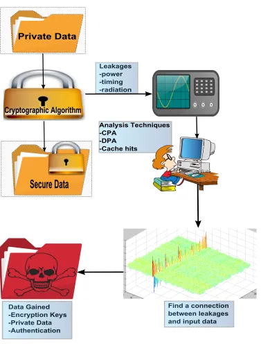
SCAs are a category of attacks, in the cryptographic domain, that take measurable data
from hardware implementations of algorithms and draw correlation to the algorithm’s
in-put. This data can be time [20], power [10], radiation [11] or any phenomenon that is
measurable. Fig. 2.1 shows the flow of mounting a SCA. Private data is given to a
crypto-graphic algorithm that provides some level of security by using mathematical operations.
The attacker collects leakage data using sensors, oscilloscopes, timers, etc. The attacker
then uses various techniques to try and figure out what secret data was processed. These
techniques will be discussed later as they apply to power analysis. SCAs come at the risk
of making secure algorithms insecure with, in some cases, minimal energy and time. SCA
on cryptographic algorithms will be studied as applied to cryptographic hash functions.
2.2
Cryptographic Hash Functions
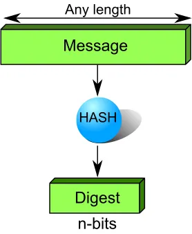
Cryptographic hash functions are a stricter subset of standard hash functions that are similar
to fast data processing functions. A hash function takes a message of any length as an
input and then outputs a set number of bits as seen in Fig. 2.2. Where cryptographic hash
CryptographicEAlgorithm PrivateEData
SecureEData
Leakages -power -timing -radiation
AnalysisETechniques -CPA
-DPA -CacheEhits
DataEGained -EncryptionEKeys -PrivateEData -Authentication
[image:17.612.113.490.118.614.2]FindEaEconnection betweenEleakagesE andEinputEdata
n-bits
HASH
[image:18.612.239.378.87.256.2]Digest
Figure 2.2: Standard hash function operation
output. These properties are [17]:
• Pre-image resistance: givenH(Mi), findMi
• Second pre-image resistance: givenM1findM2such thatH(M1) =H(M2)
• Collision resistance: findM1 andM2 such thatH(M1) = H(M2)
These three properties should be hard to break for an algorithm to be considered a
secure cryptographic hash function. Hard to break is defined by how many combinations
of the output bits, n, need to be tested before one of the conditions above is found.
Pre-image and second pre-Pre-image resistance should be 2n while collision resistance is 2n/2.
With n chosen to be of large enough, brute force searches become unfeasible on current
computing platforms. Cryptographic hash functions are used in many applications such as:
unique message signatures, authenticated encryption, password databases,etc.
2.3
Message Authentication Codes (MACs)
Secure hash functions have many uses when two parties wish to know data has not been
tampered with. This is commonly seen on the internet when a file download has a checksum
listed next to it. The checksum is obtained by running the entire file through a hash function
and generating a message digest. When the user downloads the file, they run the file through
hash function is truly hard to invert, by following the previously defined properties, the user
should be confident the file has not been tampered with.
Another use case for secure hashing is in password databases. If a database stored
usernames linked to passwords, an attacker would only need to steal the database to have
access to all of the user accounts. To mitigate this, secure databases will only store the hash
of a password linked to the usernames. When a user enters his correct password, software
will hash the entered password and compare it to the value in the database. If the hacker
obtains the data in the database, they will only have hashes of the correct password. As
long as the pre-image condition described holds, the attacker would have to brute force
search 2n messages to find a message that hashes to the same value for access to a user
account. This also means that there exists multiple passwords that can be used to log into
a user account, but the property of second pre-image resistance requires finding this to be
hard, i.e. 2n.
The use case that will be explored in this work will be hash functions used for MAC
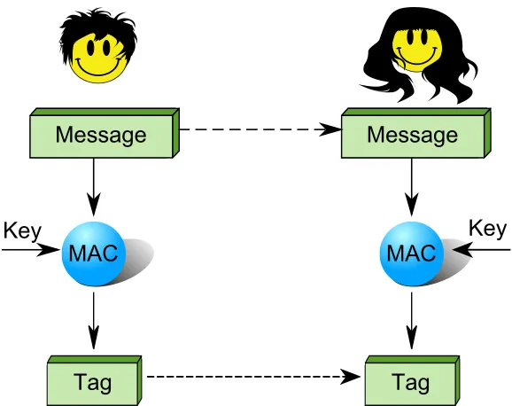
implementations. MACs are used to determine if the message sent from one party came
from that party. Referring to Fig. 2.3, assume the scenario where Bob wants to send Alice
a message, where Bob will be a real user and Alice represents a web server. The first
step involves Bob and Alice both agreeing on a secret key to use by way of public key
cryptography. Public key cryptography is beyond the scope of this work so it will be
assumed that the keys have been properly established and only Bob and Alice know them.
When Bob wants to send a request to Alice, Bob will first send his message through a
hash function to generate a digest/tag. Bob will then send both the message and the tag
to Alice. Upon receipt, Alice will take Bob’s message and put it through the same hash
function to generate a digest/tag. Alice will then compare the generated tag to Bob’s sent
tag. If the tags match Alice can assume that the message came from Bob [17]. In this
case, no encryption is being done. The key is being used as the secret information that will
provide a unique signature that could only be performed by messages originating from Bob
or Alice. This can be further applied to authenticated encryption where SHA-3, the Keccak
Message
Message
Tag
Tag
MAC
MAC
[image:20.612.165.454.86.315.2]Key
Key
Figure 2.3: Standard Message Authentication Code (MAC) Operation
2.4
Merkle-Damgard Vs. Sponge Hash Construction
Hash functions are typically built on algorithms that have a set input and a set output.
Since a hash function is desired to have input of variable size, a step is required to ensure
the input message can be fully processed by the algorithm. There are two dominant theories
for construction: Merkle-Damgard and sponge. Merkle-Damgard uses an idea of chaining
inputs shown in Fig. 2.4. The message is broken intoN blocks based on a multiple of the
defined hash function input and then padded so all inputs to the hash functions are full. For
the first message block, the block is sent to a hash function with some initialization vector.
The output is sent to the next hash function that also takes the next message block. The
multiple inputs to the hash function are XOR’d together to provide a single input to the
hash function. This continues until every message block has been processed in the hash
function. The final hash function output will be the digest.
This works well for solving the variable input problem, but structural weakness in this
construction have been found which reduces the strength of the image, second
HASH HASH HASH Digest
Message 1 Message 2 Message 3 Pad
IV
Figure 2.4: Merkle-Damgard Hash Construction
• Length Extension Attack
• Multi-collision attacks
• Herding attacks
Length extension attacks show up when any Merkle-Damgard based MAC construction
usesH(secretKey||p(message)). The attacker only needs to generate
H(secretKey||p(message)||p(controlledM essage)) (2.1)
The attacker never learns the secret key, and does not have access to the original message.
The hash digest gives the attacker the last state of the hash function that can be used to
generate a new message. The attacker can then compute a new digest from the previous
state with his appended message. This will result in a message and digest that will look to
be valid from another user/server.
Multi-collision and herding attacks follow a similar strategy. The attacker tries to find
a collision on one of the hash outputs. Once this collision is known, the attacker can build
an infinite number of messages that all hash to the same value. This is dangerous if one
thinks about how messages are sent over the internet with standard header information. An
attacker just needs to find a collision at the end of the header and can then generate any
type of message. There would be no way for the other party to distinguish that the original
message has been tampered with. [17]
f
f
f
f
f
rc
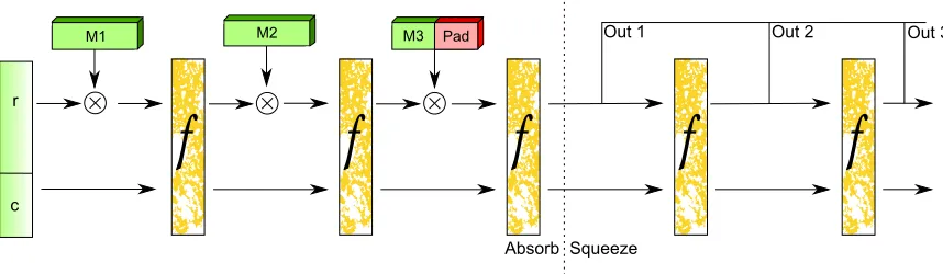
[image:22.612.94.523.92.217.2]Absorb Squeeze
Figure 2.5: Sponge Construction as can be seen in SHA-3
structural problems found in Merkle-Damgard construction [5]. Fig. 2.5 shows the structure
of a sponge function when applied to the Keccak hash permutation. The message is split
into chunks similar to the Merkle-Damgard construction. These chunks are absorbed in the
same manner by XORing the previous state and the current message block and running it
through the hash permutation,f. The difference is the portion of the state,c, that is internal
to the algorithm as is not the case in the Merkle-Damgard approach. It is impossible to
know the final state of the hash construction as only a portion of the state, r, is used as
output. Sponge construction also brings the benefit of variable output as the construction
can continuously be squeezed to generate more output bits. These properties solve the
weaknesses of the Merkle-Damgard construction mentioned above.
This work investigates mitigations of SCA with power analysis on the target
implemen-tation of SHA-3. SHA-3 is a new standard hash function, making it a good target to explore
mitigations on before weaknesses are exploited.
2.5
SHA-3
The National Institute of Standards and Technology (NIST) is a government funded agency
that has the responsibility of establishing and keeping standards in many application
do-mains, which include cryptography. Of their standardized algorithms, they have released a
family of hash functions called secure hash algorithm (SHA). In 2007, NIST held a
and SHA-1 had theoretical breaks. SHA-2 had no known theoretical breaks, but had a
sim-ilar construction to SHA-1. This fueled a desire for a new SHA algorithm. SHA-3 was to
be diversified from the previous algorithms so no theoretical attacks developed for SHA-2
could be easily modified for SHA-3. Keccak was chosen as the winner of the SHA-3
com-petition on Oct 27, 2012. In 2014 NIST published a draft federal information processing
standards (FIPS) publication outlining the standard implementation for SHA-3.
Fig. 2.5 shows the construction of Keccak. Keccak uses a sponge construction where
every hash operation is denoted by anf in the figure. Keccak is then defined by specifying
the values ofrandc. rrefers to the rate of the algorithm and is the speed that messages can
be consumed and digests generated. crefers to the internal capacity and is never propagated
as an output, but controls the level of security of the algorithm. The authors of Keccak
prove that the strength of Keccak is equal to 2c/2 [7]. One Keccak hash permutations is
broken into 12 + 2` rounds where ` is found from 2.2 andw is the size of a word in the
implementation.
w= 2` (2.2)
For simplicity in comparison, the suggested Keccak implementation in FIPS 202 [15]
will be used which has r = 1024, c = 576, and w = 64. This means that the Keccak
permutation will have 24 rounds for any block of input that needs to be absorbed1. The
SCA mitigations discussed in this work are for securing the Keccak permutation to provide
security to SHA-3 and any other algorithm that uses the Keccak permutation as a base.
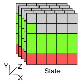
Keccak focuses on manipulation of an internal state at the bit level. The Keccak authors
use a set of terminology when talking about the Keccak permutation that can be seen in
Fig. 2.6. A Keccak state is 5x5xw bits, or5x5x64in this case. The state is filled starting
from(0,0,0)along the z-axis until full, then along the x-axis, and finally the y-axis. Once
r bits have been filled, the remaining state is initialized to ‘0’ to representc. Similar to
chaining algorithms, there must be a padding function that makes sure the input data is a
multiple ofr. The padding function used in SHA-3 is a 10*1 structure where the bits ‘1’,
1
State X
Y Z
Bit Row
Column Lane Plane
Slice
Sheet
Figure 2.6: Keccak state terminology used by the Keccak authors
State X
[image:24.612.270.346.269.349.2]Y Z
Figure 2.7: The filled SHA-3 state for one input vector in MAC configuration
1 tor-1 ‘0’s, and a final ‘1’ bit are appended to the message to ensure it is a multiple ofr.
Fig. 2.7 shows how the state will be filled for experiments in this work. The bottom plane
will contain a 320-bit key, followed by two more planes (640-bit) and one lane (64-bit) of
random input. The key will be, in hex format: {00,01,02,03,...,39}.
The Keccak permutation then can be describe in 6 distinct operations: State XOR,
theta(θ),rho(ρ),pi(π),chi(χ), andiota(ι).
2.5.1 State XOR
The State XOR involves filling a Keccak state and then performing the bit-wise XOR
op-eration between the current state and the previous state. In the case of the first state, the
previous state is a Keccak state with all ‘0’ bit entries. This provides the absorption
prop-erty of the sponge construction. Power analysis at this state is not a primary target as the
initial state and the input are known. This would be a good attack point if a random
initial-ization was used for the state, instead of the FIPS recommended all zeros state, to identify
2.5.2 Theta (θ)
θ provides column diffusion by calculating each column’s parity and using an XOR
func-tion to combine two neighbor columns. This is defined by:
S[x][y][z] =s[x][y][z]⊕(⊕4
i=0(s[x−1][i][z])⊕(⊕ 4
i=0(s[x+ 1][i][z−1]) (2.3)
To reduce hardware complexity of having an 11-bit XOR operation for every output bit,
θ is typically implemented in two phases: the θ plane creation and theθout phases. Theθ
plane creation follows:
θplane(x, z) = ⊕4y=0(s[x][y][z])
x∈ {0,1, ...,4}, z∈ {0,1, ...,63}
(2.4)
Theθplane is created with 5-bit XOR operations. Theθout phase can be implemented
with 3-bit XOR operations as follows:
θout(x, y, z) =s[x][y][z]⊕θplane(s[x−1][i][z])
⊕θplane(s[x+ 1][i][z−1])
x, y ∈ {0,1, ...,4}, z ∈ {0,1, ...,63}
(2.5)
Fig. 2.8 show a visual representation of the state operation. The output at a single bit in
the state is the current bit and the 10 bits of two neighboring columns. In hardware, this is
typically done in two stages. 320 5-bit XORs convert the columns into a 5x64 plane. 1600
3-bit XORs take an initial bit and 2-bits from the θplane to create the output ofθ. This is
a good SCA attack point as there is a mixing of known and unknown bits in the creation of
theθplane andθout.
2.5.3 Rho (ρ)
ρ provides inter-slice diffusion inside the state. This is done by rotating the lanes by an
θ
[image:26.612.222.399.87.293.2]Figure 2.8:θpermutation of Keccak state.
Figure 2.9:ρpermutation of Keccak state [7]
operation is:
S[x][y][z] =s[x][y][z−(t+ 1)(t+ 2)/2],
wheret=
(0 1 2 3)
t
(1 0) = (
x
y) 0≤t <24
−1 x=y = 0
(2.6)
Fig. 2.9 shows a visual representation of theρpermutation. Table 2.1 shows the offsets
that are used for each of the lane rotations that follow 2.6. The permutation in hardware
Table 2.1: ρoffsets
x=3 x=4 x=0 x=1 x=2 y=2 153 231 3 10 171 y=1 55 276 36 300 6 y=0 28 91 0 1 190 y=4 120 78 210 66 253 y=3 21 136 105 45 15
2.5.4 Pi (π)
π provides long term diffusion by permuting the lanes to different locations in the state. π
is mathematically defined as a multiplication of the current state by a matrix in GF(5) as
follows:
S[x][y] =s[x][y]∗(0 1 2 3)
|
(2.7)
The entire lane, values along z-axis, moves to the new (x, y) coordinate. Also, the
permutation defines the center state as (x, y) = (0,0), where as during state filling, the
bottom left bit has (x = y = 0). Fig. 2.10 shows a visual representation of π. The
permutation is broken down into 6 subfigures where the movement happens about the center
(0,0)point. Sinceπis just a remapping of bits, this is a bad SCA target for the same reason
as mentioned forρ.
2.5.5 Chi (χ)
χprovides the only non-linear function of Keccak, important so Keccak is not vulnerable
to linear cryptographic analysis. χcan be thought of as 5-bit,5wparallel S-boxes operating
on the rows of the Keccak state. It is mathematically defined as:
S[x, y] =s[x, y]⊕(N OT(s[x+ 1]), y)s[x+ 2, y]) (2.8)
Fig. 2.11 shows a visual representation of theχpermutation involving one XOR, one
AND, and one NOT gate per state bit. This non-linear operation was chosen by the authors
Figure 2.10: πpermutation of Keccak state [7]
Table 2.2:ιround constants
RC[ 0] 0x0000000000000001 RC[12] 0x000000008000808B RC[ 1] 0x0000000000008082 RC[13] 0x800000000000008B RC[ 2] 0x800000000000808A RC[14] 0x8000000000008089 RC[ 3] 0x8000000080008000 RC[15] 0x8000000000008003 RC[ 4] 0x000000000000808B RC[16] 0x8000000000008002 RC[ 5] 0x0000000080000001 RC[17] 0x8000000000000080 RC[ 6] 0x8000000080008081 RC[18] 0x000000000000800A RC[ 7] 0x8000000000008009 RC[19] 0x800000008000000A RC[ 8] 0x000000000000008A RC[20] 0x8000000080008081 RC[ 9] 0x0000000000000088 RC[21] 0x8000000000008080 RC[10] 0x0000000080008009 RC[22] 0x0000000080000001 RC[11] 0x000000008000000A RC[23] 0x8000000080008008
be thought of as a 5-bit S-Box, the typical attack point in AES. [27] shows when keys get
larger than one plane,χis a required attack point for finding the full key. Also, they show
using a larger key gives the best security, with keys that are multiples ofr being the most
effective. In this work, χwill not be looked at as a SCA analysis point as it is not needed
for keys that reside only in the first Keccak plane. If mitigations work for keys residing in
a single plane, they are inherently valid for the more complicated cases.
2.5.6 Iota (ι)
ι is the last permutation of the Keccak hash function. A constant value is XOR’d with the
first lane(0,0). This constant value is different for every round making each Keccak round
different. The round constant comes from a 64-bit linear feedback shift register (LFSR).
This mitigates the chance of the Keccak state entering a cycle. A cycle, in the context of a
cryptographic algorithm, is when a previous round output is generated by a future round.
The consequence is that the rounds in the middle have no impact on the algorithm, greatly
reducing security. χ and θ ensure the value from ι is mixed into the state the following
round. Table 2.2 shows the round constants for the 24 rounds of Keccak. ιhas 64 unknown
values and 64 known values. This could be used as a SCA analysis point, but only for the
first 64-bits of the key. If the key is longer then 64-bits, which is recommended, another
Weight W
n
Input Xn
Output Y
Neuron
(integrator)
Figure 2.12: A simple neron model
For SCA mitigations, many groups have looked at using different digital CMOS
strate-gies to mitigate attacks with no clear umbrella solution. The neuromorphic computing
paradigm implements logic much different than traditional AND, OR, etc gates by using
inspiration and abstractions from the human brain. Analog circuits, that are more
suscepti-ble to noise, could provide enough randomness to help decorrelate leakage data in a circuit
to the input being processed.
2.6
Neuromorphic Computing
Neuromorphic computing is a field that has groups who wish to mimic how the brain
oper-ates or build systems that take inspiration from abstractions of the brain. Our current Von
Neumann computing architectures are very efficient and reliable when it comes to typical
number crunching; however, the hard to solve problems, that make up the computer
vi-sion and machine intelligence domains, are not made easier from number crunching. Even
though a computer can compute many Fourier transforms a second, a task that we could
never hope to achieve, it can be near impossible for a computer to distinguish a cat from a
dog [18].
This work does not attempt to implement neuromorphic computing components in
to implement neuromorphic computing components to take advantage of some of their
in-herent properties. The brain with its approximate 20 billion neurons has single neurons
connected to 10,000 other neurons. These connections are called synapses, and it is
be-lieved that the connections, or lack of connections, is the result of learning and forgetting.
Signals propagate through the brain when these neurons are stimulated from the amount
of input they receive. The important properties from the brain for this implementation are
its low power, approximately 20 W for the entire brain, and its stochastic nature of
oper-ations, thanks to the synaptic connections. Fig. 2.12 shows the model that will be used,
a single neuron with 5 synaptic connections. An activation function, described in section
3.3, will determine when the neuron should be active. Equation 2.9 describes this neuron
model whereX is the input,W is the corresponding weight andY is the output after
ap-plying some activation function. Synaptic weights will be used to mimic the concept of
plasticity in the brain where connections to the neuron can be strengthened or weakened
depending on what a desired output should be2. This can be implemented in memory units
in digital design, but is not easily scalable if network size becomes too large. Memristor
devices, in the analog domain, can be used to provide for many adjustable states in simple
two-terminal devices.
Y =activation(
5 X
n=1
Xn∗Wn) (2.9)
2.7
Memristor Devices
Memristor devices link charge and magnetic flux [28]. They are thin film, two-terminal,
passive circuit devices that are known for their pinched hysteresis loop shown in Fig. 2.13.
When the memristance of the device is held constant, it acts as a simple resistor following
the relation:
I = V
M (2.10)
2For more detailed information, [16] goes more in-depth about computational neuromorphic computing as only a few
Figure 2.13: I-V characteristice of the piecewise linear memristor model [24]
The output strength is configured by adjusting the propertyM allowing for the concept
of a synaptic weight to be realized with one device. This device allows for highly scalable
architectures due to the simple two-terminal nature of the memristor. For digital design,
this would require a memory unit for every synaptic weight bit of precision. The calculation
of the synaptic weight and input is done by the differing amount of current that can flow
through the memristor based on its configured resistance. The summation step, in the
analog domain, is done by a shared memristor node. This leads to a massive resource
savings as flip-flops to store weights, multipliers to calculate synapse responses, and adders
Chapter 3
Supporting Work
3.1
SCA with Power Analysis
SCA can consist of analyzing power consumption [10], electromagnetic radiation [11],
timing information [20], cache hits/misses,etc. For this work, only power analysis will be
explored as it relates to simple power analysis (SPA), differential power analysis (DPA), and
correlation power analysis (CPA). Power analysis is made possible because of the transistor
properties in CMOS design. When a transistor transitions to a logic ‘0’ or to a logic ‘1’,
it consumes power. The power has been shown to be consistent over multiple similar
operations by an experiment done by Paul Kocher [10]. Fig. 3.1 shows the distribution
between of power consumed for an AES S-box operation. The least significant bit (LSB)
of the S-box output, an 8-bit value, was targeted. The power consumed for 16,000 traces
was separated into two bins based on if the LSB was ‘1’ or if it was ‘0’. The figure shows
that the mean distribution when the LSB was ‘1’ is different than that of when it was ‘0’.
Power analysis tries to find patterns between this characteristic power consumption and the
input being processed of a specific cryptographic algorithm.
3.1.1 Simple Power Analysis (SPA)
SPA attempts to decipher what is going on inside a hardware implementation based on
how much power is consumed in a circuit from a single waveform. Fig 3.2 shows a power
trace from an implementation of Rivest-Shamir-Adleman (RSA), one of the first public key
encryption algorithms. In [10], it is shown that by looking for the peaks at each clock edge,
the RSA key can be obtained by noting that a large peak corresponds to a ‘1’ and a small
Figure 3.1: Distribution of power over 16000 traces in an AES hardware implementation [10]. The distribution on the left is when the LSB was ‘0’ while the distribution in the right with the the LSB was ‘1’.
in RSA that are dependent on the current bit (‘1’ has more operations than ‘0’). This is a
dangerous problem as a secret key can be found by human inspection in a matter of seconds
with no required knowledge of the input or output to the system.
SPA can show features in a power trace to indicate when certain operations are
hap-pening inside a cryptographic system and how long they are taking. Once features can be
determined in power traces, an attacker can use these features to help extract key
informa-tion; however, SPA is generally not used to attack current cryptographic implementations
as it is very easy to counter. A small amount of noise in the system may be enough to mask
the signal to where it is not easily deciphered from inspection. Also, this noise can make
attack automation hard when trying to determine if a certain feature is present or not. With
a single trace, it is hard to reduce noise, which is where DPA comes in.
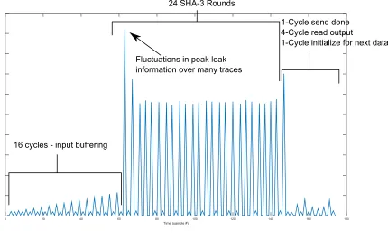
Fig. 3.3 shows a single SHA-3 power trace. From this power trace, it is possible to see
the cycles that are used to load the data, the cycles are used for the permutation rounds,
and the cycles are used to generate output. This can facilitate reducing the search space of
a waveform for an attack; yet, the data of interest to determine the secret key resides in the
variations of the waveform peaks. It can require thousands of traces and statistical analysis
Figure 3.2: Power trace from an implementation of RSA where the secret key can be deduced from a single trace. Red represents the parts of the waveform that leak the bit is ‘1’, green represents the parts that leak the bit is ‘0’ [10]
Time3ksample3dv
0 20 40 60 80 100 120 140 160 180
163cycles3-3input3buffering
243SHA-33Rounds
1-Cycle3send3done 4-Cycle3read3output
1-Cycle3initialize3for3next3data
Fluctuations3in3peak3leak information3over3many3traces
DPA was developed in [10] to provide a more robust way to find secret keys that is resistant
to noise and can easily be automated. The following shows the mathematical formula for a
DPA attack:
∆Dj[t] =
Pm
i=1S(Mi, Kj)Pi[t]
Pm
i=1S(Mi, Kj) −
Pm
i=1(1−S(Mi, Kj))Pi[t]
Pm
i=1(1−S(Mi, Kj))
(3.1)
Fig 3.4 shows a visual model for the attack strategy using 3.1. Many input messagesM,
broken into individual messagesMi, are created and given to a cryptographic
implementa-tion. Power tracesP, broken into individual power tracesPi, for each input vector are then
collected. The secret key is broken up in sections depending specifically on what makes
sense for the algorithm under attack; generally, it is the size of the nonlinear permutation to
make calculations easier. For this example, assume the key,K, is 128-bit and is broken into
8-bit guesses,Kj. Each key section has 256 key guesses that range from 0 to 255. For each
key guess, the attack will attempt to find the outputIij, whereIij =S(Mi, Kj)andS(. . .)
is a selection function that determines if a bit under attack is a ‘1’ or ‘0’. Once the attacker
has this, they can target one bit ofIij and divide all power traces into two bins based on if
the target bit is a ‘1’ or a ‘0’. From Fig 3.1, if the current guess is right, it should correctly
split the power traces into groups that represent the power consumption in the circuit. If it is
an incorrect guess, it should split the power traces randomly. Once the attacker has a bin for
output ‘0’ and ‘1’, they average the bins and then take the difference of them. Because of
the previous found result that the power consumption differs depending on the value of the
bits, the correct differential trace should be the one that has the largest peak. Differential
traces from wrong guesses should approach zeros with enough traces in the attack. This is
because the sample mean of a random distribution, over enough samples, should converge
to the distribution mean; thus making the difference of two different random samples of
one distribution head toward zero. Fig. 3.5 shows a sample of power traces from an attack
Selection Function
Messagei
Key Guessj
-or-Differential TracejPower Tracei
Bin0 Bin1
[image:37.612.205.418.104.411.2]-Figure 3.4: Differntial power analysis attack model
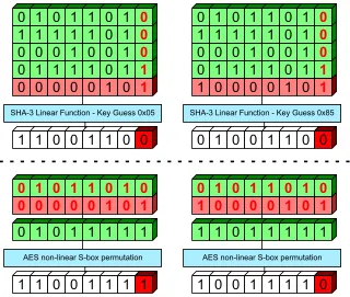
SHA-3 Linear Function - Key Guess 0x05 SHA-3 Linear Function - Key Guess 0x85
AES non-linear S-box permutation
0 0 0 0 0 1 0 1
0 1 0 1 1 0 1 0
1 1 0 0 1 1 1 1
0 1 0 1 1 1 1 1
AES non-linear S-box permutation
0 0 0 0 0 1 0
1
0 1 1 1 1 0 1
1
0 0 0 1 0 0 1
0
1 0 0 0 0 1 0
1
0 1 1 1 1 0 1
1
0 0 0 1 0 0 1
0
1 1 0 0 1 1 0 0
[image:38.612.148.468.89.360.2]1 0 0 1 1 1 1 0
1 1 0 1 1 1 1 1
1 0 0 0 0 1 0 1
0 1 0 1 1 0 1 0
0 1 0 0 1 1 0 0
Figure 3.6: An example of a non-linear’s and linear function’s impact on output bits for key guesses of 0x05 and 0x85. The top examples are for SHA-3 (linear) while the bottom examples are for AES (non-linear). Light red indicates the portion of the operation that is controlled by the attacker for generating outputs to the selection function (key guess). The dark red numbers represent the bits that can affect the dark red block, the target bit in DPA.
DPA is insensitive to noise because of differential traces. The more traces used, the
more likely any random noise will be removed during the differential subtraction step.
This attack works well when it is used on non-linear portions of a cryptographic algorithm
because small changes in the input of the non-linear portions should have a large effect on
the output. For algorithms where the best attack points are linear, problems with the DPA
method can be seen.
An example showing a comparison of DPA between linear and non-linear functions can
be seen in Fig. 3.6. This shows the linear SHA-3 operation of theθ plane creation versus
the non-linear S-box function of AES, which has an XORing of a round key before the
function. Both operations use an XOR function of some known data and some secret key
data. A key of 0x05 and 0x85 are shown together to see the different effects on the output
guess can only impact the same bit in the output. In the AES case, changing any bit in the
input to the non-linear function can have an impact on any output bit. This is important as
DPA targets certain bits of the output. If only the LSB is considered, the impact of the the
plain text bits from the MSB to LSB+1 are thrown away when figuring out the bin to put
the waveform in for the SHA-3 case. This throws out the differing power of the transistors
in the circuit that do not directly effect the target bit, most bits in the design. As such, the
non-linear function can be seen as a function that is providing some amount of information
about all bits that enter it, while linear functions need some other methodology to get this
information.
3.1.3 Correlation Power Analysis (CPA)
CPA was first described in [8]. It is based off the Pearson correlation coefficient that
de-termines the relationship between how two random variables change. CPA works because
it has been shown that there is a strong correlation between the transistors that have
transi-tioned and power consumed than just the current state of the transistors (as in DPA). When
the number of transistors set is used, this is called hamming weight. When the number
of transistors that have changed value is used, this is called hamming distance. Hamming
weight and hamming distance are referred to as power models of CMOS circuits, and allow
for characterization of a circuit to be reduced to correlation between its power consumed
and one of these models. CPA tries to find the correlation between power consumed and
either the hamming weight or hamming distance of the input and output of the algorithm.
The lower the magnitude of the correlation coefficient, the less likely a key guess is the
correct key.
The Pearson correlation coefficient is shown in 3.2. The Pearson correlation coefficient
is the covariance of the data, power traces and hamming distances/weights, divided by the
variance of the two distributions.
ρ= cov(x, y)
σxσy
(3.2)
For linear functions, CPA solves the problem of DPA involving a lack of correlation
Since this work will focus primarily on mitigations to current implementations of CMOS
designs in the cryptographic context, it is important to discuss the leading proposed
solu-tions. The majority of proposed mitigations use the same CMOS digital design principles
to reduce power leakages that are at the root cause of the problem. A neuromorphic design
in the analog design domain will be proposed as a possible competing solution.
3.2
Current Mitigating Designs
3.2.1 Dual-rail with Precharge Logic
Dual rail with pre-charge logic is a family of mitigation designs that split transistor
opera-tion into a pre-charge and evaluaopera-tion phase with the addiopera-tional use of complementary logic.
The pre-charge phase is meant to set the circuit to a known electrical state before any bit
transitions happen, eliminating the use of the hamming distance power model. The
com-plementary logic is meant to mask the power of the number of bits set in the cryptographic
algorithm, eliminating the use of the hamming weight power model. The evaluation phase
is the normal phase where a bit becomes a logic ‘1’ or logic ‘0’.
Wave Dynamic Differential Logic (WDDL) attempts to hide power consumption by
replicating the inverse of the circuit so that every bit transition from ‘1’ to ‘0’, there also
exists a ‘0’ to ‘1’. Fig. 3.7 shows an example of a WDDL AND gate. This was tested on
an FPGA [9] and found effective against DPA. The authors suspected that more sensitive
measurement equipment might be able to mount a successful SCA. Shortly after, a new
attack that focuses on a condition called the Early Evaluation (EE) effect was developed
that exploits a condition where two inputs to a logic gate arrive at different times [26].
Assume the case where the values of A and B are set to ‘1’ in Fig. 3.7. Initially, all inputs
to the two gates are ‘0’, pre-charge, setting the output of both gates to logic ‘0’. During the
evaluation phase, if A and B arrive at some 4t time different from each other andA¯and
¯
B arrive at the same time, the OR gate would transition to its correct state of logic ‘0’4t
A
B
out
WDDL AND
A
[image:41.612.236.384.86.246.2]B
out
Figure 3.7: Wave Dynamic Differential Logic implementation of an AND gate. Not shown is the pre-charge circuitry that ensuresA,B,A¯andB¯ are initialy logic ‘0’ before the evaluation phase.
a simple problem to solve as it would require exact capacitance matching in VLSI layout.
Masked Dual-rail Pre-charge Logic (MDPL) attempts to avoid the need for perfect
bal-ancing of wires inside the design by masking every value and pre-charging cells [19]. This
comes at the cost of increased power consumption and area overhead as much as a factor
of 4. The design was shown to run slower than WDDL; yet, it does not have the
notice-able attack vulnerabilities of WDDL and does not require capacitance balanced wires. This
makes for an easier implementation, but at the cost of higher power consumption and much
larger area.
Secure Triple Track Logic (STTL) solves the problem of EE by adding a
synchroniza-tion signal to the pre-charge/evaluasynchroniza-tion signal to prevent evaluasynchroniza-tions until all signals are
valid [23]. It requires a synchronization signal that is slower than the dual-rail logic delay
providing a design that runs slower for cases that would not normally need synchronization.
The benefit is that this logic style can be considered completely dual-rail.
Balanced Cell-based Differential Logic (BCDL) is the final design that will be discussed
in this family of mitigations that improves on STTL by using a fast global synchronizing
signal [14]. This design is still slower than MDL and WDDL but faster than STTL.
There are also many variations on the WDDL implementation that will not be discussed
here. They can be seen to improve on the basic WDDL flaws, but not at a level that would
the cryptographic operation being performed. Code is analyzed to determine blocks that
contain cryptographic calculations and then random code is inserted into these blocks. This
was shown to be effective against DPA but at the cost of 30% longer run times and 27%
higher power consumption. Also, these designs run on processors that lose the benefit of
fast gate-level algorithm designs.
All the presented mitigation designs make minor modifications to the current design
paradigm of digital CMOS logic with varied success. It stands to reason that stepping out
of the digital CMOS design context, that has the inherent properties allowing information
leakage, may help to find circuits that have strengths against power analysis.
3.3
Neural Logic Block (NLB)
The architecture that will be explored in this work is the NLB. Specifically, the NLB of
focus is the Multi-threshold NLB (MTNLB) proposed in [24]. An NLB is a component
that uses the computational neuromorphic computing principles discussed in section 2.6.
The NLB is a single layer component capable of learning any basic logic function: AND,
NOT, OR, XOR, XNOR, NAND, NOR, and any n input functions. What is important to
note, XOR/XNOR are examples of operations that are not linearly separable. An example
of this linear separable concept is shown in Fig. 3.8 with a 2-input AND gate compared
to a 2-input XOR gate. The AND gate has one decision boundary, when both inputs are
high. The XOR gate was two decision boundaries: when both inputs are high and when
both inputs are low. The AND gate could be represented using a single layer neuron that
learns the function of the hyperplane; however, the XOR gate would need two neurons that
learned the described hyperplanes and a second level that combined them to a single result.
Since the NLB does not use simple monotonic activation functions, it can implement any
n input function as long as the activation function hasn+ 1boundaries. This component
1
1
0
1
1
0
XX X
AND
XOR
Figure 3.8: Seperability of AND and XOR logic functions. The green circle with an X represents when the output is desired to be a one while the red circle represents when the output should be zero.
used in FPGAs.
The non-monotonic activation function is shown in Fig. 3.9 with the left plots
represent-ing trainrepresent-ing without a bias signal and the right plots with a bias signal. AND and OR gates
only have one decision boundary, where all inputs are logic ‘1’ for AND or when one input
is logic ‘1’ for OR. For the XOR function, ann-bit XOR function requiresn+ 1boundaries
as the output toggles based on the number of inputs that are active. The same is true for
NAND, NOR and XNOR except now it is desirable for the output to have a ‘1’ when all
inputs are ‘0’. For a generic activation, the bottom plots show how scaling the values of the
thresholds can let one activation function map to many different logic functions.
Because of the random weight initialization with training, the amount of power
con-sumed for any n-inputs will be inherently different, as there are multiple weight
combi-nations that could generate the same desired output [24]. The goal is to mask the power
dissipation by adaptive use of the MTNLB. The stochastic nature of the synapse weights
in the MTNLB network, with bipolar weights, will provide variability in the power traces;
moreover, there is a significant reduction in the power consumption with the MTNLB
com-pared to standard lookup table or CLB logic, as shown in Fig. 3.10. This is important as
smaller power fluctuations in a power trace will cause more traces to form correlations.
Lastly, it is also shown that the MTNLB, when implemented in analog-digital mixed signal
Figure 3.9: Plot of activation functions for AND, OR, XOR, NAND, NOR and XNOR functions. The top plots are the desired activation for each labeled gate. The bottom plots shown how the activation functions can be realized with one standard activation function. No bias is shown on the left and using a bias is shown on the right [24].
in an FPGA. This means that MTNLBs could be used to replace, or compliment, LUTs
in an FPGA to provide SCA mitigation to any implemented cryptographic algorithm. The
characteristics that are hoped to be exploited in the MTNLB to produce a SCA resistant
circuit are:
• Inherent device variability of the memristor (process variations)
• Ultra low power design (several orders of magnitude less)
• Stochastic power consumption based on the trained values of memristor (unique to
each NLB)
• Less required resources (Less resources used to implement MTNLB compared to
Chapter 4
Hardware Circuits
The circuits in this work are split into two groups: digital and analog. The digital section
circuits implement the full SHA-3 algorithm, while the analog circuits only implement the
θ plane due to the length of simulation. To provide accurate comparisons between the
analog circuits that have onlyθimplemented to the full digital implementations, all circuits
discussed in section 4.1 will have another circuit with only θ implemented. The digitalθ
only circuits will not be discussed as they are a subcircuit of the presented circuits.
4.1
Digital Implementations
4.1.1 High-Speed Core - Base Circuit
For analysis of the SHA-3 algorithm, the SHA-3 high-speed core implementation provided
by the SHA-3 authors was used [6]. This HDL model was modified when adding
mitiga-tions to provide a base for comparison of mitigamitiga-tions to no mitigation. Fig. 4.1 shows the
block level diagram of the high-speed core. Starting from the left, the input into a round
is either the previous state, in the case of squeezing, or the previous state XOR’d with a
new block of input, in the case of absorbing. The block diagram shows a 5x5x5 cube for
simplicity, but the actual state in all circuits will by 5x5x64. From here, the columns of the
1600-bit state are XOR’d to generate a 5x64 plane that is called theθ plane. To generate
the resultingθoutput, the bit at(x, y, z)is XOR’d with two-bits in theθplane as discussed
in section 2.5.2 to obtain θout(x, y, z). The next phases ofρandπare remappings. Theχ
operation takes each input bit and applies a non-linear function comprised of 3 logic gates,
AND, XOR, and NOT per bit. The final operation is a 64-bit XOR on the first lane of the
π ρ
θ θ Plane
χ
Iota Round Input
Round Counter == 0
SHA-3 Core
Figure 4.1: Block diagram of the basic SHA-3 high-speed core implementation. The state is repre-sented as a5x5x5cube where as the actual implementation is5x5x64. The blue colored gates and state bits show an example of creating oneθ(x, z)plane bit and also theιstep. The red gates and state bit show an example of how oneθout(x, y, z)bit is created.
4.1.2 Mitigation One - Dual Core Design
The first circuit for SCA mitigation testing was to use two simultaneously instantiated
SHA-3 high-speed cores. The first core would perform the SHA-3 hash algorithm while
the second core would compute the SHA-3 hash with inverted input data. This design is
inspired from the dual-rail logic family where every ‘0’ to ‘1’ bit transition has a
com-plementary ‘1’ to ‘0’ transition. Since the θ plane creation uses a linear function, XOR,
dual-rail logic can be implemented by using the inverse input data. This is not full dual-rail
logic as this does not hold for the χ permutation. Since the attack is happening on the
θ plane, the methodology is valid. Fig. 4.2 shows the block diagram for this mitigation
circuit. Two SHA-3 cores are instantiated and one is fed the normal input data while the
second receives the inverse data by using 1600 NOT gates, one for each bit.
4.1.3 Mitigation Two -θPlane Masking
For a more compact digital implementation, mitigation two uses the inverse operation on
π
ρ
θ
θ
Plane
χ
ι
SHA-3 Core
π
ρ
θ
θ Plane
χ
ι
Round Input
Round Counter == 0
[image:48.612.95.524.193.513.2]SHA-3 Core
Figure 4.2: Block diagram of the SHA-3 dual-core mitigation. The state is represented as a5x5x5
π ρ
θ θ Plane
χ
ι Round Input
Round Counter == 0
SHA-3 Core
Figure 4.3: Block diagram of the SHA-3 XNOR θplane mitigation. The state is represented as a
5x5x5 cube where as the actual implementation is5x5x64. The blue colored gates and state bits show an example of creating oneθ(x, z)plane bit and also theιstep. The red gates and state bit show an example of how oneθout(x, y, z)bit is created.
set of XNOR gates to calculate the inverse θ plane. This saves on1600∗3gates that are
used in theχpermutation and the one 64-bit gate used duringι. Fig. 4.3 shows the block
diagram of this circuit.
4.1.4 Mitigation Three - NLBθPlane Masking
The third mitigation uses the concepts of NLBs discussed in section 3.3. The
implemen-tation of MTNLBs presented in previous work has been an analog implemenimplemen-tation. This
work will implement both an analog and digital MTNLB circuit to compare mitigation in
different design domains. Power analysis success results from characteristic power
con-sumption seen in CMOS circuits; thus, implementing the MTNLB in digital logic can
show the possibility of decorrelating power consumption from input data while still using
full digital CMOS logic.
Fig. 4.4 shows the high level block diagram of this mitigation. The 5-bit XOR gates in
the θ plane creation step are replaced with 5-bit MTNLBs. Fig. 4.5 shows the RTL level
π ρ
θ χ
ι
Round Input
Round Counter == 0
NLB 5
NLB 5
NLB 5 5
Figure 4.4: Block diagram of the SHA-3 NLB θ plane mitigation. The state is represented as a
5x5x5 cube where as the actual implementation is5x5x64. The blue colored gates and state bits show an example of creating oneθ(x, z)plane bit and also theιstep. The red gates and state bit show an example of how oneθout(x, y, z)bit is created.
input and the MTNLB. These weights are trained outside of this RTL model using Matlab.
This was done as the power consumption of the training phase is not as important as the
power consumed during the cryptographic hash computation. The weights are represented
using fixed point notation(Qm, Qn)whereQm is the number of integer bits andQn is the
number of fractional bits. The(Qm, Qn) used in this implementation is(3,4)for a total of
8-bits.
Normally the synaptic response between the input and the neuron is found by
multi-plying the synaptic weight with the corresponding input. This works well in software, but
in hardware this would require a (Qm, Qn)x(Qm, Qn)multiplier for every input. In this
design, there is a need for 320 5-bit MTNLBs resulting in 320∗ 5 multiplier units. To
simplify this, an 8-bit, 2-1 MUX is used for every synaptic input and uses the XOR input,
either ‘0’ or ‘1’, as its select line. If the input is low, it will pass on the value of ‘0’, while if
the input is high, it will pass on the value of the synaptic weight. The outputs of these 8-bit,
2-1 MUXs will be summed using an adder tree of(Qm, Qn)bit adders. For the neuron
ac-tivation function, the non-linear function described in section 3.3 will be used. This will be
0 0 0 0 0 weight81 weight82 weight83 weight84 weight85 Inputs X
NLB
Synaptic8Sum Activation8Func X 43 X 85 X 128 X 170 X 213 sel1 sel2 sel3 sel4 sel5 sel6Figure 4.5: RTL Diagram of MTNLB. The left shows how synaptic summation is implemented while the right shows how the MTNLB activation function is implemented.
synaptic sum falls into. In this case, there are 256 possible values as the fixed-point number
is 8-bit. The 256 values are split into 6 sections fulfilling the n+ 1 decision boundaries
requirement to ensure a possible solution. The final output of the MTNLB will be either
‘0’ or ‘1’ dependent on an even boundary being active (active low in this implementation).
This is equivalent to the activation function outlined in the MTNLB description.
4.2
Analog Implementations
Digital circuits are ineffective at implementing some of the basic features found in
neuro-morphic design, such as addition, weight storage and synaptic response calculations. The
analog implementations were only implemented for the θ permutation due to simulation
time. These circuit will be compared to the corresponding digital θ only circuit for fair
comparisons.
4.2.1 Mitigation Four - NLBθPlane Masking - default
The MTNLB can be broken down into three main components, the global trainer, the
range-select/local trainer and the activation function as shown in Fig. 4.6.
Fig. 4.7a shows the range-select component. It takes a voltage input and performs the
Global Trainer
Range Select Trainer Trainer Trainer Trainer Trainer Activation FunctionXi-n Xi-n
[image:52.612.98.525.369.615.2]seli-m m+,m-,ClkSel Y Y Yexp Yexp
Figure 4.6: Block level diagram of the analog MTNLB. For one MTNLB there is a single global trainer,nlocal trainings,nmemristors, one range select component and one activation function.
W2 Wn X1 X2 Xn W1 sel1 sel2 selm-1 selm iref1 iref2 iref(m-1) (a) Xi Xi m+ Wi 'Z' vi Xi m-ClkSel ClkSel (b) x1 x2 xn sel2 sel4 selm Yexp Yexp Ycomp Y D Q (c) D Q Q ClkSel m+ m-D Q Q SEL NEG R/W Yexp Y Clk (d)
Figure 4.7: (a) shows the range select component. It consists ofnlocal trainers (red),nmemristors,
n comparators (green) andlog2(n) NAND gates(blue). (b) shows the local trainer circuit. ’Z’ is
The currents are summed by a shared node instead of the need for adders as in the digital
implementation. This summed current is sent toncomparators where the number of
com-parators is equal to the number of inputs of the MTNLB. The comcom-parators find the range,
m, that the summed current falls into by having one of the active-low select lines be active.
By design, only oneSelmsignal is active at a time.
Inside the range-select block aren local trainers whose responsibility is adjusting
in-dividual synapse weights, memristors, based on control signals from the global trainer.
Fig. 4.7b shows the circuit diagram for the local trainer. The signalsClkSel,m+andm−
come from the global trainer. WhenClkSel is high, the values ofm+andm−are valid
for training. If the input, Xi, is low, the value of ‘0’ is passed through the MUX and the
weight of the memristor is unchanged. If the value of Xi is high, the values of m+ and
m−are applied to the memristor to change its internal state. m+ andm− are set by the
global trainer to correctly increment or decrement the memristor state. When ClkSel is
low, there is no training to be done, and the voltage on the input of the memristor is Xi
while the output is summed together with the rest of the memristors.
The activation function takes, as inputs, the active-low select lines from the range select
block, seli and the inputs to the MTNLB,Xi. Fig. 4.7c shows the circuit diagram for the
activation function. The activation function is a generic function where the desired function
is configured by changing the reference currents in the range-select block. To get the
non-monoton
![Figure 2.9: ρ permutation of Keccak state [7]](https://thumb-us.123doks.com/thumbv2/123dok_us/41821.3572/26.612.222.399.87.293/figure-r-permutation-of-keccak-state.webp)
![Figure 2.10: π permutation of Keccak state [7]](https://thumb-us.123doks.com/thumbv2/123dok_us/41821.3572/28.612.223.397.398.652/figure-p-permutation-of-keccak-state.webp)
![Figure 3.5: Differntial power analysis on AES key showing guess 1,2,3,4,5, where guess 3 is thecorrect key byte [10]](https://thumb-us.123doks.com/thumbv2/123dok_us/41821.3572/37.612.205.418.104.411/figure-differntial-power-analysis-showing-guess-guess-thecorrect.webp)