A 64-Point Fourier Transform Chip for High-Speed
Wireless LAN Application Using OFDM
Koushik Maharatna, Eckhard Grass, and Ulrich Jagdhold
Abstract—In this paper, we present a novel fixed-point 16-bit word-width 64-point FFT/IFFT processor developed primarily for the application in an OFDM-based IEEE 802.11a wireless LAN baseband processor. The 64-point FFT is realized by de-composing it into a two-dimensional structure of 8-point FFTs. This approach reduces the number of required complex multi-plications compared to the conventional radix-2 64-point FFT algorithm. The complex multiplication operations are realized using shift-and-add operations. Thus, the processor does not use a two-input digital multiplier. It also does not need any RAM or ROM for internal storage of coefficients. The proposed 64-point FFT/IFFT processor has been fabricated and tested successfully using our in-house 0.25- m BiCMOS technology. The core area of this chip is 6.8 mm2. The average dynamic power consumption is 41 mW at 20 MHz operating frequency and 1.8 V supply voltage. The processor completes one parallel-to-parallel (i.e., when all input data are available in parallel and all output data are generated in parallel) 64-point FFT computation in 23 cycles. These features show that though it has been developed primarily for application in the IEEE 802.11a standard, it can be used for any application that requires fast operation as well as low power consumption.
Index Terms—Discrete Fourier transforms, integrated circuits, wireless LAN.
I. INTRODUCTION
F
OURTH-GENERATION wireless and mobile systems are currently the focus of research and development. Broad-band wireless systems based on orthogonal frequency division multiplexing (OFDM) will allow packet-based high-data-rate communication suitable for video transmission and mobile Internet applications. The IEEE 802.11a standard [1] defines the principal functions and architecture of such a high-data-rate communication system. Apart from the high speed of opera-tion, the system demands low power consumption since it is primarily aimed at portable and mobile applications. A general purpose DSP with associated software is not beneficial for this application since on average, the power consumption of a software solution is an order of magnitude higher compared to a functionally equivalent dedicated hardware solution [2]. Considering this fact we proposed a datapath architecture using dedicated hardware for the baseband processor of the above-mentioned standard [3]. In [3], we also showed throughManuscript received June 17, 2003; revised November 7, 2003.
K. Maharatna is with the Department of Electrical and Electronic En-gineering, University of Bristol, Bristol BS8 1UB, U.K. (e-mail: Koushik. [email protected]).
E. Grass and U. Jagdhold are with the IHP GmbH, 15236 Frankfurt (Oder), Germany (e-mail: [email protected]; [email protected]).
Digital Object Identifier 10.1109/JSSC.2003.822776
extensive simulation that the most computationally intensive parts of such a high-data-rate system are the 64-point inverse fast Fourier transform (IFFT) in the transmit direction and the Viterbi decoder in the receive direction. Accordingly, an appropriate design methodology for constructing them has to be chosen. For a given functional specification, the main design concerns are: 1) how much silicon area is needed; 2) how easily the particular architecture can be made flat for implementation in VLSI (routability); 3) in actual implementation how many wire crossings and how many long wires carrying signals to remote parts of the design are necessary (interconnect delay); and 4) how small the power consumption can be.
Extensive simulation of different algorithms and algorithm-to-architecture mapping quality exploration is necessary to choose the best algorithm for a given specification.
This paper describes a novel 64-point FFT/IFFT processor, which has been developed as part of a larger research project to develop a single chip wireless modem compliant with the IEEE 802.11a standard. In essence, a short description of the present work has been published in [4]. In this paper, a more detailed and complete description of the entire work is provided and the final design of a 64-point FFT/IFFT processor for the above-mentioned standard is suggested.
The chip, which has been successfully fabricated and tested, performs a forward and inverse 64-point FFT on a complex two’s complement data set in 23 clock cycles making it suitable for high-speed data communication systems like IEEE 802.11a. It has been fabricated using IHP 0.25- m, standard cell BiCMOS technology. The chip has a core area of 6.8 mm , has 85 I/O pins, a total area of 13.5 mm (including I/Os and power rings), and dissipates 41 mW at 20 MHz and 1.8 V supply voltage. It is housed in a QFP100 package, and represents a discrete IC for low-power cost-effective hardware solutions.
The rest of the paper is structured as follows. Section II discusses the system specification for the IEEE 802.11a stan-dard and potential problems of deploying conventional FFT processor design approaches for this application. Section III de-scribes the algorithmic development of the proposed FFT/IFFT processor. In Section IV, the algorithm-to-architecture mapping of the proposed FFT/IFFT processor is described. In Section V, we present the design flow and measurement results of the fab-ricated FFT/IFFT chip and compare its performance with some of the existing 64-point FFT chips as well as commercially available IP cores. Conclusions are drawn in Section VI.
II. SYSTEMSPECIFICATIONS ANDPROBLEMIDENTIFICATION
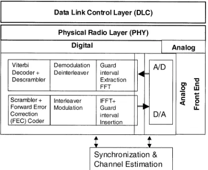
The complete structure of a modem specified by the IEEE 802.11a standard is shown in Fig. 1. It consists of a data
Fig. 1. Block diagram of the physical layer of an IEEE 802.11a compatible modem.
bler, modulator, convolutional encoder, interleaver, 64-point IFFT/FFT, demodulator, deinterleaver, Viterbi decoder, and descrambler. The standard specifies a data rate ranging from 6 to 54 Mb/s. Depending on the desired data rate, the modulation scheme adopted can be binary phase shift keying (BPSK), quaternary phase shift keying (QPSK), or quadrature amplitude modulation (QAM) with 1–6 bit/subcarrier. The encoding rates supported in the standard are 1/2, 2/3, and 3/4. The bandwidth of the transmitted signal is 20 MHz and the OFDM symbol duration is 4 s including 0.8 s for a guard interval [1]. Thus, in effect, FFT/IFFT has to be computed within 4 s.
In general, the FFT implementations typically fall into one of the two categories: 1) methods based on direct Fourier transform [5]–[7] and 2) methods based on direct hardware implementa-tions of established FFT signal flow graphs [8]–[14]. A problem with these solutions is that the approach adopted on the algo-rithmic level typically takes little account of its implications at the architecture, data flow, or chip design levels. Thus, many of these designs [8]–[10] may be irregular, dominated by wiring, and may have heavy overheads in terms of data storage [15]. In a complex system, deployment of such strategies may result in severe disadvantages, because of the tight timing constraints and implicit requirement of low power consumption.
The conventional Cooley–Tukey radix-2 FFT algorithm requires 192 complex butterfly operations for a 64-point FFT computation. Considering that one FFT has to be computed within 4 s, one butterfly operation has to be completed within 20.8 ns which results in 48 MHz clock frequency for a single butterfly architecture. The synthesis result for a radix-2 butterfly unit (one complex multiplication and two complex additions) in IHP 0.25- m technology shows that it occupies 0.18-mm area and dissipates 17 mW power at that frequency. On top of this butterfly unit, one needs memory to store the complex twiddle factors and complex intermediate data, serial-to-parallel and parallel-to-serial converters at the inputs and outputs, respectively, complicated addressing logic and control circuitry. Combining all these circuit modules it is expected that the power dissipation of the entire processor will be quite high. Moreover, the input data arrives at 20 MHz clock frequency, and thus, it is more appropriate to operate the FFT
module at that frequency. In order to satisfy the time constraint at this frequency, one has to employ multiple butterfly units in parallel, which in turn increases the area and power dissipation. Alternatively, since most of the implementations of the IEEE 802.11a standard oversample the incoming data at 40 or 80 MHz, a single radix-2 butterfly based FFT module should be operated at 80 MHz clock frequency (the next available frequency to the actually required frequency). This approach satisfies the timing constraint, but at the cost of high power consumption.
In order to speed up the FFT computation, more advanced so-lutions have been proposed using an increase of the radix [15], [16]. These approaches result in increase of arithmetic com-plexity within the butterfly itself. The radix-4 FFT algorithm is most popular and has the potential to satisfy the current need. However, a single radix-4 butterfly requires three complex mul-tiplications and eight complex additions. Thus, in order to carry out one radix-4 butterfly operation per clock cycle, one needs to complete 12 real multiplications and 16 real additions at each cycle. Since multipliers are typically very power-hungry ele-ments in a VLSI design, this type of arrangement results in sig-nificant power consumption.
More stringent speed limitations are due to the memory access time. For an in-place -point radix- FFT using a single memory bank, read or write RAM accesses are re-quired. In the present case, for a radix-2 conventional FFT this results in a memory access time of approximately 5 ns, which is quite difficult to achieve. As an example, the memory access time for IHP technology is 5.5 ns, which is certainly not suffi-cient for the present purpose. Alternatively, a partitioning of the memory [17] in banks accessed simultaneously, at the price of a complex addressing scheme and higher silicon area can be done.
The main motivation of this work is to derive and investigate an alternative architecture for FFT/IFFT computation that satis-fies the timing constraints stated in the standard IEEE 802.11a with moderate silicon area and low power consumption. Though most of the implementations of the standard oversample the in-coming data at 40 or 80 MHz, we keep our target frequency at 20 MHz, which is the lowest frequency in the baseband data-path. The main reason is that, if an FFT algorithm can satisfy the timing constraint specified in the standard even at this lower frequency, it is expected to be more power efficient compared to the implementations that operate at two or four times higher fre-quency (since power consumption is linearly dependent on the frequency). However, this essentially leads to a reformulation of the FFT algorithm in such a way that the algorithm-to-archi-tecture mapping results in an efficient silicon solution. In Sec-tions III–V, we describe such an approach step-by-step.
III. ALGORITHMICFORMULATION
The discrete Fourier transform (DFT) of a complex data
sequence of length where , can
be described as
where . Let us consider that ,
and , where , and
, . Applying these values in (1) and
simplifying, one gets [18]
(2)
Equation (2) means that it is possible to realize the FFT of length by first decomposing it into one and one -point FFT where , and then combining them. This essentially results in a two dimensional structure instead of a one-dimen-sional structure of FFT. Now considering , one may formulate the 64-point FFT as
(3)
Equation (3) suggests that it is possible to express the 64-point FFT in terms of a two-dimensional structure of 8-point FFTs plus 64 complex interdimensional constant multiplications.
However, since , , the number of required
nontrivial complex multiplications is 49. At first, appropriate data samples (every eighth data of the incoming data se-quence) undergo an 8-point FFT computation followed by eight multiplications with the interdimensional constants or twiddle factors . However, the number of nontrivial multiplications required for each set of 8-point FFT results is actually seven since the zeroth term of the first 8-point FFT gets multiplied with 1. Eight such computations are needed to generate a full set of 64 intermediate data, which once again undergo a second 8-point FFT operation with the appropriate data ordering (every eighth data forms an input data set for the second 8-point FFT). As in the case of the first 8-point FFT, again eight such computations are required. Proper reshuffling of the data coming out from the second 8-point FFT generates the final output of the 64-point FFT.
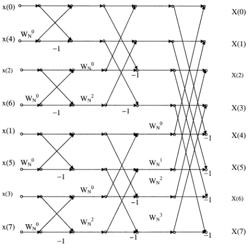
[image:3.612.306.552.60.308.2]The important point to be noted here is that for realization of an 8-point FFT using the conventional decimation in time (DIT) butterfly algorithm, one does not need to use any explicit multiplication operation. This can be shown using the 8-point FFT signal flow graph in Fig. 2. The constants to be multiplied for the first two columns of the 8-point FFT structure are either 1 or and thus, they are mere addition/subtraction operations with the proper data ordering. In the third column, the multiplications of the constants are actually addition/subtraction operation followed by a multiplication of which can be easily realized by using only a hardwired shift-and-add operation. Thus, in principle, an 8-point FFT can be carried out withoutusing anytrue digital multiplier(array multiplier or any type of nonfixed-input multiplier) and thus, provides a way to realize a low-power 64-point FFT at a reduced hardware cost. Since the basic 8-point FFT does not need a true digital multiplier, from (3) one can infer that a complete 64-point FFT computation can be carried out using 49 nontrivial complex multiplications with the interdimensional constants. On the other hand, the number of nontrivial complex multiplications for the conventional 64-point radix-2 DIT FFT is 66. Thus, the present approach results in a reduction of about 26% for complex
Fig. 2. Signal flow graph of an 8-point DIT FFT.
multiplication compared to that required in the conventional radix-2 64-point FFT. This reduction of arithmetic complexity further enhances the scope for realizing a low-power 64-point FFT processor. However, the arithmetic complexity of the proposed scheme is almost the same to that of the radix-4 FFT algorithm since the radix-4 64-point FFT algorithm needs 52 nontrivial complex multiplications.
The IFFT can be performed by first swapping the real and imaginary parts of the incoming data at the primary input, then performing the forward FFT on them and once again swap-ping the real and imaginary parts of the data at the output. This method allows to perform the FFT and IFFT without changing any of the internal coefficients, and thus, results in a more effi-cient hardware implementation.
IV. ARCHITECTURE OF64-POINTFFT/IFFT
The block diagram of the 64-point FFT/IFFT processor de-rived from (3) is depicted in Fig. 3. It consists of an input unit (I/P unit), two 8-point FFT units, a multiplier unit, an internal storage register bank (CBunit), an output unit (O/P unit), and a 5-bit binary counter that acts as the master controller for the entire architecture. However, there are two main performance bottlenecks in such a scheme. First, there is a large number of global wires resulting from multiplexing of the complex data to the 8-point FFTs. Second, the construction of the multiplier unit to attain the required speed with minimal silicon area is not trivial. To eliminate these two bottlenecks and to make ef-ficient algorithm-to-architecture mapping several special strate-gies have been adopted in the current architecture. In the next few subsections, these are explained in detail.
Fig. 3. Block diagram of the proposed 64-point FFT/IFFT processor.
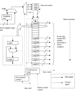
registersreg1,reg2, andreg3 are also provided for temporary storage of data as shown in Fig. 4. The reason for keeping these three temporary storage registers will become clear during our discussion on the multiplier unit. The input unit is equipped with two single-bit signals,modeanddata_start. The assertion of thedata_startsignal indicates the presence of a serial valid data stream at the input of the register bank and subsequently, the input unit starts its operation. Thedata_startsignal remains at logic 1 for the next 64 cycles after its assertion. The logic 1 state of themodesignal indicates the IFFT mode of operation, whereas its logic 0 state indicates the FFT mode. When the modesignal is asserted to the logic 1 state, the real and imagi-nary parts of the input data stream are swapped before the data are serially inputted to the register bank. On the other hand, if themodesignal is at a logic 0 state, the real and imaginary parts of the incoming serial data stream are inputted to the register bank without swapping.
After assertion of thedata_startsignal, at every clock cycle, the input data (16-bit real and 16-bit imaginary) are serially inputted only at the 56th position of the input register bank (reg(56)) and in the successive clock cycles the complex data inside the register bank having index is shifted to the th position where . The input register bank has eight complex 16-bit fixed hard-wired outputs corresponding to the register position index , where . When the input register bank is completely full, the appropriate data (a data octet consisting of every eighth data starting withindex position0), is treated as the input to the 8-point FFT as stated in (3). This data octet in the input buffer automatically gets self-aligned with the hard-wired outputs and is delivered to the first 8-point FFT unit. In the next cycle the same procedure is ex-ecuted once again because of the shifting of the th data sample to the th sample position (this time a data octet consisting of every eighth data starting withoriginal index position1), is treated as the input to the 8-point FFT and so on as described by (3). If this data shifting scheme were not deployed, a par-allel multiplexing scheme for all the 64 complex input data to the 8-point FFT input would be needed. This would result in massive multiplexing and a large number of global connections. With the present scheme the data multiplexing and the number of global connections are substantially reduced. However, this
Fig. 4. Block diagram of the input unit.
downward shifting of data cannot be continued at every clock cycle since the first 8-point FFT does not operate at every clock cycle. This is because; the multiplier unit used here may take more than one clock cycle to process the complete set of data coming from the first 8-point FFT unit. To maintain the correct timing behavior and the pipelined nature of the whole architec-ture, the data are inputted temporarily to one of the three tem-porary registersreg1,reg2, orreg3 when downward shifting of the data is suspended temporarily.
[image:4.612.304.556.262.565.2]control counter by asserting an enable signalStart_count. Once enabled, the master control counter synchronizes the rest of the operations as well as the downward shifting of the data in the input register bankreg(0 to 56).
Eight-Point FFT Units: To construct the 8-point FFT units, we have chosen the radix-2 DIT 8-point FFT algorithm. As was pointed out in Section IV-A1 and shown in Fig. 2, in this case, the butterfly computations are predominantly addition and subtraction operations. We exploited this fact and implemented a fully parallel 8-point FFT architecture by exactly following the flow graph (Fig. 2) using only addition/subtraction and shift-and-add operations. The internal wordlength of these units is 16-bit. The computation of an 8-point FFT is carried out in a single clock cycle.
Multiplier Unit: As stated in Section IV-A2, 49 nontrivial
interdimensional constants are
to be multiplied to the intermediate results coming out from the first 8-point FFT unit. However, a close observation of these constants reveals that only nine sets of them are unique. They are (1,0), (0.995178, 0.097961), (0.980773, 0.195068), (0.956909, 0.290283), (0.923828, 0.382629), (0.881896, 0.471374), (0.831420, 0.555541), (0.773010, 0.634338), (0.707092, 0.707092), where, in each set, the first entry cor-responds to the cosine function (the real part) and the second one corresponds to the sine function (the imaginary part) in the expansion of . The entire interdimensional constant multiplication operation can be carried out using only these nine sets of constants by appropriate swapping of their real and imaginary parts and choosing the appropriate sign. However, the first set of these constants is trivial (1, 0). Thus, in practice, there are eight sets of nontrivial constants required for carrying out the interdimensional constant multiplication operation. The implication is that one requires a storage space for only these eight sets of constants instead of 49. Thus, compared to the conventional DIT FFT algorithm, significantly less storage spacein this scheme is needed.
On the other hand, because of the full parallel implementation of the first 8-point FFT unit the respective computation can be carried out in a single clock cycle, which provides a significant leverage in the overall computation time. However, use of one complex multiplier, operating once in a clock cycle, needs seven clock cycles to complete the interdimensional constant multipli-cation to a full set of data coming out from the first 8-point FFT unit. Thus, the use of a single complex multiplier effectively re-sults in a degradation of the speed advantage provided by the first 8-point FFT unit. To achieve the full speed advantage it is necessary to use seven complex multipliers operating in par-allel. This approach would result in an increased silicon area and high power consumption, and thus, is not a good choice for the present purpose.
A simplified design of the multiplier unit can be done by ex-ploiting the fact that the complex constants to be multiplied are knowna priori. Each of these constants can be realized by de-composing them as a summation/subtraction based on powers of 2. This in essence, results in a shift-and-add architecture for these multiplicative constants. The procedure of multiplication can be explained as follows. If an input data is to be multiplied with a constant 0.995178 (real part of the first set of the
[image:5.612.307.555.59.412.2] [image:5.612.305.552.62.198.2]con-Fig. 5. Circuit diagram of the proposed multiplier.
Fig. 6. Block diagram of the complete multiplier unit.
stant). The constant 0.995178 can be decomposed in terms of
power of 2 as with an accuracy of 26-bit.
Thus, with this representation, the multiplication of with this constant effectively turns into an addition/subtraction of a series of right shifted values of . This is shown in Fig. 5 where the adder at the end may be a single multiple input adder or may be a binary-tree structure of a number of adders. Since the amount of shifts to be introduced to the input are fixed, the shifters shown in Fig. 5 gets reduced to a simple hard-wired connection. The circuitry shown inside the dotted rectangle which consists of the hard-wired shifters and an adder can thus be considered as ahard-wired representation of the constantto be multiplied. This approach can be adopted to carry out the entire multipli-cation operation with limited silicon area and power. For con-venience, from now on, we will refer to this type of circuitry as hard-wired constant.
[image:5.612.306.547.230.411.2]TABLE I
REALIZATION OFDIFFERENTCONSTANTS INTERMS OFPOWER OF2
TABLE II
UTILIZATION OF THEDIFFERENTHARD-WIREDCONSTANTSDURING THE
49 COMPLEXMULTIPLICATIONOPERATION
FFT) one needs to spend only eight clock cycles all together to finish the entire operation. However, in our case, this actually results in a requirement of 12 clock cycles. The four additional clock cycles come from the fact that in the case of some of the multiplication operations, the same hard-wired constant needs to be reused. Table II shows the utilization of these eight hard-wired constants for different sets of data arriving from the first 8-point FFT unit at different time instants. In Table II, for the purpose of simplicity, we assume that the first set of data arrives from the 8-point FFT at zeroth time instant. At different time instants, the hard-wired constants to be used for the multiplication of the incoming data are indicated by 1, whereas 0 indicates the unused hard-wired constants. At the time instant , effectively no multiplication operation is needed as the zeroth block of data (i.e., 8-point FFT output at ) from the 8-point FFT has to be multiplied by (1, 0) and therefore, none of the hard-wired constants are used. The processing of first, third, fifth, and seventh blocks of data (i.e., 8-point FFT output at and ) requires one clock cycle each where all hard-wired constants exceptConst8 are involved in the multiplication process. On the other hand, the processing of second and sixth block of data (i.e., 8-point FFT output at and ) requires two cycles each. This is due to the fact that Const2, Const4 and Const6 are reused two times in successive clock cycles for the complex multiplication operation. For processing the fourth block of data, one needs to spend four clock cycles asConst4 is reused four times, whereas Const8 is reused two times. Thus, the data coming out of the first 8-point FFT block at even time instants has to be kept for more than one clock cycle until the multiplication of the full set is completed. A straightforward strategy to do this is to suspend
the operation of the 8-point FFT unit during those clock cycles. This also implies a suspension of downward shifting of the data in the input unit for those clock cycles. However, upon completion of the complex multiplication for the respective set of 8-point FFT data; the downward shifting of the data in the input register bank and the 8-point FFT operation resumes once again. To keep the data flow intact, we have introduced the three temporary registers (as mentioned earlier) at the input that hold the incoming data like a FIFO when the downward shifting of data in the input register bank is temporarily suspended.
To give an impression about the area and power saving, this hard-wired-constant-based multiplier unit is compared to a mul-tiplier unit that consists of eight complex mulmul-tipliers in par-allel. To perform this comparison, we synthesize the multiplier unit described above and a multiplier unit consisting of eight complex multipliers in IHP 0.25- m BiCMOS technology at 20 MHz operating frequency and 2.5 V supply voltage. The cell area and the average power consumption of the hard-wired-con-stant-based multiplier described here are 0.6 mm and 19 mW, respectively. The same parameters for the multiplier unit having eight parallel complex multipliers are 1.1 mm and 33 mW, respectively. Thus, the adopted approach needs approximately 45% less cell area and 42% less power compared to the later one.
Apart from these eight sets of hard-wired constants, the mul-tiplier unit also has two 8-to-8 16-bit complex shuffle networks at its input and output, respectively, as shown in Fig. 6. The input shuffle network routes the data from the first 8-point FFT unit to the appropriate hard-wired constants (Const1,…,Const8) and the output shuffle network maps the multiplied data to the ap-propriate index position of the internal storage register bankCB. Internal Register Bank (CB): The internal register bank (CB) is of 16-bit wordlength and is used for temporary storage of the 64 complex data coming from the multiplier unit. Similar to the input register bank, it has eight hard-wired outputs corre-sponding to the registers having the positional indices where . These outputs are directly connected to the input of the second 8-point FFT unit. Once the register bank of theCBunit is filled, the data at the th position is shifted to the th position at every clock cycle, where . This downward shift essentially means that at every clock cycle the appropriate data [according to (3)] at the output of theCB unit gets self-aligned with the input of the second 8-point FFT unit. Since the second 8-point FFT unit computes a full set of re-sults in one clock cycle, this downward shifting of data occurs at every clock cycle and takes place for the next eight cycles after theCBregister bank is full. Construction-wise, theCBunit is similar to the input unit except no extra registers and swapping unit are needed.
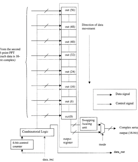
Fig. 7. Block diagram of the output unit.
the new data arrives from the second 8-point FFT unit at the th positions of the output register bank, the old data corresponding to those positions are shifted downwards by one position and the data output mechanism proceeds in the same way.
To control the data output from the output unit, a 6-bit internal counter is used. This counter is enabled with the assertion of the signaldata_indgenerated by the master control counter and counts up to 63 until the last output data is available at the serial output. Additionally, adata_outsignal is also generated when the data_ind signal is asserted. This signal essentially means that the zeroth position of the output register bank is filled and valid output data will be available from the next clock cycle. After assertion, this signal remains in the logic 1 state for the next 64 cycles.
The output unit shares themodesignal with the input unit. When themodesignal is in the logic 1 state, the real and imag-inary parts of the output data are first swapped and then scaled down by 64 using a 6-bit right shift. The resulting data gives the result of an IFFT. When the modesignal is 0, the output unit outputs the data in the FFT mode by keeping the real and imag-inary parts of the output as they are.
The Control Mechanism: The controller for the overall architecture is a simple 5-bit binary counter. The counter starts counting from 0 with the assertion of the signal Start_count from the input unit, when the 56th position of the input register bank is filled. At count number 16, the first output data is available at the zeroth position of the output register bank. At this point, thedata_indsignal is asserted by the control counter that enables the serial data output mechanism by activating the output control counter. All required internal computation is completed and the complete set of output data is stored in
Fig. 8. Synthesized cell area of different constituent blocks of the 64-point FFT/IFFT processor.
the output register bank when the count of the master control counter reaches 23. At this point the master control counter is reset to zero and can be reactivated when the next set of input data fills the 56th position of the input register bank. However, in the mean time, the output control counter of the output unit controls the serial data output mechanism.
V. CHIPDESIGN
A. Design Flow
The architecture was first modeled in VHDL and functionally verified using Mentor Graphics’ Modelsim simulator. The out-puts from the VHDL coded architecture are validated against a standard C-coded FFT routine. According to the specifica-tion stated in Secspecifica-tion I, a clock frequency of 20 MHz is used. The input data are delivered to the processor in a serial manner. The latency of the processor is 3.85 s, i.e., 77 clock cycles. The parallel to parallel (i.e., the basic 64-point FFT compu-tation, assuming parallel input data and parallel output data) FFT/IFFT computation requires 1.15 s, i.e., 23 clock cycles. The throughput rate of the architecture is one complete set of 64-point FFT/IFFT (provided as serial output) in 3.2 s, i.e., 64 cycles. The minimum time interval between two successive sets of input data (i.e., last data of the previous set and the first data of a new set) for which the architecture shows correct functional behavior is equal to three clock cycles.
After functional validation, the architecture was synthesized for IHP 0.25- m three-metal layer BiCMOS technology using the Synopsys Design Analyzer. The synthesized circuit was then back-annotated using the Modelsim simulator, showing the correct functional behavior. The synthesized cell area of the complete processor is 3.6 mm . The cell area requirement for the different blocks of the design is shown in Fig. 8 where the combined area of the hard-wired multiplier unit, its input/output shuffle network and the internal storage register bank CB is represented in one block termed as complex_mult unit. The combined cell area of all the other data shuffling networks are denoted asshuffleand the area requirement for the master control counter is denoted ascounterin Fig. 8. As expected, the complex_mult unit consumes the largest cell area.
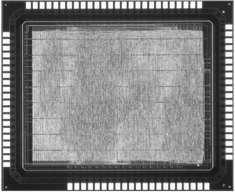
[image:7.612.306.553.62.214.2]Fig. 9. Die photograph of the fabricated 64-point FFT/IFFT processor.
6.8 mm and the complete area including power rings and I/O pads is 13.5 mm . The processor has 85 I/O pins of which 36 are input pins and 33 are outputs. The rest of the pins are used for power supply. The die photograph of the fabricated chip is shown in Fig. 9.
B. Test Strategy
The inherent linear structure of the architecture greatly sim-plifies the testing of the chip. We adopted the conventional full scan test for the chip. Existing flip-flops were replaced byscan flip-flopsduring the synthesis phase. The complete design con-tains 7134 scan flip-flops. Test vectors were generated using the Synopsys test manager. As reported by the Synopsys test manager, 99% fault coverage has been achieved. To enable the scan test, two external input pins termed as scan_enableand scan_inare provided. The outputscan_outpin is merged with the most significant bit of the real component of the output reg-isterout(56).
C. Measurement Results
The designed FFT/IFFT processor was fabricated in-house using the IHP 0.25- m BiCMOS process. The chips were pack-aged in a QFP100 package. Testing was carried out using the IHP chip tester (HP93000 SoC). For functional tests, precalcu-lated data vectors were fed to the chip in a continuous manner and the output was checked while operating the chip at 20 MHz frequency. This test validates the functional behavior of the chip. After the functional test, a test for maximum allowable fre-quency of operation was carried out. The measurement result shows that at 2.5 V supply voltage the chip exhibits correct func-tional behavior up to 38 MHz. The average power dissipation of the processor measured over 55 fabricated chips is 84 mW at 2.5 V and 20 MHz clock frequency.
In the second phase, the function of the chip was tested at lower supply voltage. It was found that the chips operate cor-rectly down to 1.8 V supply voltage. However, the maximum allowable frequency in this case is 26 MHz, which still satis-fies our target frequency. The average power consumption of the processor at 1.8 V supply voltage at 20 MHz frequency is
41 mW. These figures suggest that the designed processor is a good candidate for low-power high-speed applications.
In the third phase, the scan test was carried out using the vector set generated by the Synopsys test manager. This is done by operating the processor in thescan mode. Vector data generated by Synopsys test manager are directly translated to the tester format. In this mode of operation, parallel vectors are inputted to the processor for three successive cycles (capture cycles) and in the next cycle, a scan operation is carried out (scan instance). Each of the scan instances needs 7134 cycles (the number of flip-flops in the design). During scan operation, the scan_out pin is compared with the expected value. 416 scan instances are performed with 1657 parallel vectors which gave a correct result.
D. Main Features and Comparison
The algorithm-to-architecture mapping in the present design was done with the aim to reduce multiplexing and attendant global wirings. The strategy of downward shifting of the data in conjunction with the self-alignment of it to the fixed hard-wired connections at the input and output register bank effectively re-duces the multiplexing and global wiring compared to the con-ventional implementation by a factor of 64 and 8 at the input and output of the input unit, a factor of 8 at the input and output of theCBunit and a factor of 8 and 64 at the input and output of the output unit. This massive reduction of signal multiplexing and global wiring implies a better utilization of silicon area, re-duction of routing overhead, and lower power consumption. The effectiveness of the algorithm-to-architecture mapping method-ology adopted here can be better appreciated considering the following comparison.
In [3] and [19], we proposed a different design of the 64-point FFT processor using the same principal algorithm presented here. In both cases, the design utilizes only one 8-point FFT processor. The input data to the 8-point FFT processor and the intermediate results after multiplication with the interdimensional constants are stored in a single bank of registers. Binary multipliers were used to carry out the complex multiplication operations. The synthesized cell areas of both earlier reported architectures are approximately equivalent to 81 k inverter gates in our in-house technology. Compared to those designs, the synthesized cell area of the present design is equivalent to 123 k inverter gates. However, though the cell area of the present design is about 34% higher than the previous ones, the real advantage of the present one is visible on the layout level. The core area of the present implementation after layout is 6.8 mm , whereas the same parameter for the referenced designs is approximately 18 mm for the same technology. Thus, the present architecture exhibits superior quality of silicon area utilization compared to the referenced designs even though its cell area is higher.
TABLE III
THEPERFORMANCECOMPARISON OF THEPROPOSEDFFT/IFFT PROCESSOR
WITH THECOMMERCIALLYAVAILABLE64-POINTFFT/IFFT IP CORES
TABLE IV
THEPERFORMANCECOMPARISON OF THEPROPOSEDDESIGNWITH
AVAILABLECHIPSETS FORCOMPUTING64-POINTFFT/IFFT
is expected to be less power hungry than the others. However, at present, the proposed architecture is not configurable as are some of the available IP cores since it is designed for a specific application.
The superiority of the proposed processor is also evident from Table IV where the comparison with several other commercially available and reported ASIC chips is done. This comparison shows that the proposed processor needs the smallest number of processing cycles and silicon area and consumes the least power compared with the others.
VI. CONCLUSION
A novel 64-point FFT/IFFT architecture for high-speed WLAN systems based on OFDM transmission has been presented. This architecture is based on a decomposition of the 64-point FFT into two 8-point FFTs so that the resulting algorithm-to-architecture mapping is well suited for silicon implementation. It exhibits numerous attractive features from a VLSI point of view, which include regularity, modularity, simple wiring, and high throughput.
A new low-power high-performance 64-point FFT/IFFT chip for WLAN applications has been successfully designed and fab-ricated based on the architecture described. The chip includes all necessary interfaces to directly integrate it with the other datapath elements for an IEEE 802.11a modem or similar ap-plications. The chip computes a 64-point parallel to parallel FFT/IFFT in 23 clock cycles, yet only dissipates 41 mW power at 20 MHz clock frequency and at 1.8 V supply voltage. The new chip is deemed to result in a considerable reduction in cost, size, and power dissipation for the existing WLAN sys-tems. The work undertaken demonstrates how combining higher
level system requirements with efficient algorithm-to-architec-ture mapping strategies can produce efficient silicon solutions for high-performance WLAN systems.
REFERENCES
[1] Draft Supplement to Standard [for] Information Technology-Telecom-munications and Information Exchange Between Systems—Local and Metropolitan Area Networks-Specific Requirements—Part 11: Wireless LAN Medium Access Control (MAC) and Physical Layer (PHY) Specifications: High Speed Physical Layer in the 5 GHz Band, IEEE P802.11a/D7.0.
[2] T. Xanthopoulos and A. P. Chandrakasan, “A low-power IDCT macro-cell for MPEG-2 MP@ML exploiting data distribution properties for minimal activity,”IEEE J. Solid-State Circuits, vol. 34, pp. 693–703, May 1999.
[3] E. Grass, K. Tittelbach, U. Jagdhold, A. Troya, G. Lippert, O. Krueger, J. Lehmann, K. Maharatna, N. Fiebig, K. Dombrowski, R. Kraemer, and P. Maehoenen, “On the single chip implementation of a hiperlan/2 and IEEE802.11a capable modem,”IEEE Pers. Commun., vol. 8, pp. 48–57, Dec. 2001.
[4] K. Maharatna, E. Grass, and U. Jagdhold, “A novel 64-point FFT/IFFT processor for IEEE 802.11a standard,” inProc. ICASSP’03, vol. II, pp. II-321–II-324.
[5] C. Chen and L. Wang, “A new efficient systolic architecture for the 2-D discrete Fourier transform,” inProc. IEEE Int. Symp. Circuits and Sys-tems, vol. 6, ch. 732, 1992, pp. 689–692.
[6] M. Ghouse, “2D grid architectures for the DFT and the 2D DFT,”J. VLSI Signal Process., vol. 5, pp. 57–74, 1993.
[7] H. Lim and E. Swartzlander, “A systolic array for 2-D DFT and 2-D DCT,” inProc. Int. Conf. Application Specific Array Processors, 1994, pp. 123–131.
[8] N. Zhang, X. Zhang, and C. Zhang, “Two kinds of array architecture for FFT processor,” inProc. Int. Conf. Signal Processing, vol. 2, ch. 355, 1990, pp. 1161–1162.
[9] J. Muller and D. Trystram, “Perfect shuffle VLSI implementation: Ap-plications to sorting and FFT computation,” inProc. CONPAR ’88, pp. 197–204.
[10] B. Gold and T. Bially, “Parallelism in fast Fourier transform hardware,”
IEEE Trans. Audio Electroacous., vol. 21, pp. 5–16, Feb. 1973. [11] E. Bidet, D. Castelain, and P. Senn, “A fast single-chip implementation
of 8192 complex point FFT,”IEEE J. Solid-State Circuits, vol. 30, pp. 300–305, Mar. 1995.
[12] E. Swartzlander, V. Jain, and H. Hikawaka, “A radix-8 wafer scale FFT processor,”J. VLSI Signal Processing, vol. 4, pp. 165–176, 1992. [13] H. Yeh, “Highly pipelined VLSI architecture for computation of fast
fourier transforms,”Proc. SPIE, vol. 2027, pp. 112–121, 1993. [14] V. Szwarc and L. Desormeaux, “A chip set for pipeline and parallel
pipeline FFT architectures,” J. VLSI Signal Processing, vol. 8, pp. 253–265, 1994.
[15] C. W. Hui, T. J. Ding, and J. V. McCanny, “A 64-point Fourier transform chip for video motion compensation using phase correlation,”IEEE J. Solid-State Circuits, vol. 31, pp. 1751–1761, Nov. 1996.
[16] R. Bhatia, M. Furuta, and J. Ponce, “A quasi radix-16 FFT VLSI processor,” inProc. IEEE Acoustics, Speech, and Signal Processing (ICASSP), Apr. 1991, p. .
[17] J. O’Brien, J. Mather, and B. Holland, “A 200 MIPS single-chip 1K FFT processor,” inIEEE Solid-State Circuits Conf. (ISCCC) Dig. Tech. Papers, Feb. 1989, pp. 166–167, 327.
[18] A. M. Despain, “Very fast Fourier transform algorithms hardware for implementation,”IEEE Trans. Comput., vol. C-28, no. 5, pp. 333–341, 1979.
[19] K. Maharatna, E. Grass, and U. Jagdhold, “A low-power 64-point FFT/IFFT architecture for wireless broadband communication,” in
Proc. 5th Int. OFDM Workshop, Hamburg, Germany, Sept. 2000, p. 36. [20] Xilinx Product Specification, High-Performance 64-Point Complex FFT/IFFT V1.0.5 [Online]. Available: http://www.xilinx.com/ipcenter [21] Altera Megafunction Technical Brief ISS High-Performance 64-Point
FFT/IFFT [Online]. Available: http://www.spinnaker.co.jp/jp/datasheet/ tb_fft_1_V002.pdf
[22] Product Design Data Sheet, FFT-1024 Complex 1024-Points FFT/ IFFT Processor. Icomm Technologies Inc. [Online]. Available: www. icommtech.com/Products/FFT-64.PDF
[24] J. V. McCanny, D. Trainor, Y. Hu, and T. J. Ding. Rapid design of com-plex DSP cores. [Online]. Available: http://www.esscirc.org/papers-97/ 102.pdf
[25] T. Chen and L. Zhu, “An expandable column FFT architecture using circuit switching network,”J. VLSI Signal Process., vol. 6, no. 3, pp. 243–257, Dec. 1993.
[26] T. Chen, G. Sunanda, and J. Jin, “COBRA: A 100-MOPS single-chip programmable and expandable FFT,”IEEE Trans. VLSI, vol. 7, pp. 174–182, June 1999.
Koushik Maharatna received the M.Sc. degree from Calcutta University, India, and the Ph.D. degree from Jadavpur University, India, in 1995 and 2002, respectively.
From 1996 to 2000, he was involved in projects sponsored by the Government of India undertaken at the Indian Institute of Technology (IIT), Kharagpur. From 2000 to 2003, he was working as a Scientist at IHP GmbH. His main involvement in IHP was related to the single-chip implementation of the IEEE 802.11a standard. In August 2003, he joined the Department of Electrical and Electronic Engineering, University of Bristol, Bristol, U.K., where he is currently a Lecturer. His research interests include computer arithmetic, architectural design for DSP and communication processes, and ASIC design.
Eckhard Grassreceived the Dr.-Ing. degree in elec-tronics from the Humboldt University Berlin, Ger-many, in 1992.
He was a Visiting Research Fellow at Lough-borough University, U.K., from 1993 to 1995, and a Senior Lecturer in microelectronics at the University of Westminster, London, U.K., from 1995 to 1999. Since 1999, he has been with IHP GmbH, Frankfurt (Oder), Germany, leading a project on the implementation of a wireless broadband communication system. One major aim of this project is to implement a complete 5-GHz WLAN modem on a single chip. His research interests include data-driven (asynchronous) signal processing structures and low-power VLSI implementation of communication systems.
Ulrich Jagdholdreceived the Diploma in physics (M.Sc. degree) from Dresden Technical University, Germany, in 1987.