FIELD INDUCED EVOLUTION OF REGULAR AND RANDOM 2D DOMAIN STRUCTURES AND SHAPE OF ISOLATED DOMAINS IN LiNbO3 AND LiTaO3
A.I. Lobov1, V.Ya. Shur1, I.S. Baturin1, E.I. Shishkin1, D.K. Kuznetsov1, A.G. Shur1,
M.A. Dolbilov1, and K. Gallo2
1 Ferroelectric Laboratory, Ural State University, 620083 Ekaterinburg, Russia
2 Optoelectronics Research Centre, University of Southampton, SO17 1BJ, UK
Abstract
The shapes of isolated domains produced by application of the uniform external electric field
in different experimental conditions were investigated experimentally in single crystalline lithium niobate LiNbO3 and lithium tantalate LiTaO3. The study of the domain kinetics by
computer simulation and experimentally by polarization reversal of the model structure using two-dimensional regular electrode pattern confirms applicability of the kinetic approach to explanation of the experimentally observed evolution of the domain shape and geometry of
the domain structure. It has been shown that the fast domain walls strictly oriented along X directions appear after domain merging.
Keywords: domain structure, polarization reversal, lithium niobate, lithium tantalate, domain kinetics
INTRODUCTION
Recently the periodically poled (PP) nonlinear optical ferroelectric crystals are developed for usage in coherent light sources based on quasi-phase matching [1-3].Lithium niobate LiNbO3 (LN) and lithium tantalate LiTaO3 (LT) are the most popular materials due to
their record electro-optical and nonlinear optical coefficients. The tailored domain structures are produced by application of electric field to lithographically defined electrode patterns
[4,5]. Therefore the kinetic of the domain structure during poling including the evolution of the isolated domain shape has to be controlled precisely. The knowledge of the domain shape evolution in adjusted switching conditions will allow to specify the shape of individual
domains in two-dimensional (2D) periodically poled domain structures in LN and LT thus opening the new stage in micro-scale domain engineering important for manufacturing of the
photonic crystals. Moreover the study of the domain shape dependence on experimental conditions for switching in uniform electric field is very important for revealing the main laws of the phase growth during any first order phase transition. In this case the domain
structure presents the useful model system and its evolution in electric field can be used for direct study of the phase transformation kinetics.
In this paper the detailed experimental study of the domain shape in LN and LT during
polarization reversal observed in various experimental conditions is presented. Computer simulation of isolated domain enlarging based on generation and subsequent growth of
elementary steps at the domain walls allows us to explain the origin of various unusual experimentally observed shapes. Evolution of the domain shape after merging of neighboring domains was investigated in periodical two-dimensional model structure both experimentally
Shapes of isolated domains
All crystals of LN/LT family are uniaxial ferroelectrics representing C3V symmetry in
polar phase thus possessing the simplest domain structure with 180O domain walls only. It was stated that the shapes of isolated domains, formed under application of electric field in
these crystals, are regular hexagonal and triangular prisms or truncated pyramids [6,7]. Usually, the investigation is carried out by observation of the domains revealed by etching at the polar surfaces. Thus the usually discussed regular polygonal shapes of isolated domains in
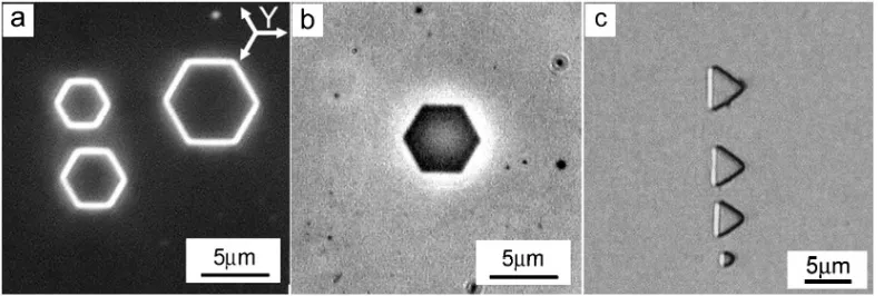
LN and LT correspond to the shape of cross-sections of the domain by the polar surface. It was stated that in LN only hexagons with orientation of the domain walls along Y
[image:3.595.101.498.408.541.2]crystallographic directions are allowed (Fig. 1a). While in LT, the shape changes drastically from triangular with X oriented walls in congruent (CLT) (Fig. 1b) to hexagonal with Y oriented walls in stoichiometric (SLT) [8] (Fig. 1c).
Figure 1. Classical shapes of individual domains for (a) CLN, (b) SLT,(c) CLT. Visualization by optical microscopy: (a) dark field, (b) phase contrast, (c) bright field. (a), (c) domains
revealed by chemical etching.
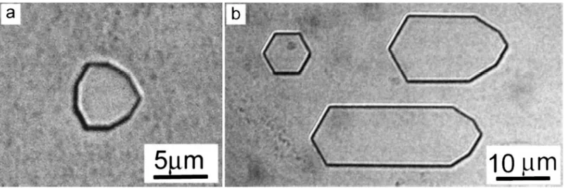
It is known that the shape of individual domain in real experimental situations depends
on the switching conditions and can drastically deviate from the classical one (regular polygons) (Fig. 2). Nevertheless the dependence of the domain shape on the polarization
Figure 2. Variants of real shapes of individual domains in CLN. The domains were revealed by chemical etching and visualized by optical microscopy.
Dependence of isolated domains shapes on switching conditions
The evolution of the domain structure during polarization reversal was in situ recorded using polarized microscopy. The static domains patterns revealed by selective chemical etching were visualized using optical and atomic force microscopy.
It was shown that the classical hexagonal shape domains with walls strictly oriented along crystallographic directions appear only during very slow (“equilibrium”) polarization reversal when the screening of depolarization field (Edep) is almost complete. It was shown by us that a degree of deviation from equilibrium conditions during domain growth can be characterized by the ratio between screening and switching rates [9,10].
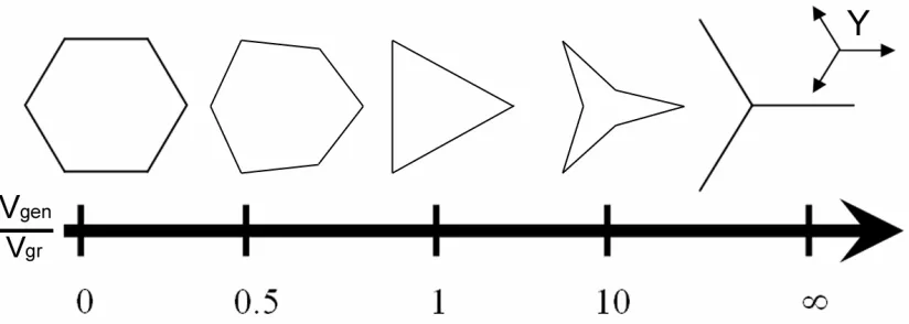
Figure 3. Simulated diagram of the domain shape dependence on the ratio of step generation to step growth rates.
Computer simulation of the isolated domain growth
We have studied the growth of isolated domains in crystals with С3 symmetry by computer simulation using modified cellular automaton. All calculations were made on the basis of the kinetic approach to domain structure evolution proposed by us earlier [11,12]. For explanation of the domain shape we have considered the classical model of sideways domain wall motion by generation of elementary steps (depth about one unit cell) at the domain wall (2D nucleation) and their subsequent growth by 1D nucleation [13-15]. We have discovered experimentally by direct observation of the domain growth that the nucleation process is essentially anisotropic. It was shown that the step generation is observed only on three discontiguous vertexes of the hexagonal domain in Y+ direction [9,10]. It is convenient to characterize the step generation rate by experimentally measured vertex motion velocity Vgen, and the step growth – by motion velocity of the step edge Vgr. Under equilibrium switching conditions Vgen << Vgr and domain shape remains perfectly hexagonal. However, under non-equilibrium conditions Vgen can essentially exceed Vgr thus leading to deviation of the wall orientations from Y directions.
The simulation of the domain growth for wide range of Vgen/Vgr values allows us to obtain the smooth variation of the domain shapes from equilateral hexagon to stars with three domain rays (Fig. 3). It is clear that all discussed domain shapes are in accordance with the crystal symmetry.
Figure 4. Experimentally observed predicted domain shapes in CLN for switching with artificial dielectric layer : (a) irregular convex hexagon, (b) concave hexagon (“Mercedes star”), (c) rays triplet (“claw”). The domains were revealed by chemical etching and visualized by
optical microscopy
Domain shape evolution during merging
We have studied experimentally the domain shape evolution after merging of several hexagonal domains. It was shown that the merging of two Y oriented domain walls leads to formation of the X oriented wall. The essentially higher velocity of X walls as compare with Y walls leads to their limited lifetime. Nevertheless the switch off of the external field allows to fix the unusual domain shapes – polygons with both Y and X walls.
Application of the computer simulations for study of the domain shape evolution after merging allowed us to obtain all experimentally observed “abnormal” shapes and to explain formation of convex polygonal domains with wall number ranged from 6 to 12. The simulation shows that the merging of two Y domain walls leads to formation of strictly oriented X wall.
It is known that the sideways wall motion velocity is determined by generation rate of the elementary steps. Thus the abnormally high velocity of X walls, as compare with Y ones, is caused by the maximum possible density of the elementary steps, which remains during whole lifetime (Fig. 5). Appearance of X walls increases the number of the sides of any polygonal domain.
Figure 5. (a) Scheme of X domain wall with maximum step concentration. (b) Scheme demonstrating subsequent positions of X domain wall after merging.
It is necessary to point out that the concave domain shape appears just after the merging of two convex ones (Fig. 6a). Such unusual temporary shape transforms in short time to the convex one due to fast motion of X wall. Thus X wall length increases after merging (on the stage of concave domain) and decreases to total disappearance after formation of convex domain leading to formation of the single hexagonal domain with Y walls only (Fig. 6b).
[image:7.595.124.486.227.396.2](c)
Figure 6. Evolution of the domain shape after merging from (a) concave to (b) convex stages, and (c) corresponding change of the X domain wall length.
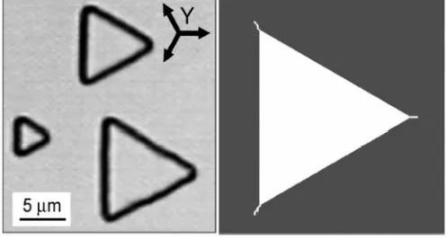
[image:7.595.186.434.608.741.2]Figure 7. Triangular domain shape. (a) domains in CLT revealed by chemical etching and visualized by optical microscopy, (b) simulation results for Vgen/Vgr ≥ 1.
The complete evolution of the domain shapes as a result of merging of two hexagonal domains with Y walls only ((Y)convex) can be presented by the following scheme:
(Y)convex + (Y)convex => (Y + X)concave => (Y + X)convex => (Y)convex
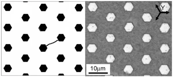
The experimental study of the domain shape evolution during merging has been done for regular 2D domain structure produced by the hexagonal grid electrode pattern. The merging of individual domains has been stimulated by artificial conducting defects between neighboring electrodes (“bridges”). The domain evolution after merging was studied in details both experimentally and by computer simulation (Fig. 8).
Figure 8. (a) Regular 2D electrode structure with conductive bridge used for computer simulation, (b) domain structure produced by 2D electrode pattern in CLN.
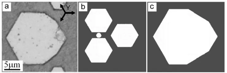
[image:8.595.161.464.310.445.2]In the framework of proposed model we have considered several variants of neighboring domain merging for different number of simultaneously merged domains. It has been shown that after simultaneous merging of three domains the shape of the formed convex domain is the regular nonagon (Fig. 9). Such shape has been found experimentally. It is interesting that the regular nonagon can be produced also using triangular shape electrode.
[image:8.595.115.478.594.715.2]It is seen that the consequent merging leads to decreasing of the side number in convex domain polygon because during non-simultaneous domain merging the X wall which appears first will disappear due to its limited lifetime before formation of the convex polygon (Fig. 10). It is clear that, such situation is much frequently realized experimentally and octagonal domains are easily observed.
[image:9.595.122.492.182.302.2]Figure 10. Formation of octagonal domain after consequent merging of three hexagonal domains:
(a) experiment, (b) and (c) computer simulation.
The maximum predicted number of the sides in domain polygon is 12, but it is difficult to obtain such a shape because it can appear only as a result of simultaneous merging of six domains. Nevertheless all polygon domain shapes with side number ranging from 6 to 12 has been experimentally observed and can be produced artificially with specified electrode structure.
CONCLUSIONS
of these walls is the fastest due to the maximal possible step concentration remaining during the whole lifetime of X wall. It allows to explain experimentally observed domain shapes with mixture of Y and X – walls with right angles, whose existence seems to contradict the crystal symmetry.
It is important that in both cases the model allows to reconstruct the kinetics of domain formation and to choose the switching conditions for formation of proper domain shapes. The last fact allows to use this approach while manufacturing the 2D periodical domain structures with tailored shapes in lithium niobate and lithium tantalate.
The research was made possible in part by Grant 03-51-6562 of INTAS; by Grant 04-02-16770 of RFBR; by Grant 03-02-39004 of NNSF; by Grant 04-02-04007 of RFBR-DFG and by Grants 48859, 49130 and RNP 2.1.1.8272 of Program "Development of the Scientific Potential of High Education”, by Grant MK-2434.2005.2 of President Program of Federal Agency of Education; by PhD Award Y1-P-05-20/4146 of the U.S. CRDF BRHE and Federal Agency of Education, by Grant RUE1-5037-EK-04 of CRDF FSTM
References
[1] J. Chen, Q. Zhou, J. Hong, W. Wang, N. Ming, D. Feng, and C. Fang, J. Appl. Phys. 66, 336 (1989).
[2] R.L. Byer, J. Nonlinear Opt. Phys. & Mater. 6, 549 (1997).
[3] G. Rosenman, A. Skliar, and A. Arie, Ferroelectrics Review 1, 263 (1999).
[4] M. Yamada, N. Nada, M. Saitoh, and K. Watanabe, Appl. Phys. Lett. 62, 435 (1993). [5] R. Batchko, V. Shur, M. Fejer, and R. Byer, Appl. Phys. Lett. 75, 1673 (1999).
[6] N. Ohnishi and T. Izuka, J. Appl. Phys. 46, 1063 (1975). [7] V. Gopalan and M. Gupta, Appl. Phys. Lett. 68, 888 (1996).
[8] K. Kitamura, Y. Furukawa, K. Niwa, V. Gopalan, and T. Mitchell, Appl. Phys. Lett. 73, 3073 (1998).
[9] V.Ya. Shur, in “Nucleation Theory and Applications”, Ed. by J.W.P. Schmelzer, WILEY-VCH, 2005, Ch.6, 178;
[10] V.Ya. Shur, J. Materials Science, 41, 199 (2006).
[11] V.Ya. Shur, E.V. Nikolaeva, E.I. Shishkin, A.P. Chernykh, K. Terabe, K. Kitamura, H. Ito, and K. Nakamura, Ferroelectrics, 269, 195 (2002).
[12] V.Ya. Shur, E.V. Nikolaeva, E.I. Shishkin, V.L. Kozhevnikov, A.P. Chernykh, K. Terabe, and K. Kitamura, Appl. Phys. Lett. 79, 3146 (2001).
[13] R.C. Miller and G. Weinreich, Phys. Rev. 117, 1460 (1960). [14] M. Hayashi, J. Phys. Soc. Jap. 33, 616 (1972)