University of Southern Queensland
Faculty of Health, Engineering and Sciences
Modelling and analysis of multi-junction
photovoltaic cells using MATLAB/Simulink for
the improvement of conversion efficiency.
A dissertation submitted by
Anthony Laurent
in fulfilment of the requirements of
ENG4111 and 4112 Research Project
towards the degree of
Bachelor of Engineering (Honours) (Electrical)
i
Abstract
Multijunction solar cells (MJSCs) are a more efficient photovoltaic solar cell technology than the
conventional single junction alternative. When used in conjunction with concentrator technology
MJSCs can provide conversion efficiencies upwards of 40% - due to a better conversion response
to a broader light spectrum. Iterative design methodology can be applied to derive models of
conversion efficiency in MJSCs by adapting existing single junction solar cell (SJSC) modelling
practices. However this can be a very time consuming process, given the abundance of literature
regarding conversion efficiency in SJSCs
This dissertation provides several criteria to consider when designing MJSC conversion efficiency
models, by addressing two research questions: (1) how is the conversion efficiency of MJSCs
simulated within the Matlab/Simulink environment?, (2) and which of the existing SJSC modelling
practices are more/less adaptable for simulating MJSCs in the Simulink environment.
The first part of the literature review outlines the peer reviewed literature regarding SJSC model
practices and discusses the results of the project simulation tests. The second part of the review (1)
outlines the literature on MJSC architecture related to model design, (2) proposes an iteration of a
SJSC model that simulates the conversion efficiency in MJSCs and (3) discusses the results of the
proposed model tested under Simulink simulation.
The simulation results confirmed that, as expected, the double diode model provides more accurate
results than the single diode model, with respect to changes in temperature and changes in
irradiance. The simulation results confirmed that the proposed model correctly simulated the
conversion efficiency in MJSCs with respect to irradiance, but failed to correctly simulate the
conversion efficiency in MJSCs with respect to temperature.
This paper offers insight into appropriate and inappropriate SJSC modelling techniques to consider
when applying iterative design methodology to design a model that correctly simulates MJSC
ii
University of Southern Queensland
Faculty of Health, Engineering and Sciences
ENG4111 & ENG4112 Research Project
Limitations of Use
The Council of the University of Southern Queensland, its Faculty of Health, Engineering &
Sciences, and the staff of the University of Southern Queensland, do not accept any responsibility
for the truth, accuracy or completeness of material contained within or associated with this
dissertation.
Persons using all or any part of this material do so at their own risk, and not at the risk of the
Council of the University of Southern Queensland, its Faculty of Health, Engineering & Sciences
or the staff of the University of Southern Queensland.
This dissertation reports an educational exercise and has no purpose or validity beyond this
exercise. The sole purpose of the course pair entitled “Research Project” is to contribute to the overall education within the student’s chosen degree program. This document, the associated
hardware, software, drawings, and other material set out in the associated appendices should not be
iii
Certification
I certify that the ideas, designs and experimental work, results, analyses and conclusions set
out in this dissertation are entirely my own effort, except where otherwise indicated and
acknowledged.
I further certify that the work is original and has not been previously submitted for assessment in
any other course or institution, except where specifically stated.
Anthony Laurent
iv
Acknowledgements
It would not have been possible to complete this dissertation, let alone my undergraduate studies, if
my lovely wife Kristen had not been so unflinchingly supportive. My two fantastic kids and loving
parents also deserve a very heart-felt thanks
Many thanks to my Principal Supervisor, Dr Narottam Das, for providing me with this research
opportunity - I have learned a great deal throughout this project. I would like to express my
sincerest gratitude to my project Co-supervisor, Mr Andreas Helwig, whose guidance and support
will not be forgotten by myself or Kristen. I am also grateful to Dr Les Bowtell and Associate
v
Table of Contents
Abstract ... i
Limitations of Use ... ii
Certification ... iii
Acknowledgements ... iv
Table of Figures ... ix
List of Tables ... xi
Nomenclature ... xiii
Chapter 1:
Introduction ... 1
1.1. Context ... 1
1.2. Problem Specification ... 1
1.3. Aim and objectives ... 1
1.4. Dissertation Overview ... 2
Chapter 2:
Literature Review ... 3
2.1. The conventional single junction silicon solar cell ... 3
2.1.1. The P-N junction diode ... 4
2.1.2. Bandgap energy model ... 5
2.2. The photodiode based solar cell model ... 6
2.3. Ideal photodiode and characteristic curves ... 7
2.3.1. Solar cell characteristics ... 9
2.3.1.1 Short circuit current ... 10
2.3.1.2 Open circuit voltage ... 10
2.3.1.3 Fill factor and maximum power ... 11
2.3.1.4 Efficiency ... 12
2.3.2. Parasitic series resistance (RS) losses ... 12
2.3.3. Parasitic shunt/parallel resistance (RP) losses ... 13
2.3.4. The effect of temperature and irradiance ... 14
vi
2.3.6. The solar spectrum ... 16
2.4. The conventional silicon PV cell band gap ... 16
2.4.1. Bandgap related loss mechanisms ... 18
2.5. The single diode (D1) model ... 21
2.6. The double diode (D2) model ... 24
2.7. Alternative approaches to modelling diode saturation current ... 26
2.7.1. The Kv form saturation current. ... 26
2.7.2. The Eg form saturation current ... 27
2.7.3. Exponential coefficient for parasitic resistances ... 28
2.8. Cells and modules... 29
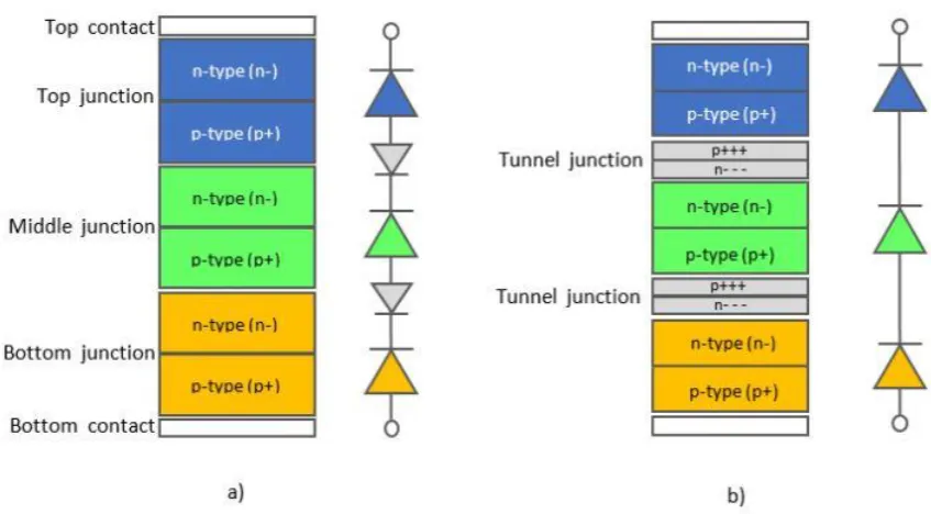
2.9. The multi-junction solar cell ... 30
2.10. MJSC architecture related modelling techniques ... 31
2.10.1. Production methods ... 31
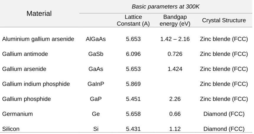
2.10.2. Semiconductor band gap energy and lattice constant ... 31
2.11. Loss mechanisms related to MJSC architecture ... 33
2.11.1. Tunnel junctions ... 34
2.12. Proven multi-junction solar cells ... 35
2.13. D1 and D2 MJSC equivalent circuits ... 36
2.14. Iterative changes to SJSC design for MJSC architecture ... 37
2.14.1. SJSC algorithm for parameter extraction in MJSCs... 37
2.14.2. Adapting the saturation current to the MJSC architecture ... 38
2.14.3. Simulink adjustments ... 39
2.14.4. Modelling conversion efficiency in MJSCs ... 42
2.14.5. Calculating total Voc... 42
2.15. Summary of characteristics ... 43
2.16. Summary of modelled expressions for MJSC simulation ... 44
Summary of literature review outcomes ... 45
Chapter 3:
Methodology ... 46
vii
3.1.1. Loading initial conditions (Step 1) ... 48
3.1.2. Extracting unknown parameters (Step 2) ... 48
3.1.3. Simulated Model forms (Step 3) ... 53
3.1.4. Collating simulation results for discussion (Step 4) ... 55
3.1.5. Validation and relative error percentage ... 56
3.2. Simulated single junction solar cells ... 57
3.2.1. Results of parameter extraction ... 57
3.3. Simulated multijunction solar cell ... 58
3.3.1. GaInP/GaInAs/Ge (D2) simulation ... 58
3.3.2. GaInP/GaInAs/Ge (D2) triple MJSC initial conditions... 58
Chapter 4:
Results and Analysis ... 60
4.1. Results of Kv form simulations ... 60
4.1.1. Kv form efficiency with respect to model accuracy ... 62
4.1.2. Kv form efficiency with respect to irradiance ... 62
4.1.3. Kv form efficiency with respect to temperature ... 65
4.2. Results of Eg form simulations ... 67
4.2.1. Eg form efficiency with respect to model accuracy ... 69
4.2.2. Eg form efficiency with respect to irradiance ... 69
4.2.3. Eg form efficiency with respect to temperature ... 72
4.3. GaInP/GaInAs/Ge simulation results ... 74
4.3.1. GaInP/GaInAs/Ge open circuit voltage characteristics ... 75
4.3.2. GaInP/GaInAs/Ge recombination characteristics ... 77
4.3.3. GaInP/GaInAs/Ge efficiency with respect to irradiance and temp. ... 77
Summary of SJSC and MJSC performance ... 80
Chapter 5:
Project conclusion ... 85
5.1. Summary of outcomes ... 85
5.2. Project research contribution ... 85
viii
List of references ... 88
Appendices ... 93
Appendix 1
Project Specification ... 94
Appendix 2
Project Plan Risk Assessment ... 95
Appendix 3
Project Plan Communication ... 96
Appendix 4
Project Plan Resources ... 97
Appendix 5
Project Plan Timeline ... 98
Appendix 6
MATLAB script - Initial conditions ... 99
Appendix 7
MATLAB script - D1 extraction ... 100
Appendix 8
MATLAB script - D2 extraction ... 101
Appendix 9
Simulink block model - D1_Eg ... 102
Appendix 10
Simulink D2_Eg block model ... 105
Appendix 11
Simulink D1_Kv block model ... 108
Appendix 12
Simulink D2_Kv block model ... 111
Appendix 13
MATLAB script
–
Tvar Data ... 114
Appendix 14
MATLAB script
–
Gvar Data... 117
Appendix 15
D1_Kv form and D2_Kv form data ... 120
Appendix 16
D1_Eg and D2_Eg data... 130
Appendix 17
Interpolation and plotting code ... 140
Appendix 18
Simulink D2 MJSC block model ... 147
Appendix 19
GaInP/GaInAs/Ge simulation results ... 151
ix
Table of Figures
Figure 1: Conventional single junction PV cell. Image from (Chin, Salam & Ishaque 2015). ... 3
Figure 2: Various representations of a P-N junction diode. ... 4
Figure 3: Atom showing three orbitals and their respective energies... 5
Figure 4: The electrons shells of a) several atoms, and b) countless atoms. ... 5
Figure 5: Material state bandgap energies. Image taken form (Mertens & Roth 2014). ... 6
Figure 6: Single diode equivalent circuit. ... 6
Figure 7: Diode curve characteristics Image from (Markvart & Castañer 2012) . ... 8
Figure 8: Characteristic curves of a solar cell diode. ... 9
Figure 9: The effect of changing Rs on the SJSC VI & VP curves. ...13
Figure 10: The effect of changing values of RP, on VI & VP characteristic curves. ...14
Figure 11: Early theoretical and experimental efficiencies. Image from (W. Shockley 1961). ...15
Figure 12: Spectrum utilisation of a 1.4ev bandgap. Image from (Tanabe 2009) ...16
Figure 13: PV cell bandgap. Image from (Mertens & Roth 2014) and (Chin, Salam & Ishaque 2015) ...17
Figure 14: Bandgap loss mechanisms. Image from (Foozieh Sohrabi 2013). ...18
Figure 15: Representative PV energy losses. Image from (McEvoy, Castaner & Markvart 2012). ...20
Figure 16: Single diode equivalent circuit ...21
Figure 17: Double diode equivalent circuit. ...24
Figure 18: Schematic representation of a MJSC. Image from (Friedman 2010). ...30
Figure 19: Bandgap as a function of lattice constant. Image taken from (Friedman 2011). ...32
Figure 20: MJSC without/with tunnel junctions. Image adapted from (Cotal et al. 2009). ...34
Figure 21: Double junction diode. Image taken from (Jain & Hudait 2012) ...35
Figure 22: Efficiencies of the GaInP/GaInP/Ge MJSC. Image taken from (King et al 2007). ...36
Figure 23: (Left) D1 MJSC equivalent circuit and (Right) D2 MJSC equivalent circuit. ...37
Figure 24: Simulink model of a triple junction solar cell. ...40
Figure 25: D2 Simulink model of a single cell junction. ...41
Figure 26: Simulink modelled MJSC junction saturation current. ...41
Figure 27: An example of the Simulink block environment. ...46
Figure 28: Flow chart outlining simulation process. ...47
Figure 29: MATLAB script 2 and 3 extraction algorithm flowchart. ...52
Figure 30: The D1_Kv output current (I) block build, as seen within the Simulink GUI. ...61
Figure 31: The D2_Kv output current (I) block build, as seen within the Simulink GUI. ...61
Figure 33: Comparison of D1_Kv and D2_Kv VP curves with respect to irradiance. ...63
Figure 33: Comparison of D1_Kv and D2_Kv efficiency, with respect to irradiance. ...63
Figure 34: Comparison of D1_Kv and D2_Kv VP plots with respect to temperature...65
Figure 35: Comparison of D1_Kv and D2_Kv efficiency, with respect to temperature. ...65
Figure 36: The D1_Eg output current (I) block build, as seen within the Simulink GUI. ...68
x
Figure 38: Comparison of D1_Eg and D2_Eg VP curves with respect to irradiance. ...70
Figure 39: Comparison of D1_Eg and D2_Eg efficiency, with respect to irradiance. ...70
Figure 40: Comparison of D1_Eg and D2_Eg VP curves, with respect to temperature. ...72
Figure 41: Comparison of D1_Eg and D2_Eg efficiency with respect to temperature. ...72
Figure 42: Approximation of spectral absorption at (500 & 1000)W/m2 ...75
Figure 43: GaInP/GaInAs/Ge VI characteristics at 500W/m2 and at 1000 W/m2 ...76
Figure 44: The VP characteristics of the GaInP/GaInAs/Ge (500 W) ...77
Figure 45: GaInP/GaInAs/Ge total cell VP characteristics with respect to irradiance. ...78
Figure 46: GaInP/GaInAs/Ge total conversion efficiency with respect to irradiance ...78
Figure 47: GaInP/GaInAs/Ge total VI curves with respect to irradiance. ...78
Figure 48: GaInP/GaInAs/Ge cell total efficiency at various Temperatures (˚C). ...79
xi
List of Tables
Table 1: Basic crystal structure parameters for commonly used MJSC semiconductors. ...33
Table 2: Dual MJSC InGaP/GaAs performance characteristics. ...35
Table 3: Analysis chart summarising parameter characteristics. ...43
Table 4: Equations required for MJSC D2 equivalent model. ...44
Table 5: Summary of equations within D1_Kv and D2_Kv models. ...53
Table 6: Summary of equations within D1_Eg and D2_Eg models. ...55
Table 7: Validation of D1 and D2 extracted parameters. ...57
Table 8: GaInP/GaInAs/Ge (Hussain et al. 2016) (D2) triple MJSC initial parameters ...58
Table 9: Initial conditions for the Kv form D1 and D2 models. ...60
Table 10: Relative MPP errors for D1_Kv and D2_Kv form models. ...62
Table 11: D1_Kv form model data for efficiency with respect to irradiance. ...64
Table 12: D2_Kv form model data for efficiency with respect to irradiance...64
Table 13: D1_Kv form model data of efficiency with respect to temperature. ...66
Table 14: D2_Kv form model data of efficiency with respect to temperature. ...67
Table 15: Initial conditions for the Eg form of D1 and D2 models. ...67
Table 16: Relative MPP errors for D1_Eg and D2_Eg form models. ...69
Table 17: D1_Eg form efficiency with respect to irradiance. ...71
Table 18: D2_Eg form efficiency with respect to irradiance. ...71
Table 19: D1_Eg form efficiency with respect to temperature...73
Table 20: D2_Eg form efficiency with respect to temperature...73
Table 21: GaInP/GaInAs/Ge simulation results at 0.5 suns, 40˚C. . ...74
Table 22: GaInP/GaInAs/Ge simulation results at 1 suns, 25˚C. ...74
Table 23: Summary of results for the Kv form models with respect to accuracy. ...80
Table 24: Summary of results for the Eg form models with respect to accuracy. ...81
Table 25: Summary of results for the Kv form of modelling with respect to efficiency. ...82
Table 26: Summary of results for the Eg form of modelling with respect to efficiency. ...83
xiii
Nomenclature
a ideality factor for the diffusion current component of diode (D1 model)
a1 ideality factor for the diffusion current component of diode 1 (D2 model)
a2 ideality factor for the rccombination current component of diode 2 (D2 model)
D1 Single diode model
D2 Double diode model
Eg bandgap energy (eV)
FF fill factor
Gc actual measured irradiance of the PV cell
Gstc reference irradiance under standard test conditions ( 1000 W/m2)
I total current that is generated by the cell, minus losses
Iph the photon generated current
Iph_stc photocurrent under STC conditions, and can be approximated by Isc_stc
IRS the voltage across the series resistances
Irs the recombination current, is used to determine the saturation current.
Is the diode saturation current for the D1 model - measured under reverse bias dark
conditions and usually referred to as the reverse saturation current, saturation
current or leakage current
Is1 the first diode dark/reverse saturation current for the D2 model - measured under
reverse bias dark conditions and usually referred to as the reverse saturation current,
saturation current or leakage current
Is2 the second diode saturation current for the D2 model - measured under reverse bias
dark conditions and usually referred to as the reverse saturation current, saturation
current or leakage current
Isc the short circuit current, or when voltage is zero
Isc_stc Isc measured under STC
J current density. When comparing the characteristics of a device, the current can be
xiv
k Boltzmann’s constant, 1.381*10(-23)
KI temperature coefficient for the short circuit current (mA / °K)
KV temperature coefficient for the open circuit voltage (mV / °K)
λ photon wavelength
λBG bandgap wavelength
MJSC multi-junction solar cell
Ns the number of cells in the PV cell module
Pe the sum of ideality factor a1 and ideality factor a2.
Pin input power (W)
VI curve Voltage current curve. Often denoted in the literature as IV curve
VP curve Voltage power curve. Often denoted in the literature as PV curve
Pmpp power at the maximum power point (W)
q the charge of an electron, 1.602*10(-19)
SJSC single junction solar cell
STC Standard test conditions ( Gstc = 1000 W/m2 and Tstc = 25°C)
V total voltage generated by each cell
VD voltage across the PV cell diode,
Voc_stc open current voltage measured under STC conditions
Vt the Temperature dependant voltage for Ns cells (at any temperature)
RP represents the shunt losses within the PV cell
RS represents the series losses within the PV cell
TC the actual measured temperature of the PV cell (°C)
1
Chapter 1:
Introduction
1.1. Context
The conventional single junction solar cell is made of two bands of oppositely charged
semiconductor materials separated by a third neutral band material. Photons of a particular
wavelength will permeate the solar cell to the lower positively charged band, and according to
Bohr’s Atomic Model, will collide into the band-atoms with such force that the atom-electrons are
excited (knocked free) from their valence.
In an ideal solar cell the electron is forced into the negatively charged conduction band to remain
separated from its valence hole by the neutral band. This process becomes useful when an external
conduction wire bridges the bands such that an electrical current is produced by the action of the
electron-hole pair recombination.
Multijunction solar cells (MJSCs) respond to a range of photon wavelengths and provide a greater
conversion efficiency. And as the production of MJSCs becomes more commonplace, iterative
design methodology will play a greater role in design, by enabling the adaption of proven SJSC
modelling practices to model conversion efficiency in MJSCs.
1.2. Problem Specification
The first problem is to determine how single junction solar cell (SJSC) conversion efficiency is
modelled in Simulink. A literature review will be conducted to investigate the differences between
single diode models and double diode models.
The second problem is to determine which of the SJSC modelling practices are more/less adaptable
when modelling conversion efficiency in MJSCs. A further literature review will be conducted to
propose an iterative Simulink model that will simulate the conversion efficiency of several proven
MJSCs.
1.3. Aim and objectives
The main aim of this dissertation was to provide a standardised D2 equivalent circuit model to the
conversion efficiency in MJSCs and to identify a range of existing SJSC modelling practices that
are more/less adaptable for simulating the conversion efficiency of MJSCs within the Simulink
2 The modelling techniques reviewed and tested in this paper aim to provide students and researchers
a set of criteria that will assist in designing a model to identify which multijunction semiconductor
materials convert photons to DC current more efficiently.
1.4. Dissertation Overview
Chapter 1 contains a brief introduction with regards to the project context, problem specifications
and project aims.
Chapter 2 contains a brief introduction to several topics including conventional SJSCs, P-N
junction diodes, bandgap energy models. A literature review of SJSC subjects include photodiode
characteristics, conventional solar cell characteristics and D1 and D2 models. A literature review of
MJSC subjects includes structures that influence modelling techniques, loss mechanisms related to
MJSCs and provides a chart to assist analysing SJSC and MJSC characteristics.
Chapter 3 contains the project methodology. A Simulink simulation method is proposed for
comparing the accuracy of D1 and D2 SJSCs with regards to conversion efficiency, and a Simulink
simulation method is proposed for modelling the conversion efficiency of MJSCs
Chapter 4 provides a discussion on the results of the comparative simulation between D1 and D2
SJSCs with regards to conversion efficiency and contains a discussion on the results of the MJSC
conversion efficiency simulations.
Chapter 5 contains the project conclusions and outlines the project outcomes, provides a discussion
on how the project findings can benefit research, reflections on the project and identifies areas of
3
Chapter 2:
Literature Review
Chapter 2 contains a brief introduction to several topics including conventional SJSCs, P-N
junction diodes, bandgap energy models. A literature review of SJSC subjects include photodiode
characteristics, conventional solar cell characteristics and D1 and D2 models. A literature review of
MJSC subjects includes structures that influence modelling techniques, loss mechanisms related to
MJSCs and provides a chart to assist analysing SJSC and MJSC characteristics.
Single junction solar cells (SJSC)
2.1. The conventional single junction silicon solar cell
When defined in a very broad context, a conventional silicon PV cell can be considered as a dual
semiconductor diode/device made of a continuous crystalline Silicon (Si) structure. The device
converts the sun’s light (irradiance) into energy, in the form of direct current (DC) (Chin, Salam &
Ishaque 2015).
Figure 1 shows one representation/model that succinctly encompasses the fundamental behaviour
of a single Si PV cell. A phenomenon, commonly termed the photoelectric effect, occurs within the
p-n junction, where sun light photons of a particular wavelength are absorbed into the PV cell
(Chin, Salam & Ishaque 2015), creating a forced reaction whereby an electron is excited from its
valence and allowed to flow as current through the external wire conductor.
Although Figure 1 provides a succinct overview of the conventional silicon PV cell, it lacks the
sophistication to describe the conversion efficiency limitations of the crystalline silicon PV
semiconductor material.
The modelling in this paper will be based on compact modelling where device characteristics are
described by measuring equivalent circuit models consisting of of lumped components.
4 In a single diode (D1) model, for example, photons are represented by a DC current source and the
bulk behaviour of the solar cell is represented by an ideal diode. The double diode (D2) model
allows for an extra layer of complexity, where the second diode represents the behaviour of the
solar cell depletion region, hence, there will be some discussion and research of atomic concepts.
However it is not within the scope of this paper to model the atomic concepts in detail. Physical
parameters such as cell thickness, junction thickness, and doping concentrations are ignored, and it
is assumed that bandgap energies are ideal and the characteristic behaviour is predictable.
Likewise, the modelling of atomic parameters such as carrier concentrations, diffusivity and
recombination rates are not within the scope of this paper, as the design considerations for such
related behaviour is generally represented by including a second diode to represent the solar cell
depletion region.
2.1.1.
The P-N junction diode
Most of the measurable characteristics of a solar cell can be explained by the characteristic
behaviours of a P-N junction diode and and its junction bandgap energy.
When the anode terminal of a P-N junction diode is connected to the positive terminal of a battery
and the cathode terminal is connected to ground, the diode is said to be forward biased will conduct
current to the battery ground. When the anode and cathode terminals are interchanged, the diode is
said to be reversed biased and will insulate the current from reaching ground
The forward and reverse control of current flow is due to the interaction between the applied
electric field of the battery and the built in electric field of the PN junction. When the potential
across the diode reaches 0.6 - 0.7V in forward bias, the applied field exceeds the built in field and
current flows. When the potential across the diode is in reverse bias, the applied field will then add
to the built in field and block the current.
5 The conventional solar cell utilises the very same P-N junction current control characteristic to
convert the suns photons to DC current and much of the observable behaviour in a PN junction and
PV solar cell, can be described by the bandgap energy model.
2.1.2.
Bandgap energy model
The bandgap model is a very useful tool when designing PV solar cells as it succinctly describes
the correlation between material selection and conduction potential. Figure 3 shows an atom with
orbiting electrons with specific energy levels, or shells, which are represented by discrete electron
volt (eV) energy lines.
The greater the electron distance from the nucleus – the higher its energy level. When several
atoms of the same element bond, the electron shells overlap and the electrons are shared between
the atoms and the energy levels are no longer discrete (Figure 4a).
There are countless atoms in solid materials and the effect is magnified so the many overlapping
electron energy levels start to spread and energy band ranges emerge (Figure 4b):
Figure 3: Atom showing three orbitals and their respective energies.
6 The the lower energy band, known as the valence band, is indicative of the range of
valence electron energies for that particular solid.
The the upper energy band, known as the conduction band, is indicative of electron energies required to induce electron conduction in that particular material.
The gap/distance between the two bands is indicative of the amount of photon energy required to force an electron from its valence energy state to – the conduction energy state.
Figure 5 denotes the energy difference between the upper band and lower band as WG. Electrons
within the valence shells of conduction materials require no extra energy to change from a valence
electron to a free electron. Electrons within the valence shells of insulation materials usually
require more than 3ev of energy to clear the bandgap, however this amount of energy would
severely compromise the material. Electrons within the valence shells of semiconductor materials
require anywhere in the range of 0 to 3ev to clear the bandgap.
It is the ability - to determine the which of the semiconductor materials provide a better conversion
response to a broader light spectrum - that makes it possible to design MJSCs with a higher
conversion efficiency.
2.2. The photodiode based solar cell model
Given that the solar cell is a photodiode device, then it makes sense that it can be characterised by a
diode based equivalent circuit model.
Figure 5: Material state bandgap energies. Image taken form (Mertens & Roth 2014).
7 The following parameters are contained within the equivalent circuit:
The current source (Iph) that represents the photoelectric effect due to sunlight;
An ideal diode (Vd) parallel to Iph, representing an ideal PV junction within the solar cell;
A parallel resistor (Rp) representing the shunt losses within the PV cell;
A series resistor (Rs) representing the series losses within the PV cell;
Total current (I), the current that is generated by the cell, minus losses;
Total voltage (V), the voltage across the load
As circuit theory dictates, equivalent circuit output current (I) will increase if the series resistance is
very low to nil and the parallel resistance is very high to infinity. Hence, the characteristic equation
for the single diode model, including shunt and series losses, is given by:
𝐼 = 𝐼𝑝ℎ− 𝐼𝑠(𝑒𝑥𝑝 ( 𝑉+𝐼𝑅𝑠
𝑎∙𝑉𝑡 ) − 1) − 𝑉+𝐼𝑅𝑠
𝑅𝑝 Equation 1
The photo current is represented by Iph, and the diode current is represented by the transient part of
the expression and its co-efficient Is, and the current due to resistances are represented by the
fraction/real part of the expression.
2.3. Ideal photodiode and characteristic curves
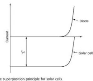
In 1961 William Shockley and Hans Queisser published a paper containing the derivation of an
ideal diode equation (W. Shockley 1961) which provides a means to predict the behaviour of a
diode by utilising its super positional qualities. When the diode is exposed to light the electron and
hole charges in the p-n junction are separated, generating a forward biased current
(González-Longatt 2005). The VI characteristics can be described by subtracting the short circuit current from
the ‘non illuminated’ ideal diode equation (Equation 2 on page 8), and although the diode is reverse
8 Figure 7 contains a diagram taken from (Markvart & Castañer 2012):
i. The characteristic of an ideal diode in the dark is represented by the top “Diode” curve;
ii. The characteristic of the diode when exposed to light is represented by the lower “Solar cell” curve;
Consider the single diode equivalent circuit shown in Equation 1, where Iph represents the current
generated under sunlight and Id is the current generated when there is no sunlight. Therefore the
total current, I, is simply the difference between the diode generated current under light and the
diode generated current in the dark (as the two currents flow in opposite directions) (Jha 2009).
The electrical characteristics of the source parallel diode is made up of a real current part and a
transient part. The transient/real relationship is more accurately described by William Shockley’s
ideal diode equation, where ID is the current through the diode:
𝐼𝐷 = 𝐼𝑠
(
𝑒𝑥𝑝 𝑞∙𝑉𝑑𝑎∙𝑘∙𝑇𝑐− 1
)
Equation 2Where: Is is the diode’s saturation current,
Vd is the diode voltage;
q is the charge of an electron, 1.602e-19;
Tc is the temperature in Kelvin;
k is Boltzmann’s constant, 1.381e-23 and
[image:23.595.225.375.80.210.2]a is a diode ideality constant/factor.
9 The saturation current will increase as temperature increases (Mertens & Roth 2014), however, the
magnitude will be less severe - depending on the quality of the materials within the solar cell. A
perfect diode with perfect materials will have an ideality constant (a) equal to 1, meaning that the
diode obeys the ideal diode equation perfectly and there is no unwanted electron-hole-pair
recombination. However some degree of unwanted recombination is inevitable (Alharbi & Kais
2015) and a silicon PV cell diode will typically have an ideality factor between 1.2 and 1.7.
The ideality factor is closely linked to the effect of temperature on a device, so that when a diode
with a higher ideality factor is exposed to a higher temperature - will ‘turn on’ faster.
2.3.1.
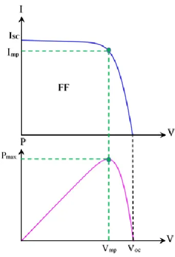
Solar cell characteristics
The characteristic curves of a solar cell very much follow photodiode characteristic curve
principles, however convention dictates that the diode characteristics shown in Figure 7 are to be
represented in the first quadrant being that the solar cell is producing power (Mertens & Roth
2014). The diagram in Figure 7. shows a negative current and a positive voltage, hence the current
axis is inverted in the Figure 8 diagram.
Much like the ideal diode characteristic curve, the characteristic equation (Equation 2) also applies
to the solar cell characteristic curves and allows for derivation of useful solar cell parameters. The
[image:24.595.234.405.398.649.2]following sub sections apply basic electrical analysis techniques to describe several important solar
10 cell parameters, the solar cell characteristic curves, and the solar cell characteristic equation
(Equation 2).
2.3.1.1
Short circuit current
Figure 8 shows that the short circuit current occurs when the solar cell is shorted, voltage is equal
to zero and the current is at its maximum value. Assuming that the solar cell is ideal, parallel
resistance is infinite and losses are ignored, then when the cell is shorted there is no current through
the diode (Figure 6) and it can be said that:
i. when the solar cell voltage equals zero, ISC equals Iph,
ii. and hence, ISC is proportional to irradiance.
Irradiance proportionality then provides some insight into semiconductor material selection with
respect to solar cell design and bandgap energy. The lower the energy of the semiconductor
bandgap, then the higher the solar cell efficiency will be (W. Shockley 1961), so it can be said that:
iii. lower bandgap energies absorb a greater quantity of photons,
iv. hence ISC increases as the energy of the bandgap decreases.
2.3.1.2
Open circuit voltage
Figure 8 shows on both axis’ that when solar cell current equals zero, the solar cell voltage is at its
maximum open circuit voltage (VOC). VOC can be found from the ideal form of Equation 3 by
setting I equals to zero, Iph equals ISC and solving for VOC:
Where: Vt is the temperature dependant voltage (V),
Isc is the the short circuit current (A),
and ISis the saturation current.
Area is the srface area of the solar cell (m),
The expression contains a natural logarithm, which indicates that the open circuit voltage is less
dependant on irradiance than the short circuit current is (Mertens & Roth 2014):
i. and hence, VOC is proportional to the natural log of irradiance.
𝑉𝑂𝐶= 𝑎 ∙ 𝑉𝑡∙ ln ( 𝐼𝑆𝐶
11 As with ISC, VOC is an interesting parameter in terms of bandgap material selection, as VOC is a
function of bandgap energy (W. Shockley 1961) and as such:
ii. VOC increases as bandgap energy increases,
iii. and as VOC increases, efficiency increases until the current starts to drop.
2.3.1.3
Fill factor and maximum power
The fill factor, denoted by FF in Figure 8, is a graphical tool that provides a ratio that represents the
quality of a power cell. Generally speaking, a less rounded VI characteristic curve will provide a
higher fill factor and represents a high quality solar cell. The fill factor is described by:
Where: Pmpp is the power at the maximum power point (W),
Vmpp is the maximum voltage (V),
Impp is the maximum current (A),
Voc is the the open current voltage (V),
Isc is the the short circuit current (A),
It is difficult to improve the fill factor of a poor quality cell, but it is not difficult to degrade the fill
factor of a good solar cell if the series resistance high - due device contacts. The FF can also be
approximated by the following expression (Mertens & Roth 2014):
𝐹𝐹 = 1+ln( 𝑉𝑂𝐶
𝑉𝑡+0.72) 𝑉𝑂𝐶
𝑉𝑡+1
Equation 5
Where: Vt is the temperature dependant voltage (V),
The maximum power point of a solar cell (Figure 8) is the point where the maximum current and
maximum voltage s graphically intersect to give the greatest fill factor area. 𝐹𝑖𝑙𝑙 𝐹𝑎𝑐𝑡𝑜𝑟 = 𝐹𝐹 = 𝑉𝑚𝑝𝑝 ∙ 𝐼𝑚𝑝𝑝
𝑉𝑂𝐶 ∙ 𝐼𝑆𝐶 =
𝑃𝑚𝑝𝑝
12
2.3.1.4
Efficiency
Solar cell efficiency provides a means to quantify the power output of a PV cell as a
percentage/ratio of the suns input (Tanvir Ahmad* March 2016). A cell with a low efficiency
requires a greater area to produce a given power, needs more natural resources and will have a
higher relative cost to manufacture compared to more efficient cell.
𝑆𝑖𝑛𝑔𝑙𝑒 𝑗𝑢𝑛𝑐𝑡𝑖𝑜𝑛 𝑐𝑒𝑙𝑙 𝑒𝑓𝑓𝑖𝑐𝑖𝑒𝑛𝑐𝑦 = 𝜂𝑆𝐽𝑆𝐶 = 𝑃𝑚𝑝𝑝
𝑃𝑖𝑛 =
𝑉𝑜𝑐∙𝐼𝑠𝑐∙𝐹𝐹
(𝐴𝑟𝑒𝑎(𝑚𝑚2)
1000 )
∙ 100
Equation 6
Where: Pin is the solar cell input power (W)
Pmpp is the power at the maximum power point (W),
Voc is the the open current voltage (V),
Isc is the the short circuit current (A),
FF is the fill factor,
Area is the surface area of the solar cell (m),
2.3.2.
Parasitic series resistance (
R
S) losses
The series resistance (Rs) primarily represents losses due to (1) current through the solar cell
emitter and base, (2) resistance within the metal contact material and (3) the resistance caused at
the interface between the metal contacts and the solar cell semiconductor materials.
Series resistance is normally considered to occur as a result of poor design and reduces the
characteristic fill factor. The effect of a changing series resistance on the characteristic VI and VP
13 Consider Figure 9 and note the following observations with respect to each graph:
The y-axis of the LHS graph represents the cells short circuit current (ISC),
The y-axis of the RHS graph represents the cells power (P),
The x-axis of each graph represents the cells open circuit cvoltage (VOC),
The series resistance has no effect on the cell short circuit current (ISC) or the cell open
circuit voltage (VOC).
The cell fill factor increases as the series resistance tends to zero,
A linear increase in resistance provides a generally linear reduction in the maximum power point (MPP).
2.3.3.
Parasitic shunt/parallel resistance (
R
P) losses
Losses due to shunt/parallel resistance is generally due to manufacturing defects, transportation
defects and damage due to careless installation.
Cracked or scratched cells provide an alternate current path, reducing the amount of current
flowing through the solar cell junction culminating in a lower voltage potential across the solar cell.
The effects of a changing shunt resistance on the characteristic VI and VP curves is shown in
Figure 10.
14 Consider Figure 10 and note the following observations with respect to each graph:
The y-axis of the LHS graph represents the cells short circuit current (ISC),
The y-axis of the RHS graph represents the cells power (P),
The x-axis of each graph represents the cells open circuit cvoltage (VOC),
Assuming that the series resistance is zero, then it can be said that the shunt resistance has no effect on the short circuit current (ISC).
However, the shunt resistance will reduce the cell’s open circuit voltage (VOC) as the shunt
approaches zero.
The cell fill factor increases as the shunt resistance tends to infinity,
A linear increase in resistance does not provide linear increase in the maximum power point (MPP), that is, lower values of shunt resistance leads to a much lower solar cell
conversion efficiency.
2.3.4.
The effect of temperature and irradiance
Temperature is a primary concern when designing for PV cell efficiency, as an increase in
temperature results in a marked loss in efficiency due to large losses in open circuit voltage, slight
increase in short circuit current - not withstanding.
An increase in irradiance is obviously beneficial to a solar cells output power, as the short circuit
current (ISC) will increase linearly as irradiance increases. However efficiency does not have a
linear response, as it is dependant on the inverse (log) voltage exponent shown in Equation 1. The
15 irradiance affects all parameters of the solar cell including ISC, VOC, the fill factor (FF), and both
forms of resistance. The effects of temperature and the effect of irradiance are discussed at length
in Chapter 3.2 of this report.
2.3.5.
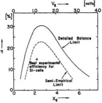
Inherent limitations for cell efficiency
Much of the advancement in new PV cell technology is driven by the limitations imposed on
existing technologies due to the theoretical limit for a materials conversion efficiency. In
Shockley’s 1961 paper, he discusses the theoretical limit for the (conversion) efficiency of p-n
junction PV cells and proves the upper obtainable efficiency for a single solar cell, with a single
material and a single bandgap to be 33%.
The upper obtainable efficiency for a single solar cell contained the following assumptions:
i. Only auger and band to band recombination occurs;
ii. All photons with energy greater than the bandgap are absorbed, and all electron hole pairs
have thermalisation loss;
iii. No losses occur when charge carriers are collected and transported.
The slowing rate of advancement in Si technology means that the return on investment in silicon
PV efficiency research will continue to diminish
It would appear that MJSCs may be able to circumvent this limitation by simply adding more
junctions, however, ultimate efficiency and the thermodynamic limit provides that as the number of
[image:30.595.199.363.421.587.2]junctions approach infinity, efficiency approaches zero.
16
2.3.6.
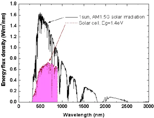
The solar spectrum
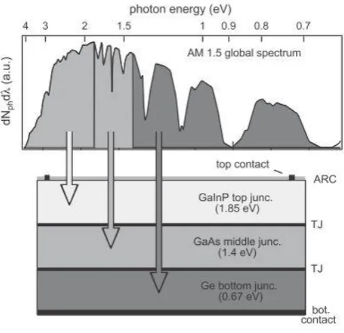
The solar spectrum is standardised to provide a reference for comparing conversion efficiencies
across all manner of PV cells and PV cell models. The AM1.5 global spectrum has been ratified for
non-concentrate models, and allows for a global mid latitude of 48.2 degrees to the normal
(equator).
The integrated power for the AM1.5 spectrum equates to 1000 watts per square metre, hence, a 1
cm2 solar cell with a conversion efficiency of 10% would produce 10 mW of power.
There are various atmospheric and detritus that will absorb the particular photon frequencies so that
the wavelengths are not recorded at ground level, and these can be observed in the spectrum as
dramatic drops in values of spectral irradiance, as seen by the indents in the Figure 12 AM1.5 solar
irradiation line.
2.4. The conventional silicon PV cell band gap
As previously discussed, the bandgap model provides a powerful tool when designing PV cells,
furthermore, the model characterises the inverse relationship between the wavelength of light and
[image:31.595.147.448.213.444.2]the energy of a photon. The sun provides a range of photon energies between approximately 0.4 to
17 3.1 eV, and the P-N junction bandgap of a Si PV cell can be considered as the level of the solar
spectrum, that the material absorbs most efficiently (Buonassisi 2013).
The diagram in Figure 13 is an amalgamation of two separate diagrams – taken from (Chin, Salam
& Ishaque 2015) and (Jha 2009). The conventional Si PV cell has been modified to show a more
detailed representation of the cell junction showing the bandgap that exists between the crystalline
N-type silicon (conduction band) and the crystalline P-type silicon (valence band) (Green 1982).
The energy band is commonly denoted by Eg, and is often referred to as the “band-gap” or the “forbidden layer/gap”.
Consider that the sunlight radiating onto the device injects a photon (of some wavelength) that
permeates the conduction band and band gap. The photon will be absorbed in the valence band at
some depth and an excitation reaction will occur at the absorption site where the energy of the
photon will generate an electron hole pair (Green 1982) within the valence band substrate.
Consider that a silicon atom in the valence band is struck by a photon of a particular length, the
photon will cause an electron to be knocked free from the atom with enough force to clear the the
band gap and settle within the conduction band (Figure 13). The result of the photon hole-pair
interaction provides a potential difference between the two bands across the energy gap, and
ideally, the only way for the electron-hole-pair to recombine is to flow (as current) through the
external conductor.
The photon requires a higher energy state than the p-n junction band gap to ensure that the
negatively charged electron will traverse the band gap to reside in the n-type band. It is then
[image:32.595.222.408.246.473.2]considered as a minority carrier (with respect to the negative-type (n-type) silicon) and the original
18 atom is considered to be a vacancy/hole that is analogous to a positively charged particle (Green
1982).
The Si PV cell p-n junction has an optimum bandgap energy (Eg) of approximately 1.12 electron
volts (eV). That is to say, that the p-type Si semi-conductor material will absorb photons with some
limited range of energy greater than 1.12 eV and any photons that are above or below this range are
considered wasted.
The bandgap energy property is not unique to only Si semiconductor materials and there are many
semiconductor materials that provide an optimum bandgap, for a range frequencies in the solar
spectrum. Alternative band-gap energies will be discussed further when discussing multi-junction
PV solar cells (MJSC).
2.4.1.
Bandgap related loss mechanisms
Parasitic resistance losses are discussed on page 12 of this report, however a closer review of
bandgap related loss mechanisms is warranted to provide a clearer understanding of why
recombination occurs and what mechanisms are to be considered with regards to lumped
recombination current (Irs) and to give some insight into recombination mechanisms involved in
multijunction cell design.
Examples of common loss mechanisms that occur in and around cell junctions between bandgaps
and photons , are represented in the Figure 14 diagram (Foozieh Sohrabi 2013).
Photons and bandgaps can be considered in terms of wavelength or energy so that:
When a bandgap is expressed in terms of energy it is denoted by Eg. The corresponding matching wavelength for that bandgap energy is denoted by λg;
19 When a photon is expressed in terms of wavelength it is denoted by λph. If that photon is
expressed in terms of energy, it is denoted by Eph.
The loss mechanisms represented in Figure 14, occur as a result of the following:
i. Transmission losses ( λph > λg ) ( Eph < Eg )
Optical losses encompass such losses as reflection, shading and transmission losses. The
bandgap wavelength (λg) is the wavelength of a photon that is most efficiently absorbed by
the semiconductor material of a single solar cell p-n junction (Mertens & Roth 2014).
Transmission loss occurs when the photon wavelength (λph) is greater than λg , hence the
photon will not have enough energy (Eph) to force an electron across the bandgap to the
conduction band. Transmission loss is illustrated by (1) in Figure 14, an image taken from
(Foozieh Sohrabi 2013).
ii. Thermalisation losses ( λph < λg ) ( Eg > Eph )
Thermalisation loss occurs when λph is less than λg and the Eph is greater than Eg.
Although the photon has successfully created an electron hole pair that remains separated
in the correct bands, there is excess energy loss to the lattice via phonons as heat energy
during thermal equalisation, as illustrated by (2) in Figure 14.
iii. Electrical and Ohmic losses
Electrical losses occur due to cell contact design; and ohmic losses can occur due to the
Schottky contact effect on any metal (plate) and semiconductor (material) interface
(Mertens & Roth 2014). The Schottky contact effect is illustrated by (3) and (4) in Figure
14, where the a p-n junction type mechanism occurs at the interface and reduces the overall
potential of the device.
iv. Recombination losses.
Recombination losses occur in the base, emitter and bandgap regions and usually via one
of three mechanisms:
a. Band to band (radiative) recombination where an electron from the conductance
band recombines with a hole in the valence band to release a photon. This is
illustrated by (5) in Figure 14;
b. Auger recombination where an electron from the conductance band recombines
with a hole in the valence band, however the collision produces another electron
(rather than a photon) that is released to the conductance band (McEvoy, Castaner
& Markvart 2012);
c. Shockley-Read-Hall recombination occurs in semiconductors that have been doped
20 within the bandgap due to a impure material defect, where it may recombine to
form a photon or a phonon (Sah, Noyce & Shockley 1957).
A graphical representation of the unavoidable and intrinsic losses that occur during energy
conversion in a single junction Si PV cell is shown in Figure 15, an image taken from (McEvoy,
Castaner & Markvart 2012).
Although the graph is not to scale, the energy verse current plot represents the losses from an ideal
Si cell with a bandgap of 1.12 eV that has been measured under standard test conditions. The losses
include:
Transmission losses, denoted by the ( hv < Eg ) shaded region, represent approximately 18.5% of the total losses;
Thermalisation losses, denoted by the ( hv > Eg ) shaded region, represent approximately 47% of the total losses;
[image:35.595.135.496.197.412.2] Recombination losses, denoted by the ( V < Eg ) shaded region; represent approximately 1.5% of the total losses;
21
2.5. The single diode (D1) model
As already discussed in this paper, the conventional single junction Si PV cell can be represented
by using the standard single single diode model, shown here in Figure 16.
For the single diode model SJSC, the assumption that there are no recombination losses within the
p-n junction insulation (depletion) region (Ishaque, Salam & Syafaruddin 2011), hence the ideality
constant (a) is modelled as unchanging in the transient part of the diode current. The value of a
diode’s ideality is somewhat empirical - and opinions vary on selecting an appropriate value –
however a value between 1.2 and 1.7 is acceptable in most cases (Villalva, Gazoli & Filho 2009).
Short circuit current (Isc), series and shunt resistances (Rs and Rp), saturation current (Is) and the
diode ideality factor, a, are the five parameters required for the single diode model. The cell is
analysed under the standard test conditions (STC) where solar a spectrum of AM1.5, irradiance of
1000 W/m2 and cell temperature of 25 degrees Celsius are provided (Hyvarinen & Karila 2003).
The characteristic equation for the single diode model is found by subtracting the diode current (ID)
and the shunt current (IRp) from the photoelectric current (Iph) to solve for the current through the
series resistance, or cell current output (I):
The first expression on the RHS of Equation 7 is for the photon generated current (Iph), which is
dependant on both irradiance and temperature and given by:
𝐼 = 𝐼𝑝ℎ− 𝐼𝐷− 𝐼𝑅𝑝 Equation 7
22 Where:: Isc is the short circuit current, or when voltage is zero,
KI is the temperature coefficient for the short circuit current (mA / °C),
obtained from the manufacturers datasheet,
Tc is the actual measured temperature of the PV cell (°C),
Tstc is the reference temperature under standard test conditions ( 25°C / 298°K),
Gc is the actual measured irradiance of the PV cell,
Gstc is the reference irradiance under standard test conditions ( 1000 W/m2);
The second expression in Equation 7 is the diode current (ID), and can be substituted with
Shockley’s ideal diode equation (Equation 2) and considered in terms of a PV cell:
𝐼𝐷 = 𝐼𝑠
(
𝑒𝑥𝑝 𝑞∙𝑉𝑑𝑎∙𝑘∙𝑇𝑐− 1
)
= 𝐼𝑠(
𝑒𝑥𝑝 𝑉+𝐼𝑅𝑠𝑎∙𝑉𝑡 − 1
)
Equation 9Where: Vd is the diode voltage,
q is the charge of an electron, 1.602*10(-19),
Tc is the temperature in Kelvin,
k is Boltzmann’s constant, 1.381 * 10(-23),
a is a diode ideality constant, where a =1 if the diode is perfectly efficient,
V is the total voltage generated by each cell,
IRS is the voltage across the series resistances.
The first new term in Equation 9 is the temperature dependant voltage, which is given by:
V𝑡= 𝑁𝑠∙𝑘∙𝑇𝑐
𝑞 Equation 10
𝐼𝑝ℎ =
[
𝐼𝑠𝑐_𝑆𝑇𝐶+ 𝐾𝐼(
𝑇𝑐− 𝑇𝑠𝑡𝑐)]
∙(
𝐺𝑐23 Where: Ns is the number of series connected cells per module.
The second new term in Equation 9 is the saturation current (Is), which can be derived depending
on the approach taken. This section of this paper will assume that Is is to include the bandgap
energy (Eg) in the expression for the saturation current, which is given by:
𝐼𝑠= 𝐼𝑟𝑠
(
𝑇𝑐𝑇𝑠𝑡𝑐
)
3
∙ 𝑒𝑥𝑝
((
𝑞∙𝐸𝑔𝑎∙𝑘
) (
1 𝑇𝑠𝑡𝑐−1
𝑇𝑐
))
Equation 11Irs is another new term – that represents recombination current:
Where: Isc_stc is short circuit current as measured under STC conditions,
Iph_stc is the photocurrent as measured under STC conditions,
(approximated by Isc_stc),
Voc_stc is the open current voltage measured under STC conditions, a is the diode ideality factor, and
Vtstc is the temperature dependant voltage for Ns cells under STC conditions.
Note that the inclusion of Irs in the saturation current (Is) effectively computes the saturation
current twice to eliminate the diode diffusion factor (Bellia, Youcef & Fatima 2014).
Therefore, the single diode (D1) model of the output current of a PV cell module, is given by: 𝐼𝑟𝑠 =
𝐼𝑝ℎ_𝑠𝑡𝑐
𝑒𝑥𝑝( 𝑉𝑜𝑐_𝑠𝑡𝑐
𝑎∙𝑉𝑡𝑠𝑡𝑐)−1
= 𝐼𝑠𝑐_𝑠𝑡𝑐
𝑒𝑥𝑝( 𝑉𝑜𝑐_𝑠𝑡𝑐
𝑎∙𝑉𝑡𝑠𝑡𝑐)−1 Equation 12
𝐼 = 𝐼𝑝ℎ− 𝐼𝑠[exp (
𝑞(V+I∙𝑅𝑠)
𝑎∙𝑁𝑠∙k∙𝑇𝑐 ) − 1] − 𝑉+𝐼∙𝑅𝑠
𝑅𝑝
= 𝐼𝑝ℎ− 𝐼𝑠[exp ( V+I∙𝑅𝑠
𝑎∙V𝑡 ) − 1] −
𝑉+𝐼∙𝑅𝑠
24
2.6. The double diode (D2) model
Although the single diode model is arguably the most popular PV model, its accuracy diminishes at
lower voltages and lower irradiances (Chin, Salam & Ishaque 2015). The double diode (D2) model
includes a second diode that allows for the losses that occur during recombination in the depletion
region (Mahmoud et al. 2012).
The saturation current in the second diode is generally accepted as being equal to the first diode
saturation current, however the ideality factor varies, as the ideality factor is really a function of
voltage across the device. The first diode is often allocated an a1 of 1, and the second diode will
have an a2 equal or greater than 1.2 (Ishaque 2011) and (Mahmoud et al. 2012).
The derivation of the D2 model relationships are simply an extension of the D1 relationships. The
characteristic equation for the double diode model is found by subtracting the both diode currents
(Id1 and Id2) and shunt current from the photoelectric current to solve for the current through the
series resistance:
𝐼 = 𝐼𝑝ℎ− (𝐼𝑑1+ 𝐼𝑑2) − 𝐼𝑅𝑝 Equation 15
Sub in the ideal diode current and use the voltage divider rule to find the current through the shunt,
hence providing expression for the PV cell characteristic equation. Hence, the double diode (D2)
model of the output current of a PV cell module, is given by:
𝐼𝑝ℎ−
(
𝐼𝑑1+ 𝐼𝑑2)
− 𝐼𝑅𝑝− 𝐼 = 0 Equation 1425 𝐼 = 𝐼𝑝ℎ− 𝐼𝑠1[exp (
𝑞(V+I∙𝑅𝑠)
𝑎1∙𝑁𝑠∙k∙𝑇𝑐 ) − 1] − 𝐼𝑠2[exp (
𝑞(V+I∙𝑅𝑠)
𝑎2∙𝑁𝑠∙k∙𝑇𝑐 ) − 1] − 𝑉+𝐼∙𝑅𝑠
𝑅𝑝
𝐼 = 𝐼𝑝ℎ− 𝐼𝑠1[exp ( V+I∙𝑅𝑠
𝑎1∙𝑉𝑡 ) − 1] − 𝐼𝑠2[exp (
V+I∙𝑅𝑠
𝑎2∙𝑉𝑡 ) − 1] −
𝑉+𝐼∙𝑅𝑠
𝑅𝑝 Equation 16
Where: Iph is the photon generated current,
Is1 is the first diode saturation current,
Is2 is the second diode saturation current,
q is the charge of an electron, 1.602*10^(-19),
V is the total voltage generated by each cell,
IRS is the voltage across the series resistances,
a1 is the first diode ideality factor,
a2 is the second diode ideality factor,
NS is the number of cells in the PV cell module,
k is Boltzmann’s constant, 1.381 * 10^(-23),
TC is the actual measured temperature of the PV cell (°C),
RP represents the shunt losses within the PV cell,
Vtc is the Temperature dependant voltage for Ns cells (at any temperature).
The photocurrent and temperature dependant voltage expressions are identical to the D1 model, and
the saturation currents vary - only in quantity - to allow for the number of diodes and respective
ideality factors.
Hence, the D2 saturation currents are given by:
𝐼𝑠1= 𝐼𝑟𝑠1 ( 𝑇𝑐 𝑇𝑠𝑡𝑐)
3
∙ 𝑒𝑥𝑝 ((𝑞∙𝐸𝑎1∙𝑘𝑔) ( 𝑇1 𝑠𝑡𝑐−
1 𝑇𝑐))
𝐼𝑠2= 𝐼𝑟𝑠2 ( 𝑇𝑐
𝑇𝑠𝑡𝑐)
3
∙ 𝑒𝑥𝑝 ((𝑞∙𝐸𝑔
𝑎2∙𝑘) ( 1 𝑇𝑠𝑡𝑐−
1
𝑇𝑐)) Equation 17
26 𝐼𝑟𝑠1= 𝐼𝑝ℎ_𝑠𝑡𝑐
exp( 𝑉𝑜𝑐_𝑠𝑡𝑐
𝑎1∙𝑉𝑡)−1
= 𝐼𝑠𝑐_𝑠𝑡𝑐
exp( 𝑉𝑜𝑐_𝑠𝑡𝑐
𝑎1∙ 𝑁𝑠∙𝑘∙𝑇𝑐𝑞 )−1
𝐼𝑟𝑠2= 𝐼𝑝ℎ_𝑠𝑡𝑐
exp( 𝑉𝑜𝑐_𝑠𝑡𝑐
𝑎2∙𝑉𝑡 )−1
= 𝐼𝑠𝑐_𝑠𝑡𝑐
exp( 𝑉𝑜𝑐_𝑠𝑡𝑐
𝑎2∙ 𝑁𝑠∙𝑘∙𝑇𝑐𝑞 )−1
Equation 18
2.7. Alternative approaches to modelling diode saturation current
There are many considerations when determining appropriate modelling techniques for
conventional Si PV cells. There is a large body of work dedicated to extracting modelling
parameters to provide accurate estimation, however, there is no systematic documentation within
the literature, so a comprehensive and accurate benchmarking system is not yet available (Chin,
Salam & Ishaque 2015).
Whilst conducting the literature review, the modelling techniques were tested against expected
characteristics and results did not always correlate between similar papers. On further review it
became apparent that there are two distinct and predominant forms of translational equations when
calculating the saturation current.
2.7.1.
The Kv form saturation current.
The first predominant approach to modelling saturation current will be referred to as the Kv form
of modelling. The Kv form is important to this dissertation as it is the form that is used when
modelling the validation data. Features include:
a. The Kv form of saturation current modelling is used in papers such as (Ishaque
2011), (Ishaque, Salam & Syafaruddin 2011), (Ishaque, Salam & Taheri 2011) and
(Jena & Ramana 2015);
b. This form uses an alternative computational method that simplifies the saturation
current equation and incorporates the recombination current into the primary
equation for saturation;
c. The bandgap energy is ignored when modelling the saturation current of the
device;
d. The saturation current also includes a coefficient of voltage per Kelvin that does
not commonly appear in the alternative predominate approach.
e. The single diode (D1) model in the Kv form will be referred to as the D1_Kv
27
f. The double diode (D2) model in the Kv form will be referred to as the D2_Kv
model.
In the D1_Kv model - saturation current is given by Equation 19:
𝐼𝑠=
𝐼𝑠𝑐_𝑠𝑡𝑐+𝐾𝐼∙(𝑇𝑐−𝑇𝑠𝑡𝑐)
[exp(𝑉𝑜𝑐_𝑠𝑡𝑐+𝐾𝑣∙(𝑇𝑐−𝑇𝑠𝑡𝑐)
𝑎∙𝑉𝑡 )−1]
= 𝐼𝑠𝑐_𝑠𝑡𝑐+𝐾𝐼∙(𝑇𝑐−𝑇𝑠𝑡𝑐)
[exp(𝑉𝑜𝑐_𝑠𝑡𝑐+𝐾𝑣∙(𝑇𝑐−𝑇𝑠𝑡𝑐)
𝑎∙𝑁𝑠∙𝑘∙𝑇𝑐𝑞
)−1] Equation 19
Where: KI is the temperature coefficient for the short circuit current (mA / °K),
KV is the temperature coefficient for the open circuit voltage (mV / °K),
a is the ideality factor of the diode, which is found analytically to be between
1.2 and 2.0.
In the D2_Kv model, the saturation current is given by Equation 20:
𝐼𝑠1 = 𝐼𝑠2 =
𝐼𝑠𝑐_𝑠𝑡𝑐+𝐾𝐼∙(𝑇𝑐−𝑇𝑠𝑡𝑐)
[exp(𝑉𝑜𝑐_𝑠𝑡𝑐+𝐾𝑣∙(𝑇𝑐−𝑇𝑠𝑡𝑐) (𝑎1+𝑎2
𝑃𝑒 )∙𝑉𝑡𝑐
)−1]
= 𝐼𝑠𝑐_𝑠𝑡𝑐+𝐾𝐼∙(𝑇𝑐−𝑇𝑠𝑡𝑐)
[exp(𝑉𝑜𝑐_𝑠𝑡𝑐+𝐾𝑣∙(𝑇𝑐−𝑇𝑠𝑡𝑐) (𝑎1+𝑎2
𝑃𝑒 )∙𝑁𝑠∙𝑘∙𝑇𝑐𝑞
)−1] Equation 20
Where : a1, is the ideality factor of diode 1 is assumed to be unity,
a2, is the ideality factor of diode 2 is assumed to be two,
Pe is the sum of a1 and a2.
The D2_Kv model gives both saturation currents equal magnitude to remove the need for
computational iteration, and a1 is assumed to be unity whilst a2 is assumed to be any value up to
1.7, and somewhat flexible above a value of 1.2 (Ishaque 2011).
2.7.2.
The Eg form saturation current
The second predominant approach to modelling saturation current will be referred to as the Eg
form of modelling. The Eg form is important to this dissertation as it is the form that is used
required when modelling solar cells with multiple junctions.. Features include:
a. The Eg form of saturation current modelling is used in such papers as (Das,
Wongsodihardjo & Islam 2013), (Das, Wongsodihardjo & Islam 2015), (Lineykin,
28
b. This form of saturation current derivation implements translational that include the
bandgap energy of the device within the expression for the saturation current.
c. The single diode (D1) model in the Eg form will be referred to as the D1_Eg
model.
d. The double diode (D2) model in the Eg form will be referred to as the D2_Eg
model.
In the D1_Eg model – saturation current is given by Equation 11, first introduced on page 23:
𝐼𝑠= 𝐼𝑟𝑠
(
𝑇𝑐𝑇𝑠𝑡𝑐
)
3∙ 𝑒𝑥𝑝
((
𝑞∙𝐸𝑔𝑎∙𝑘
) (
1 𝑇𝑠𝑡𝑐−1 𝑇𝑐
))
In the D2_Eg model – saturation current is given by Equation 17, first introduced on page 25:
𝐼𝑠1= 𝐼𝑟𝑠1 ( 𝑇𝑐
𝑇𝑠𝑡𝑐)
3
∙ 𝑒𝑥𝑝 ((𝑞∙𝐸𝑔
𝑎1∙𝑘) ( 1 𝑇𝑠𝑡𝑐−
1 𝑇𝑐))
𝐼𝑠2= 𝐼𝑟𝑠2 ( 𝑇𝑐
𝑇𝑠𝑡𝑐)
3
∙ 𝑒𝑥𝑝 ((𝑞∙𝐸𝑔
𝑎2∙𝑘) ( 1 𝑇𝑠𝑡𝑐−
1 𝑇𝑐))
2.7.3.
Exponential coefficient for parasitic resistances
Another modelling technique that did not correlate with the literature when tested against expected
characteristics, was the use of an exponential coefficient for parasitic resistances. Eg form models
appeared to respond more accurately when RS(T) and RP(T) were multiplied by an exponential to
the value of negative KV, the coefficient of temperature.
This modelling technique is found in the associated documentation for the single solar cell library
block within Simulink (MathWorks 2015).
The temperature dependant resistances are given in the D1_Eg and D2_Eg models by:
𝑅𝑃
(
T)
= 𝑅𝑃(
𝑇𝑐𝑇𝑠𝑡𝑐
)
− 𝐾𝑉
29 𝑅𝑆
(
T)
= 𝑅𝑆(
𝑇𝑐
𝑇𝑠𝑡𝑐
)
− 𝐾𝑉Equation 22
Where: Rp is the extracted value for shunt resistance,
Rs is the extracted value for series resistance and
Kv is the voltage coefficient of temperature given in the manufacturer data
sheet.
The temperature dependant resistances are given in the D1_Kv and D2_Kv models by:
𝑅𝑃
(
T)
= 𝑅𝑃(
𝑇𝑐𝑇𝑠𝑡𝑐
)
0
Equation 23
𝑅𝑆
(
T)
= 𝑅𝑆(
𝑇𝑐𝑇𝑠𝑡𝑐
)
0Equation 24
Where: Rp is the extracted value for shunt resistance, and
Rs is the extracted value for series resistance.
The zero exponent in Equation 23 and Equation 24 effectively cancels the exponent, as the Kv
form has Kv included in Equation 19 for the D1 model and in Equation 20 for the D2 model.
2.8. Cells and modules
PV module voltage is determined by the number of series connected solar cells, PV current from
the module is dependant on the size and efficiency of the solar cells. In this paper, the
nomenclature for a number of series connected cells is Ns, and the nomenclature for a number of
parallel connected cells is Np. Therefore the calculations for current will take the number of
parallel cells into account, and the calculations for voltage will take the number of series cells into
account:
Total short circuit current = (ISC)(NP),
Total short circuit current at the maximum power point = (I