DEVELOPMENT OF INTEGRETED RF RECTIFIER AND POWER STORAGE FOR PORTABLE CHARGING SYSTEM
VICTOR JOSEPH
This Report is submitted in Partial Fulfillment of Requirement for Award of Bachelor of Electronic Engineering (Telecommunication Electronics) With Honors
Faculty of Electronics and Computer Engineering Universiti Teknikal Malaysia Melaka
II
UNIVERSTI TEKNIKAL MALAYSIA MELAKA FAKULTI KEJURUTERAAN ELEKTRONIK DAN KEJURUTERAAN
KOMPUTER
BORANG PENGESAHAN STATUS LAPORAN
PROJEK SARJANA MUDA II
Tajuk Projek : DEVELOPMENT OF INTEGRATED RF RECTIFIER AND POWER STORAGE FOR PORTABLE CHARGING SYSTEM Sesi
Pengajian : 1 6 / 1 7
Saya VICTOR JOSEPH
mengaku membenarkan Laporan Projek Sarjana Muda ini disimpan di Perpustakaan dengan syarat-syarat kegunaan seperti berikut:
1. Laporan adalah hak milik Universiti Teknikal Malaysia Melaka.
2. Perpustakaan dibenarkan membuat salinan untuk tujuan pengajian sahaja.
3. Perpustakaan dibenarkan membuat salinan laporan ini sebagai bahan pertukaran antara institusi pengajian tinggi.
4. Sila tandakan ( √ ) :
SULIT* *(Mengandungi maklumat yang berdarjah keselamatan atau kepentingan Malaysia seperti yang termaktub di dalam AKTA RAHSIA RASMI 1972)
TERHAD** **(Mengandungi maklumat terhad yang telah ditentukan oleh organisasi/badan di mana penyelidikan dijalankan)
TIDAK TERHAD
Disahkan oleh:
__________________________ ___________________________________
(TANDATANGAN PENULIS) (COP DAN TANDATANGAN PENYELIA)
Tarikh: ……….. Tarikh: ………..
III
“I hereby declare that this report is the result of my own work except for quotes as cited in the references”
Signature:
Author : Victor Joseph
IV
“I hereby declare that I have read this report and in my opinion, this report is sufficient in terms of the scope and quality for the award of Bachelor of Electronic Engineering
(Telecommunication Electronics) With Honors”
Signature :
Supervisor’s Name : Assoc. Professor Dr. Zahriladha Bin Zakaria
V
DEDICATION
VI
ACKNOWLEDGEMENT
VII
ABSTRACT
VIII
ABSTRAK
IX
TABLE OF CONTENT
CHAPTER TITLE PAGE TITLE OF PROJECT
STATUS REPORT FORM II STUDENT DECLARATION III SUPERVISOR DECLARATION IV
DEDICATION V
ACKNOWLEDGEMENT VI
ABSTRACT VII
ABSTRAK VIII
TABLE OF CONTENT IX
LIST OF TABLE XIII
LIST OF FIGURES XIV
LIST OF ABREVIATIONS XVI
X
1 INTRODUCTION 1
1.1 Research Background 1
1.2 Problem Statement 3
1.3 Objective 3
1.4 Scope of work 4
1.5 Project planning 5
1.6 Thesis organization 6
2 LITERATURE REVIEW 7
2.1 Introduction 7
2.2 Rf energy harvaster characterisation 8
2.3 Effeciency 9
2.4 Conventional rectifier 10
2.5 Topologies of rf energy harvesting 11
2.6 Diode specification for rectification 13
2.7 Impedancce matching network 14
2.8 Resistor as a load 15
2.9 Rf energy harvesting circuitary losses 16
2.9.1 Diode treshold voltage 16
2.9.2 Impedance matching losses 17
2.10 Summary of literature review 17
XI
3.1 Introduction 21
3.2 Pre-design of rectifier circuit using lumped element 22
3.3 Lumped element to microstrip line 23
3.3.1 Interdigital capacitor 24
3.4 Resistor analysis 26
3.5 Diode analysis 27
3.6 Matching netork analysis 28
3.7 Tuning and optimization 29
3.8 Dc step up-converter 30
3.8.1 Usb dc converter 30
3.8.2 Xl-6009 dc converter 31
3.8.3 Ltc3105 energy harvesting module 33
3.9 Storage device 34
3.10 Design layout 35
3.11 Fabrication process 37
3.12 Soldering process 38
3.13 Measurement process 39
3.14 Methodology work flow 42
4 RESULT AND DISCUSSION 43
4.1 Introduction 43
4.2 Rectifier design specification 44
4.3 Diode analysis 45
4.4 Resistor analysis 46
4.5 Result of matching network analysis 47
4.6 Simulation and measurement result 49
4.6.1 Schematic, momentum and lab measurement result. 50
XII
4.8 Analysis of dc converters and power storage 53
4.8.1 Usb dc converter analysis 53
4.8.2 Xl-6009 dc converter analysis 54
4.8.3 Ltc3105 energy harvesting module 54
4.8.4 Power storage analysis 55
4.9 Discussion 55
4.9.1 Comparisons of previous study 56
5 CONCLUSION AND SUGGESTION 58
5.1 Conclusion 58
5.2 Suggestion 61
5.2.1 Multiband operation 61
5.2.2 Apply the design in different material 62
5.2.3 Modifying rectifier topologies 62
REFERENCES 63
XIII
LIST OF TABLE
NO TITLE PAGE
1.1 Project Gantt-chart 5
2.1 Critical literature review 17
3.1 Interdigital capacitor parameters 25
3.2 Type of Schottky diode that will be analyze 27
3.3 Specification for the USB converter 30
3.4 Specification of XL-6009 DC converter 32
3.5 LTC3105 specification 33
3.6 Storage device specification and features 34
4.1 Rectifier specification 44
4.2 Measurement and simulation result 50
4.3 Analysis of USB DC converter 53
4.4 XL-6009 analysis 54
4.5 Analysis of LTC3105 energy harvesting 54
4.6 Power storage analysis 55
4.7 Comparisons of previous study with the proposed design 56
5.1 STM32L0 specification 59
XIV
LIST OF FIGURES
NO TITLE PAGE
1.1 RF energy harvesting system block 2
2.1 Conventional RF rectifier schematic diagram [2] 10
2.2 Cascaded rectifier [12] 12
2.3 Various topologies of RF rectifier [13] 12
2.4 The equivalent circuit for Schottky diode [15] 13
2.5 Illustration of matching network [1] 14
2.6 comparisons between a different values of RL over rectifier output 15 2.7 Relationship between efficiency and losses in RF energy harvesting 16
3.1 Pre-design of rectifier circuit. 22
3.2 Embedded micro-strip cross section 23
3.3 Inter-digital capacitor dimension and geometry 24 3.4 Interdigital capacitor in rectifier circuit 25
3.5 Resistor value analysis 26
3.6 Single stub matching 28
3.7 Double stub matching network 28
3.8 Tuning layout in ADS 2011 29
3.9 USB DC converter 31
3.10 Schematic circuit for the USB DC converter 31
3.11 XL-6009 DC converter 32
XV
3.13 Schematic diagram of the DC converter 33
3.14 Energy harvesting module 34
3.15 Storage device 35
3.16 Schematic circuit for the final rectifier design 36 3.17 EM layout of the complete rectifier circuit 36
3.18 Rectifier design in CORELDRAW 37
3.19 Fabricated rectifier design on FR4 board 38
3.20 Components soldered on FR4 board 39
3.21 Block diagram of the measurement process 40
3.22 RF Generator 40
3.23 In-Lab measurement process 41
3.24 Project flow chart 42
4.1 Analysis of different type of diodes 45
4.2 Analysis of different value of resistor 46
4.3 Result of matching network analysis 47
4.4 Resonant frequency of the matching network 48 4.5 Comparisons simulation result between schematic and momentum circuit.49
4.6 Graph of result comparisons 51
5.1 STM32L0 (ARM® Cortex®-M0+) Microcontroller 59
5.2 STTS751Temperature Sensors 60
5.3 Multi-band proposed rectifier 61
XVI
LIST OF ABREVIATIONS
RF - Radio Frequency
RFID - Radio Frequency Identification DC - Direct Current
ADS - Advance Design System
GSM - Global System for Mobile Communication ISM - Industrial, Scientific and Medical
SPICE - Simulation Program with Integrated Circuit Emphasis UTMS - Universal Mobile Telecommunications System WIFI - Wireless Fidelity
UHF - Ultra High Frequency
TEM - Transverse Electromagnetic Mode EM - Electromagnetic
XVII
LIST OF APPENDIX
APPENDIX A - HSMS 286X DIODE SPECIFICATION
APPENDIX B - XL-6009 DC CONVERTER SPECIFICATION APPENDIX C - LTC3105 SPECIFICATION
CHAPTER 1
INTRODUCTION
1.1 RESEARCH BACKGROUND
2
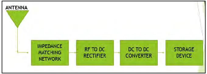
[image:20.612.157.497.384.506.2]Increased due to the development in broadcasting and wireless communication system. Moreover, the development of a mobile electronic devices, wireless implant healthy monitoring [2],micro-sensor and RFID system to operate without a batteries has triggered an intention for RF energy harvesting. Scavenging microwaves energy from an ambient environment and rectify to obtain a DC power wirelessly through a wireless transmission has been the issue of a research for decades. The concept of RF energy harvesting use the idea of scavenging a transmitted RF energy from an ambient environment then convert it into a DC signal to power up circuit or storing it for a future use[3]. Mainly, the conventional RF to DC converter consist of a few parts including antenna, input matching circuit, rectifier, output matching circuit and a load [4]. The antenna will capture the electromagnetic radiation and the matching circuit will optimizing the power delivered upon the RF energy extraction then the rectifier will rectify and convert those extracted signal into DC signal [3] via rectifying element as illustrated in figure 1.
Figure 1.1: RF energy harvesting system block
3
1.2PROBLEM STATEMENT
Laterally, a rapid growing on an advancement of a wireless technology has brought an intimation of transmitting power wirelessly as one of the solution to replace a power cord and a battery needs to power up a variety of an electronic devices. Traditionally, most of an electronic devices are attached by wires or powered by batteries which causing a user’s flexibility issues such as an electronic devices that attached with wire and a wireless devices which is powered by only a batteries that required to be charged periodically making the system less autonomous. Hench, as the energy is an essential requirement in all system, an environment friendly approach provides an opportunity to harvest the microwave signal from an ambient environment that commonly known as a RF energy harvesting. The existing design of a rectifier DC conversion that has been proposed in many research facing an issues of getting low output power as the energy captured from RF ambient source is low due to the effect of mismatching problem between antenna and rectifier. Moreover, even there is less issues of matching problem between an antenna and the rectifier, some problem as unstable voltage output is another concern to acquire clean DC output due to the changes of RF input power behaviour. Thus, in this project, an ideal design of a DC conversion of RF rectification is proposed together with an addition of a storage device as to deal with the unstable power output issues.
1.3OBJECTIVE
4
1.4SCOPE OF WORK
5
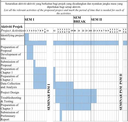
1.5PROJECT PLANNING
[image:23.612.121.534.285.678.2]The Gantt chart in table 1 shows the work flow that need to be done according to the time established. The Gantt chart helps to guide and complete each task on time.
Table 1.1: Project Gantt-chart
A. PERANCANGAN PROJEK
PROJECT PLANNING (GANTT CHART)
Senaraikan aktiviti-aktiviti yang berkaitan bagi projek yang dicadangkan dan nyatakan jangka masa yang diperlukan bagi setiap aktiviti.
List all the relevant activities of the proposed project and mark the period of time that is needed for each of the activities.
SEM I SEM BREAK SEM II
Aktiviti Projek
Project Activities 1 2 3 4 5 6 7 8 9 10 11 12 1
3 14 15 16 17 18 19 20 21 22 23 24 1 2 3 4 5 6 7 8 9 10 11 12 13 14 15 16 Identifying project title SE MI N A R PS M I SE MI N A R PS
M PSM
6