White Rose Research Online
eprints@whiterose.ac.uk
Universities of Leeds, Sheffield and York
http://eprints.whiterose.ac.uk/
This is the author’s version of an article published in
Physical Review B
White Rose Research Online URL for this paper:
http://eprints.whiterose.ac.uk/id/eprint/75643
Published article:
Califano, M and Zunger, A (2004)
Anisotropy of interband transitions in InAs
quantum wires: an atomistic theory.
Physical Review B (Condensed Matter), 70
(16). 1 - 11 . ISSN 0163-1829
Marco Califano and Alex Zunger
National Renewable Energy Laboratory, Golden, CO, 80401
The electronic and optical properties of [001]-oriented free-standing InAs cylindrical quantum wires (QWRs) with diameters 10–100 ˚A are calculated using an atomistic, empirical pseudopotential plane-wave method. We analyze the effect of different degrees of mixing between valence bands on the optical properties of these nanostructures, by switching on and off the spin-orbit interaction. The fundamental transition in these QWRs exhibit a large anisotropy, with emission polarized prevalently along the wire axisz. The magnitude of such an anisotropy is found to depend on both degree of valence band mixing and wire size. In higher energy interband transitions, we find anisotropies close to 100% with emission polarized perpendicular to the wire axis. Furthermore, in large wires, transitions involving highly excited valence states show in-plane polarization anisotropies between the [110] and [1¯10] directions. InAs wires can therefore switch betweenz-polarized toxy-polarized emission/absorption for different excitation energies. This makes them ideally suited for application in orientation-sensitive devices.
PACS numbers: 71.15.-m, 71.55.-i
I. INTRODUCTION
Recent advances in fabrication techniques such as laser assisted catalytic growth (LCG) and its variations, made it possible1-9 to produce high quality quantum wires (QWRs) of many III-V (InAs, InP, GaAs, GaP, GaN, etc), II-VI (ZnS, ZnSe, CdS, CdSe), and IV-IV (alloys of SiGe) semiconductors, with diameters ranging from 3 nm to several tens of nm, and lengths exceeding 1 µm. This growth method exploits laser ablation to gener-ate nanometer diameter catalytic clusters that define the size and direct the growth of the crystalline nanowires by a vapor-liquid-solid mechanism. The availability of such perfect cylindrical samples at a crystalline level of-fers challenging opportunities to the theorist to explain their properties and predict new features that can be exploited for the realization of novel devices. One of the most important properties of QWRs is the polar-ization anisotropy of their interband transitions: due to the 1D confinement, the emission/absorption intensity Ikfor light polarized parallel to the wire axis (z) can be different from that (I⊥) for light polarized in the (x, y) plane, perpendicular to it. The polarization anisotropy is defined in terms of the degree of linear polarization
ρ=αk−α⊥
αk+α⊥. (1)
whereαis the absorption coefficient. Furthermore, as the underlying crystal structure of the wire might be differ-ent along two perpendicular directions in the (x, y) plane, an in-plane polarization anisotropy can also be expected. A giant anisotropy in the band gap emission, which was found to be over 90% polarized parallel to the wire axis, was recently measured1 in InP LCG-grown cylindrical wires. Interestingly, no transition polarized perpendic-ular to the wire axis was found1 in an energy range of about 50-60 meV around the main peak. This feature makes the wires ideal for many orientation-sensitive ap-plications, such as optical switches and interconnectors,
near-field imaging and high resolution detectors. More-over, the determination of the orientation of the polar-ization gives also specific indications on the optimal con-figuration of a QWR laser10, i.e., on whether it is better to allign the wires parallel or perpendicular to the cavity walls in order to achieve maximum interaction with the optical cavity field.
The polarization of optical transitions in QWRs with different cross sections has been extensively studied both experimentally11-15 and theoretically16-26. All studies concur to attribute the main origin of anisotropies in the dipole matrix elements of optical transition to va-lence band mixing. Another source of anisotropy in the optical transitions, that may occur even in the case of isotropic dipole matrix elements, is a dielectric constant discontinuity at the wire surface22,23. Although exci-tonic effects have also been found27 to weakly contribute to the in-plane anisotropy even in cylindrically symmet-rical quantum dots, this paper will focus only on the single-particle contribution to the polarization anisotropy in optical transitions. Despite the crucial importance of band mixing to optical anisotropy, most theoretical treatments16-24 decouple conduction and valence bands, and consider only interactions between a limited number of valence bands, e.g., only between the bulk Γ8v-derived
heavy-hole (hh) and light-hole (lh) bands, neglecting cou-pling with the bulk Γ7v-derived split-off bands. This
ap-proach is also known as the infinite spin-orbit splitting
approach. Furthermore, in all the aforementioned
treat-ments, the wire is assumed to be a continuous medium (i.e., with no underlying atomistic structure), modeled as a 2D square well. It has therefore an ideally high sym-metry: C∞vfor a circular,C4v for a square andC2v for a
rectangular cross-section, whereas the actual (atomistic) symmetries might be lower depending on the wire orien-tation.
semi-empirical pseudopotential method that naturally in-cludes general multi-band coupling as well as the effect of spin-orbit (SO). In one set of our calculations, we also set artificially ∆so= 0 in order to study the contribution
of the split-off bands to band mixing and consequently to polarization properties. We find that:
(i) thefundamentalh1→e1transitionin QWRs shows a high polarization anisotropy, with emission polarized prevalently along the wire axis z. The magnitude of the anisotropy depends on the degree of valence band mixing: when the SO interaction is set to zero (i.e., for maximum band mixing), the value of the degree of lin-ear polarization is close to 100% and is independent of both size and temperature; when a realistic value for the SO splitting is considered (i.e., for reduced band mix-ing), ρ decreases to about 80% and becomes size- and temperature-dependent.
(ii)Higher energy interband transitionsshow
polariza-tion anisotropies close to 100% with emission perpendic-ular to the wire axis, with no dependence on wire size or band mixing.
(iii) If we assume a line broadening of the order of that obtained in typical experimental conditions1, the features of photoluminescence (PL) peaks with emission polarized perpendicular to the wire at energy close to the band gap transition are hidden by the broad band-gap PL. This might be the reason why no transition polarized perpendicular to the wire axis was found1 in InP wires in an energy range of about 50-60 meV around the main peak.
(iv) Transitions involving highly excited valence states in thick wires show in-plane polarization anisotropies (i.e., anisotropies between the inequivalent [110] and [1¯10] directions, both perpendicular to the wire axis) regard-less to whether SO is considered or not.
II. ORIGINS OF THE LINEAR POLARIZATION ANISOTROPY IN QWRS
Within the dipole approximation, in the limit where the wavelength λ of the electromagnetic field is much larger than the wire radius R, absorption and emission are proportional to the scalar product of the local elec-tric fieldEand the interband dipole momentp, averaged over the electron-hole wave function. The absorption co-efficientαcan therefore be written as:
α(i)∝ |hψv|E(i)·p|ψci|2
|E∞|2
, (2)
wherei=k,⊥are the component parallel and perpendic-ular to the wire axis respectively. There are two main fac-tors that can cause a polarization dependence in the opti-cal transitions in a QWR: (i) a discontinuity in the dielec-tric constant between the wire and its surroundings22,23; (ii) a strong valence band mixing20.
A. Polarization anisotropy due to dielectric constant discontinuity
According to Landau theory of dielectric media32, when the electric fieldE∞ of the incident light wave far from the wire is perpendicular to the wire axis, the am-plitude ofEinside the wire is strongly modulated on the scale of the nanostructure radius, due to the boundary conditions, resulting in32:
E⊥=δ·E⊥∞ (3) where
δ= 2εout
εout+εin, (4)
and εin and εout are the dielectric constant of the wire
and the surrounding material, respectively. WhenE∞is parallel to the wire axis, no modulation takes place. The degree of linear polarization is defined as:
ρ=α k−α⊥
αk+α⊥ =
|hψv|Ek·p|ψci|2− |hψv|E⊥·p|ψci|2
|hψv|Ek·p|ψci|2+|hψv|E⊥·p|ψci|2
(5) where we assumedEk∞=E⊥∞. IfEis homogeneous inside the wire, Eq. (5) becomes:
ρ=|M k
cv|2−δ2|Mcv⊥|2
|Mcvk|2+δ2|Mcv⊥|2
(6)
where
Mcv(i)=hψv|pi|ψci. (7)
It follows that if εout = εin (i.e., if δ = 1) the
polar-ization anisotropy in the optical transition is completely determined by the intrinsic anisotropy of the interband dipole matrix elements. If, however,δ6= 1, there will be a polarization anisotropy component deriving from the discontinuity in the dielectric constant between wire and surrounding material, even in the absence of anisotropy in Mcv. This effect vanishes in spherical objects, where
the field distribution due to boundary conditions does not depend on the light polarization. A further cause of po-larization anisotropy could also arise in case the electric field were inhomogeneously distributed inside the wire22.
B. Polarization anisotropy due to valence band mixing
1. Band couplings
In bulk zinc-blende semiconductors with point group Td the valence bands can have three symmetries: Γ8, Γ7, and Γ6. The Γ8v bands are fourfold degenerate at
bands are also known as heavy-holes), and Jz = ±1/2
(these bands are known as light-holes). The Γ7v bands,
also called split-off bands, haveJ = 1/2, andJz=±1/2
and are located ∆sobelow the Γ8v bands at zone center.
Group theoretical treatments16,18,26,28 have long estab-lished that the characterization of valence band states as heavy-holes and light-holes is not possible in QWRs, be-cause the irreducible representations for the hole states in these structures (see below) do not transform neither like heavy-hole nor like light-hole, but have a mixed character at allk. One of the main causes of polarization depen-dence in the optical transitions in QWRs is precisely this mixing of the valence bands. This is in contrast to the case of the quantum well, where the hh and lh states are decoupled at the zone center.
There are two types of possible zone-center coupling between valence bands in a QWR: (i) intra-band cou-pling between the components (hh, lh) of the bulk Γ8v
-derived bands20: Γ
8v(Jz = 3/2)–Γ8v(Jz = −1/2) and
Γ8v(Jz = −3/2)–Γ8v(Jz = 1/2). According to the k·p
approach17,19,21, the highest degree of linear polariza-tion produced by this hh-lh coupling for the fundamen-tal h1 → e1 (band gap) transition is 60%, indepen-dent of wire diameter and composition19or orientation21. (ii) Inter-band coupling between the bulk Γ8v-derived lh
and the Γ7v-derived split-off bands: Γ8v(Jz = ±1/2)–
Γ7v(Jz = ±1/2). Citrin and Chang showed28 that, in
square cross-section wires, this lh-split-off coupling af-fects the energy position and dispersion of all subbands at the zone center in QWRs. This is a consequence of the hh-lh coupling (i) in these wires: in quantum wells, where at zone center there is no such hh-lh coupling and the valence subbands can be characterized as pure hh or lh, the heavy-holes do not couple to the split-off bands for k = 028; if the hole subbands in a wire had pure hh or lh character, the inclusion of the spin-orbit cou-pling would influence only lh states, leaving hh states unchanged. As in these wires all energy subbands are affected when spin-orbit is considered, it follows that all states have some lh component, i.e., there is lh-hh coupling. The degree of linear polarization calculated by Citrin and Chang26 is of the order of 67% in GaAs square cross-section wires. According to Zheng and co-workers25, the inclusion of the lh-split-off coupling in the
k·ptreatment leads in In0.53Ga0.47As cylindrical wires to a diameter- and temperature-dependentρ, which ranges from 40% (for ad= 15 nm wire atT = 300 K) to about 80% (for ad= 7 nm wire at the same temperature).
2. Perceived wire symmetry
The magnitude of these band couplings and the po-larization of the inter-band transitions depend on the symmetry with which the wire is “seen” by a theoreti-cal model. The simplest approach isk·p, where the wire is assumed to be acontinuousmedium (i.e., with no un-derlying atomistic structure), modeled as a 2D square
well. Within this approach, a circular cross-section wire has therefore an ideally high C∞v symmetry19 which is
independent of its orientation. However, a real cylin-drical wire made of zinc-blende material, due to its un-derlying atomic structure, has always a lower symme-try than that modeled by the continuumk·papproach. Furthermore, this symmetry depends on its crystallo-graphic orientation, or growth direction: if grown along the principal axes [100], [010] or [001] it will have an over-allD2d symmetry, otherwise its symmetry will be even
lower. A cylindrical wire grown along the (111) direc-tion, for example, has aC3vsymmetry. In order to obtain
these two symmetries within continuum models, however, one must represent the real circular cross-section wire as having instead square26,28 (the groups C
4v andD2d are
isomorphic33) and, respectively, triangular28 cross sec-tions. The problem with the perceived higher symmetry ink·pis that the irreducible representations ofC∞v are
different from those of the realD2d, C3v, etc.
[image:4.595.350.528.393.527.2]symme-tries. This is discussed in the next section.
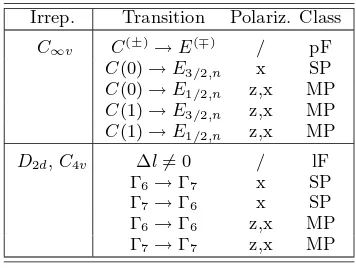
TABLE I: Summary of the polarizations allowed inC∞v,D2d and C4v symmetry for the different transitions considered. The directionsz andxrefer to orientations parallel and per-pendicular to the wire axis, respectively. The class to which each transition belongs is also indicated: pF and lF stand for parity-Forbidden and l-(angular momentum)-Forbidden; SP and MP stand for Single and Mixed Polarization, respec-tively.
Irrep. Transition Polariz. Class
C∞v C(±)→E(∓) / pF
C(0)→E3/2,n x SP
C(0)→E1/2,n z,x MP
C(1)→E3/2,n z,x MP
C(1)→E1/2,n z,x MP
D2d,C4v ∆l6= 0 / lF
Γ6→Γ7 x SP
Γ7→Γ6 x SP
Γ6→Γ6 z,x MP
Γ7→Γ7 z,x MP
III. GENERAL PROPERTIES OF WIRES WITH
C∞v ANDD2d SYMMETRIES
In aC∞v wire the irreducible representation of the
va-lence states at Γ are characterized19by the valueF
zof the
zcomponent of their total angular momentumF=J+L
(whereL is the angular momentum of the envelope part andJ the total angular momentum of the Bloch part of the wave function) and by their zone-center parity [even (+), or odd (-)] in the plane perpendicular to the wire, asEF(±z,n) , wheren refers to the order of the subband for the particular quantum numberFz. The conduction
perpendicular to the wire (henceforth when referring to “parity” we will always mean parity in the plane perpen-dicular to the wire), and the value of|Lz|, asC(±)(|Lz|).
In what follows we will consider interband transitions of the form C(±)(|L
z|) → EF(±z,n) (at zone center, tran-sitions between subbands with different parities, i.e., C(±)(|L
z|) → EF(∓z,n), are forbidden). The allowed tran-sitions can be divided into two general classes, depend-ing on their polarization: (i) mixed polarization (MP) transitions, that have both perpendicular (x) and paral-lel (z) component (to this class belong C(0) → E1/2,n,
C(1)→ E1/2,n and C(1) → E3/2,n19); (ii) single
polar-ization (SP) transitions, that are polarized only perpen-dicular to the wire axis, likeC(0)→E3/2,n19.
In a C4v square cross-section wire or aD2d
cylindri-cal wire instead, the conduction and valence subbands have Γ6 and Γ7 symmetry28. In order to determine the allowed and forbidden transitions in D2d wires we can
resort to considerations similar to those regarding the conservation of the parity quantum number, just made for C∞v wires. In this case the angular momentum l
of the envelope function needs to be conserved, there-fore transitions between subbands with different value of
l are formally forbidden. This criterion would yield the
same forbidden transitions inD2d wires as the parity
se-lection rule yielded inC∞v wires. However, we find that,
due to the strong confinement, the wire subbands do not have pure (s, p, d, etc.) character, but receive contri-butions from different angular momenta. This leads to a relaxation of the angular momentum conservation rule in D2d cylindrical wires. The interband Γi → Γj
tran-sitions (with i, j = 6,7), can again be grouped into two classes, as before: (i) the mixed polarization transitions include only Γi → Γi transitions, whereas to (ii) single
polarization transitions belong transitions between sub-bands with different symmetries. The explanation for the inclusion of a particular transition in one of the two classes derives from general group theoretical considera-tions. InC∞v,C4v andD2dwires, the component of the
dipole operator along thezaxis transforms as the identity representation19. Therefore, inC∞
vwires transitions
be-tween conduction subbands with Lz = 0 (C(0)) and
va-lence subbands withFz = 3/2 cannot occur if the optical
wave is polarized along the wire axisz. The same is true for transitions between subbands with different symme-tries in C4v and D2d wires. Transitions through optical
waves polarized perpendicular to the wire are however allowed. Table I summarizes the allowed polarizations for the different transitions considered and indicates the class to which each transition belongs.
1
e
2
e3 e
2
h
1
h h5
2
e3 e
1
e
1
h
5
h
5
h
4
h
d=1.2 nm d=3.6 nm d=9.6 nm
1
e
2
e3 e
1
h (p) (p)
(s) (d)
(s) (p) (p)
(p) (p) (d) (d) (s) (s)
−3
−4
−6 −5
(s) (s) (p) (f)
Energy (eV)
(s) (p) (p)
(s) (s)
[image:5.595.317.569.52.258.2](p) (p)
FIG. 1: Schematics of the calculated single-particle energy levels (labeled with their main angular momentum com-ponent) for 3 InAs D2d cylindrical wires with sizes d = 1.2,3.6,9.6 nm respectively. The dashed lines connect respec-tively CBM and VBM in the different wires. Only a few states are shown that were used in the calculations of the optical properties.
IV. ATOMISTIC DESCRIPTION OFD2d WIRES
The electronic structure of a nanostructure is calcu-lated by solving the single-particle Schr¨odinger equation:
·
−¯h 2
2m∇
2+V(r)
¸
ψi(r) =²iψi(r), (8)
whereV(r) is the potential and²ithe energy eigenvalues.
In the effective mass approximation, m is taken as the
effectivemass, and V =Vext(r) is anexternal potential
defining the geometric confinement of the nanostructure. We use a different approach, wherem=m0is the actual (bare) electron mass and the microscopic pseudopotential of the system Vps(r) is obtained as a superposition of
screened atomic potentials,
Vps(r) = Σi,αvα(r−Ri,α), (9)
where vα(r−Ri,α) is the atomic potential for an atom
of typeαlocated at the positionRi,α. The atomic
pseu-dopotentials are derived from the bulk LDA screened pseudopotential and fitted to reproduce the measured InAs bulk transition energies, deformation potentials and effective masses29. The total potential is then expressed as
V(r) =Vps(r) +Vnl (10)
where Vnl accounts for the nonlocal part of the
the system (nanostructure plus its surrounding matrix) in a supercell with periodic boundary conditions. The supercell size is chosen so as to minimize any interaction between neighbouring nanostructures This is obtained by increasing the supercell size until the calculated electron ground state energy does not change to within 1 meV (the hole energies converge much faster than the electron energies). We model LCG grown wires as free-standing, unstrained systems. In order to simulate the effect of an oxide coating, that is often present after the wire growth9, the nanostructures are embedded in a lattice-matched fictitious wide-gap (∼ 5.6 eV) material. This results in large band offsets and the absence of strain be-tween matrix and wire. The atoms occupy therefore the ideal positions of a perfect zinc-blende bulk crystal.
Due to the large number of atoms involved, we solve Eq. (8) by using the folded spectrum method30,31, whereby it is possible to calculate exactly only selected eigenstates of the Schr¨odinger equation around an arbi-trary reference energy ²ref. In this approach, Eq. (8) is replaced by:
·
− ¯h 2
2m0
∇2+Vps(r) +Vnl−²ref
¸2
ψi(r) = (²i−²ref)2ψi(r),
(11) which is equivalent to it in the sense that the ground
stateof Eq. (11) coincides with the solution of Eq. (8)
with energy closest to²ref. Therefore, with this method the band-edge states can be obtained by choosing the reference energy inside the band gap. The minimization procedure is carried out in a plane-wave basis set using a preconditioned conjugate-gradients algorithm. More details on this procedure can be found in Ref.31. With the single-particle energies and wave functions thus obtained, we calculate the inter-band transition energiesEcv=²c−
²v and dipole matrix elements:
M(i)
cv =hψv|pi|ψci (12)
where²v,ψv and²c,ψcare valence and conduction band
eigenenergies and wave functions, respectively, and pis the momentum operator with coordinatespi(i=x, y, z).
The emission spectrum is then calculated as a function of energy and temperature according to:
Icv(i)(E, T) =C P
c0,v0|M (i)
c0v0|
2e−(E−Ec0v0)2
λ2 e−
(E c0v0 −Ecv)
kB T
P c0,v0e
−(Ec0v0 −Ecv)
kB T
(13) whereC is a constant,λis the PL broadening, T is the temperature, and we take a Boltzmann average, where the sum overc0v0 is over states that satisfy E
c0v0 ≥Ecv,
to take into account temperature effects.
V. RESULTS
In order to investigate the role of microscopic structure and degree of valence-band coupling in the determination
of the wire optical properties, we calculated dipole matrix elements and degree of linear polarization for cylindrical wires with diameters in the range 1–10 nm, both in the finite (W/SO) and in the zero (N/SO) spin-orbit splitting approximation. In this way we were able to vary the mixing between Γ8-derived and Γ7-derived bands, which is maximum in the absence of SO interaction.
A. Single-particle energies of cylindrical InAs wires
Figure 1 shows schematically the electron and hole energy levels calculated with our atomistic method, to-gether with their main angular momentum component, relative to 3 InAs wire sizes: the thinnest,d= 1.2 nm, the thickest, d= 9.6 nm, and an intermediate size, d= 3.6 nm. We see that the energy gap and the energy splitting between the subbands decreases with increasing wire di-ameter, owing to the decreased size confinement effect. As we will see, this feature is one of the causes of the different temperature behaviour of the degree of linear polarization with different wire size.
B. Calculated polarizations and the role of dielectric mismatch
Figures 2 and 3 show the dipole matrix elements squared |M|2 and the relative degree of linear polar-ization, for the hi → ej (i = 1, . . . ,6 and j = 1,2,3)
transitions with light polarized along the wire axis (z-polarized) and perpendicular to it (x-(z-polarized). The x- and z-polarized matrix elements relative to the same transition are offset for clarity. The degree of linear po-larization shown was calculated from Eq. (6) considering only the anisotropy of the matrix elements but not the dielectric constant discontinuity between wire and sur-rounding material (i.e.,δ = 1). Indeed δ ≈1 in a wire covered by an oxide, where the two materials have sim-ilar dielectric constants. In the case of a free standing wire in vacuum (εout= 1), because of the small value of
δin Eq. (6), the anisotropy due to the dielectric constant discontinuity dominates over the contribution due to the matrix element anisotropy. Using our calculated matrix elements and the values of εin = 14.6 for the InAs
di-electric constant andεout = 1, we find that the degree of
0 0.04 0.08 0.12
|M|
2 (arb. units)
e1
,h
1
(a) Dipole elements
e1
,h
2
e1
,h
3
e1
,h
4
e1
,h
5
d = 3.6 nm
z-polarized x-polarized
e2
,h2
x10
e2
,h 3
e2
,h4
e2
,h 5
e3
,h1
x10
e3
,h2
e3
,h3
e3
,h4
e3
,h5
x10
1.15 1.2 1.25 1.3 1.35
0 0.2 0.4 0.6 0.8 1
Degree of Linear Polarization
|ρ|
(b) Polarization ratio
1.75 1.8 1.85 1.9
Transition energy (eV)
FIG. 2: (a) Matrix elements squared and (b) degree of linear polarization for the interband transitionshi→ej (i= 1, . . . ,5,
j= 1,2,3), as a function of the transition energy for thed= 3.6 nm InAs wire.
C. Symmetry considerations
Table II summarizes the irreducible representations of the first 3 conduction and 5 valence subbands inC∞v19,
D2dandC4v28wires with similar sizes. In aC∞vwire the
lowest conduction subbandC(+)(0) has even parity and is singly degenerate (excluding spin), whereas the next subbandC(−)(1) has odd parity and is doubly degener-ate (without spin). The uppermost subbandsh1, . . . , h5 in ad= 10 nm wire at zone center are19: E(+)
1/2,1,E (−) 1/2,2, E3(+)/2,1, E3(−/2),2, andE3(+)/2,3, respectively. In aL= 10 nm C4vsquare cross-section wire (whereLis the square side
dimension), instead, the lowest conduction states e1, e2 ande3have Γ626, Γ7and Γ7symmetry, respectively. The uppermost valence subbandsh1, . . . , h5in this case are28: Γ6, Γ7, Γ6, Γ7, and Γ7, respectively. In this work we find that, despite the identical labeling between the C4v
andD2d representations33, the ordering of both
conduc-tion and valence subbands in a L = 10 nm C4v square
cross-section and D2d cylindrical wires is different (see
Table II). In fact, although the isomorphism between the C4v and D2d groups specifies the possible
symme-tries of the subbands, it does not pose any constraint on their specific ordering, a feature which depends, among
other factors, on the magnitude of the confinement. It is therefore not inconsistent with our group theoretical con-siderations that the subbands in cylindrical and square cross-section wires have different order. This fact has important consequences on the allowed polarizations in several transitions. From Table II we see that the lowest conduction subbande1 and the uppermost valence sub-band h1 have the same symmetry (and the same main angular momentum component) in C4v and D2d wires.
[image:7.595.108.511.53.372.2]0 0.04 0.08 0.12
|M|
2 (arb. units)
e1
,h
1
e1
,h
2
e1
,h
3
e1
,h
4
e1
,h
5
x10
(a) Dipole elements d = 9.6 nm
x-polarized z-polarized
e2
,h2
e2
,h3 ,he2
4
x10 x10
x10
x10
e3 ,h1
e3
,h2
e3
,h3
e3
,h4
e3
,h5
0.83 0.84 0.85 0.86 0.87
0.620 0.63 0.64 0.65 0.66 0.67 0.2
0.4 0.6 0.8 1
Degree of Linear Polarization
|ρ|
(b) Polarization ratio
Transition energy (eV)
FIG. 3: (a) Matrix elements squared and (b) degree of linear polarization for the interband transitionshi→ej (i= 1, . . . ,5,
[image:8.595.108.513.52.361.2]j= 1,2,3), as a function of the transition energy for thed= 9.6 nm InAs wire.
TABLE II: Summary of the irreducible representations of the first 5 valence and 3 conduction subbands in wires withC∞v (d= 10 nm), D2d(d≥3.6 nm) andC4v (L= 10 nm) sym-metry.
Subband Representation
C∞(a)v D(2bd) C4(cv)
e1 C(+)(0) Γ6 Γ6 e2 C(−)(1) Γ7 Γ7 e3 C(−)(1) Γ6 Γ7
h1 E1(+)/2,1 Γ6 Γ6 h2 E1(−/2),2 Γ7 Γ7 h3 E3(+)/2,1 Γ7 Γ6 h4 E3(−/2),2 Γ6 Γ7 h5 E3(+)/2,3 Γ6 Γ7
aRef.19
bPresent calculation. cRef.26,28.
using the general arguments discussed in Section III we can deduce the polarizations allowed in all the transi-tions involving the first 3 conduction and 5 valence
sub-bands in wires withC∞v, C4v and D2d symmetry. The
results are summarized in Table III, which also contains our pseudopotential results. A consequence of the differ-ent subband ordering in C4v and D2d symmetry is that
transitions with particular polarizations that are forbid-den inC4v symmetry are allowed in D2d and vice versa.
Furthermore Table III also highlights two other impor-tant differences betweenD2d and C4v wires: (i) the
dif-ferent angular momentum composition of the subbands, which is manifested in different l-forbidden transitions; (ii) the fact that in continuous wires the subbands al-ways have purelcharacter, as opposed to atomistic wires where, as discussed in Section III, each subband receives contributions from different angular momentum compo-nents. The angular momentum selection rule is therefore relaxed inD2d wires and formally forbidden transitions
may become weakly allowed. We find that this mixing of l character in the wave functions of D2d wires increases
[image:8.595.115.239.478.612.2]to e3 is shown in the fact that, although both conduc-tion states have main pcharacter (and h1 main s), the e2 →h1 transition is forbidden (see Table III), whereas thee3→h1transition is very weakly allowed (see Figures 2a and 3a).
TABLE III: Summary of the polarization predicted for the transitionsei →hj (i= 1,2,3, h= 1, . . . ,5) for wires with (atomistic)D2d(d1 = 3.6 nm,d2 = 9.6 nm) and (continuum)
C∞v(d= 10 nm) andC4v(L= 10 nm) symmetry. The main angular momentum components obtained in the present cal-culation for each subband the are indicated in parenthesis. The directionsz andxrefer to orientations parallel and per-pendicular to the wire axis, respectively. In case of multiple polarizations, the first direction quoted is the one with the largest matrix element. We indicate in boldface the polar-izations that are found different between d1 and d2 for the same transition. Each transition is also labeled by the class to which it belongs, according to Table I.
Transition Polarization
EPM k·p
D2d(d1) D2d(d2) C∞(a)v C4(bv)
e1(s)→h1(s) z,x(MP) z,x(MP) z,x(MP) z,x(MP)
e1(s)→h2(p) x(SP) x(SP) pF x(SP)
e1(s)→h3(s,d)∗ x(SP) x(SP) x(SP) lF
e1(s)→h4(p) z,x(MP) x(MP) pF lF
e1(s)→h5(d,s)∗ z,x(MP) z,x(MP) x(SP) x(SP)
e2(p)→h1(s) lF lF pF lF
e2(p)→h2(p) z,x(MP) z,x(MP) z,x(MP) lF
e2(p)→h3(s,d)∗ x,z(MP) z,x(MP) pF x(SP) e2(p)→h4(p) x(SP) x(SP) z,x(MP) z,x(MP)
e2(p)→h5(d,s)∗ x(SP) lF pF lF
e3(p)→h1(s) x(MP) z(MP) pF lF
e3(p)→h2(p) x(SP) x(SP) z,x(MP) lF
e3(p)→h3(s,d)∗ x(SP) x(SP) pF x(SP) e3(p)→h4(p) z,x(MP) z,x(MP) z,x(MP) z,x(MP)
e3(p)→h5(d,s)∗ x,z(MP) z,x(MP) pF lF ∗The angular momentum componentssanddhave similar
magnitudes.
aRef.19
bThe polarization ofe1→h
jtransitions is from Ref.26, that of transitions involvinge2 ande3 has been deduced from group theory arguments.
D. Near band-gap transitionshi→e1
The fundamental band-gap h1 → e1 transition has both z and x polarizations, but is mainly polarized along the wire axis in all wire symmetries considered in Ta-ble III. We find that, in the absence of SO interaction (∆so= 0 eV), in a circular cross-section wire with
atom-istic D2d symmetry it is 100% z-polarized (i.e., the h1 state does not interact at all with optical waves polar-ized normal to the wire axis). When the coupling be-tween bulk Γ8v- and Γ7v-derived valence bands is restored
0.5 0.6 0.7 0.8 0.9 1
Degree of Linear Polarization
|
ρ
|
N/SO
W/SO
T = 2K
T = 300K all T
(a) Polarization ratio
2 4 6 8 10
Wire diameter d (nm)
[image:9.595.59.295.274.486.2]0 0.1 0.2
|M(e1,h1)|
2
(arb. units)
N/SO
W/SO
W/SO
N/SO
z-polarized
x-polarized (b) Dipole matrix
elements
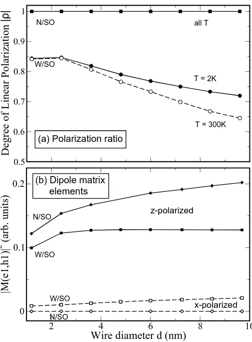
FIG. 4: (a) Degree of linear polarization of the fundamental transitionh1→e1 as a function of wire diameter, calculated atT= 2 K andT= 300 K both considering (W/SO) and not considering (N/SO) SO splitting. (b) Dipole matrix elements, for the same transition, polarized parallel (z) and perpendic-ular (x) to the wire axis, in the finite and zero SO splitting approximations.
to its actual value (with ∆so = 0.4 eV in bulk InAs)
the degree of linear polarization decreases by about 20% and becomes size and temperature dependent. Figures 4 and 5 show the temperature dependence of our calculated dipole matrix elements and degree of linear polarization in the finite and zero SO approximations. This decrease ofρ from 100% to about 80% with increasing SO split-ting, together with the value of 60% obtained forρin the infinite spin-orbit approximation17,19,21, show that linear polarization effects in actual 1D systems are due to sub-stantial mixing between the four bulk Γ8v- andthe two
Γ7v-derived valence bands.
The next transition (h2 → e1), is a Γ7 → Γ6 transi-tions in bothD2d andC4v wires and is therefore allowed
to be polarized only perpendicular to the wire axis. The h2 → e1 and the h4 → e1 transitions are forbidden in C∞v19 QWRs, due to the different parity of the
0 50 100 150 200 250 300
T (K)
0.6 0.65 0.7 0.75 0.8 0.85
Degree of Linear Polarization
ρ
1.2 2.4
3.6
4.8
6.0
7.2
8.4
9.6
[image:10.595.54.305.48.226.2]h
1e
1FIG. 5: Degree of linear polarization of the fundamental tran-sitionh1→e1as a function of temperatureTfor the different wire diameters considered.
zerol= 1 component of e1 we find that they are weakly allowed: the dipole matrix elements for these transitions decrease by over one order of magnitude with increasing wire diameter (i.e., with decreasingl mixing ine1), from 2.4 nm to 9.6 nm (both becoming less than 1% of the value of the matrix element relative to the band gap tran-sition in thed= 9.6 nm wire). As theh3→e1transition is only x-polarized in C∞v wires, the two lowest energy
transitions have opposite polarizations inD2d,C4v, and
C∞v wires. The fundamental transition is in fact
polar-ized mainly along the wire axis while the next allowed transition has onlyxpolarization in all symmetries. The h4 → e1 transition, instead, being a transition between two Γ6subbands, can have both polarizations: however, ind >4.8 nmD2dstructures, it is only polarized
perpen-dicular to the wire. The polarization component parallel to the wire axis increases from zero34 to a value which is larger than that of the perpendicular component, when the wire diameter decreases from 9.6 nm to 3.6 nm.
1. Temperature dependence
We find (Fig. 4 and Fig. 5) a stronger temperature dependence forρ(h1 →e1) in thick wires: in a d= 9.6 nm wire ρdecreases by 10% with a 300 K temperature increase, compared to a 0.25% decrease in ad= 1.2 nm wire, for the same temperature variation. This size de-pendence of the polarization can be understood in terms of lateral confinement effects. Due to the quantum size effect, thin wires experience a stronger confinement than thicker wires, which means that they have a higher netic energy introduced by the confinement. As this ki-netic energy is responsible for the mixing20of the valence bands at zone center, thin wires have also a stronger mix-ing and therefore a higher degree of linear polarization. Furthermore, due to the larger confinement, the hole
en-ergy levels are farther apart in thin wires than they are in thicker wires (see Fig. 1), and their density of states is lower close to the band edge. Therefore in thin wires at low temperature theh1→e1transition is the most prob-able and the degree of polarization is high (see Fig. 6). In the case of thick wires the probability forh2,3→e1 tran-sitions, which as we mentioned before, unlike theh1→e1 transition are polarized only perpendicular to the wire, increases with T. This reduces the degree of linear polar-ization with increasing temperature in thick wires. This is clearly seen in Fig. 6, where we show the PL polar-ization spectra (with 50 meV broadening) around the en-ergy of the fundamentalh1→e1transition, calculated at T = 2 K andT = 300 K for ad= 1.2 nm and ad= 9.6 nm wire. The different density of states also explains the larger blue shift (7 meV) of the x-polarized PL that takes place in thick wires with a temperature increase of 300 K, compared to that (2 meV) occurring in thin wires (Figure 6). The detectability of PL polarization peaks in these wires is, however, closely related to the experimen-tal line broadening. As shown in Fig. 7, if the broadening is larger than 20 meV at room temperature (in typical experimental conditions it is > 50 meV1), the peak in the x-polarized emission corresponding to the h3 → e1 transition, found in Fig. 3, is masked by the broadening of the fundamental transition in ad= 9.6 nm wire. In ad= 1.2 nm wire (Fig. 7), even if the broadening is of the order of 40 meV, the second peak in the x-polarized emission can still be seen as a shoulder on the high en-ergy side of the main peak, but is almost completely lost in it for broadenings≥50 meV. Therefore this peak has not been seen in cylindrical LCG wires of any size, due to the present experimental accuracy.
E. Higher energy transitionshi→e2,3
Theh1→e2 transition is found to be forbidden in all wires considered in Table III. Theh2→e2 andh3→e2 transitions in Fig. 2 (Γ7→Γ7 transitions inD2d wires)
are both x- and z-polarized. The former transition has a stronger parallel component that increases with wire di-ameter, while the perpendicular component stays almost constant. In theh3→e2transition (weakly allowed only because of the non zerol= 2 component of thee2 sub-band inD2dwires, and parity-forbidden inC∞v19wires),
instead, the perpendicular component decreases by more than one order of magnitude with increasingd, becoming smaller than the parallel component ford >3.6 nm (see Table III). The h4 → e2 and h5 → e2 transitions are Γ6 → Γ7 transitions in D2d QWRs and can, therefore,
only be x-polarized. The former, however, is predicted to have both polarizations in C∞v19 QWRs, where the
k component is the strongest. The h5 → e2 transition that we only find very weakly allowed in small (d ≤ 6 nm)D2dwires, due to the higherlmixing in these
2.6 2.7 2.8 2.9 0
0.02 0.04 0.06 0.08
0.1 T = 2K
T = 300K (a) d = 1.2 nm
z
x
e1
,h1
e1
,h2
0.5 0.6 0.7 0.8
Energy (eV)
0 0.04 0.08 0.12
(b) d = 9.6 nm z
z
x x
e 1
,h1
e1
,h 5
[image:11.595.55.570.47.388.2]PL intensity (arb. units)
FIG. 6: PL polarization spectra around the energy of the fundamentalh1 →e1 transition, calculated atT = 2 K and T = 300 K for a (a)d= 1.2 nm and a (b)d= 9.6 nm wire (with 50 meV broadening). The arrows mark the position in energy of the transitionshi→e1, withi= 1, . . . ,5.
D2d wires) h1 →e3 and h5 →e3 transitions, forbidden in low symmetry wires19 have opposite polarizations in the two wires of Fig. 2: h1→e3 is z-polarized ind >6 nm wires and x-polarized ind≤6 nm wires; in h5→e3 both polarizations are present, but the⊥component de-creases with increasing d, becoming smaller than the k component ford >6 nm.
As a rule we find that whenever a transition is for-mally angular-momentum-forbidden inD2d QWRs (and
parity-forbidden in lower symmetry wires), the ⊥ com-ponent decreases (very often by more than one order of magnitude) with increasingdinD2dQWRs, resulting
ei-ther very weak or non existent altogeei-ther in thick wires.
F. In-plane optical anisotropies
In an attempt to include microscopic features in the k·p treatment in the infinite spin-orbit split-ting approximation, Yamaguchi and Usui21 derived
2.6 2.7 2.8 2.9 0
0.002 0.004 0.006
0.008 10 meV20 meV 30 meV 40 meV 50 meV T = 300 K
d = 1.2 nm x-polarized
z-polarized
e,h1
1
e,h1
2
(50 meV)
(a)
0.5 0.55 0.6 0.65 0.7 0.75
Energy (eV)
0 0.01 0.02 0.03 0.04 0.05
10 meV 20 meV 30 meV d = 9.6 nm
T = 300 K
e1
,h1
e1
,h 3
e1
,h5
(b)
PL intensity (arb. units)
FIG. 7: PL polarization spectra atT = 300 K calculated for ad = 1.2 nm (a), and a d = 9.6 nm (b) wire for different values of the line broadening.
a crystallographic-orientation-dependent expression for the dipole matrix element, which led to an in-plane anisotropy. In the spherical approximation for the va-lence bands (in which the Luttinger parameterγ2 =γ3) there is no polarization anisotropy in the plane normal to the wire axis in a C∞v wire21. By including the
ef-fect of valence-band anisotropy, Yamaguchi and Usui21 predicted a weak dependence on the wire orientation for the polarization alongz, and a strong dependence for the polarization along two perpendicular directionsxand y (both in-plane) for the fundamental transition in wires oriented in directions different than [001] and [111]. Fur-thermore, only for [001]- and [111]-oriented wires they found no in-plane anisotropy, i.e.,|Mx| =|My|. For all
other orientations the calculated dipole matrix elements alongxandy were different.
Similarly, we find no in-plane anisotropy in the fun-damental transition in D2d wires. However, higher
en-ergy transitions show polarization anisotropy in the plane perpendicular to the wire axis. Figures 8 and 9 show thexy-plane (⊥to the wire axis) anisotropy we find in the h4 → e1 and h5 → e1 transitions in D2d QWRs,
0.05 0.1 0.15 0.2 0.25
E(h 4,e1)
-Eg (eV)
0 0.05 0.1 0.15
Degree of Linear Polarization
|
ρ
’|
(b)
0 2×10⁻⁴ 4×10⁻⁴ 6×10⁻⁴
|M|
2 (arb. units)
(1-10)-polarized (110)-polarized
9.6 7.26.0 4.8 3.6 2.4
d (nm)
x10-1
x10-2 h
4 e1
(a)
FIG. 8: (a) In-plane matrix elements squared and (b) degree of linear polarization for the interband transitionsh4 →e1, as a function of the transition energy measured from the band gap (lowerxaxis) and wire diameter (upper xaxis), in D2d InAs wires.
from that along the [1¯10] direction. We see that the h4 → e1 transition is prevalently [110]-polarized with only the d = 9.6 nm wire polarized along [1¯10]. The opposite is true for the h5 → e1 transition, where the only size for which the transition is prevalently polarized along [110] is d= 6 nm. However the d= 9.6 nm wire is found mainly polarized along [1¯10] and the d= 6 nm wire mainly along [110], in both transitions. In all other transitions considered we found no anisotropy in thexy plane.
VI. SUMMARY
In summary we applied an atomistic, empirical pseu-dopotential method to calculate optical transitions in free-standing, unstrained [001]-oriented cylindrical InAs quantum wires with diameters in the experimentally ac-cessible range 10-100 ˚A. We found evidence of strong
cou-pling of bulk Γ8v- and bulk Γ7v-derived bands in the size
and temperature dependence of the linear anisotropies of
0.05 0.1 0.15 0.2 0.25
E
(h5,e1)-Eg (eV) 0
0.1 0.2 0.3 0.4
Degree of Linear Polarization
|
ρ
’|
(b)
0 0.001 0.002
|M|
2 (arb. units)
(1-10)-polarized (110)-polarized
9.6 7.2 6.0 4.8 3.6 2.4
d (nm)
h5 e1 (a)
FIG. 9: (a) In-plane matrix elements squared and (b) degree of linear polarization for the interband transitionsh5 →e1, as a function of the transition energy measured from the band gap (lowerxaxis) and wire diameter (upperxaxis), in D2d InAs wires.
optical transitions in QWRs. We show that simple ap-proaches, that model the wire as a continuum with no underlying crystal structure, miss some optical transi-tions, due to their strict application of conservation rules that we found to be relaxed in strongly confined atomistic nanostructures.
VII. ACKNOWLEDGMENTS
The authors thank G. Bester for many valuable com-ments and suggestions and for his accurate reading of the manuscript.
[image:12.595.57.303.50.397.2] [image:12.595.322.566.76.418.2]1 J. Wang, M. S. Gudiksen, X. Duan, Yi Cui, C. M. Lieber,
Science 293, 1455 (2001).
2 Yu Huang, X. Duan, Q. Wei, C. M. Lieber, Science 291,
630 (2001).
3 M. S. Gudiksen, J. Wang, and C. M. Lieber, J. Phys.
Chem.105, 4062 (2001).
4 Y. Wu and P. Yang, J. Am. Chem. Soc.123, 3165 (2001). 5 Yi Cui, L. J. Lauhon, M. S. Gudiksen, J. Wang and C.
M. Lieber, Appl. Phys. Lett.78, 2214 (2001); X. Duan, J. Wang, and C. M. Lieber, Appl. Phys. Lett. 76, 1116 (2000).
6 X. Duan and C. M. Lieber, J. Am. Chem. Soc. 122, 188
(2000); M. S. Gudiksen and C. M. Lieber, J. Am. Chem. Soc.122, 8801 (2000).
7 X. Duan and C. M. Lieber, Adv. Mater.12, 298 (2000). 8 J. Hu, T. W. Odom, and C. M. Lieber, Acc. Chem. Res.
32, 435 (1999).
9 A. M. Morales and C. M . Lieber, Science279, 208 (1998). 10 E. Kapon, D. M. Hwang, R. Bhat, Phys. Rev. Lett. 63,
430 (1989).
11 M. Tsuchiya, J. M. Gaines, R. H. Yan, R. J. Simes, P. O.
Holtz, L. A. Coldren, P. M. Petroff, Phys. Rev. Lett.62, 466 (1989).
12 M. Kohl, D. Heitmann, P. Grambow, K. Ploog, Phys. Rev.
Lett.63, 2124 (1989).
13 H. Akiyama, T. Someya, H. Sakaki, Phys. Rev. B 53,
R4229 (1996).
14 T. Sogawa, H. Ando, S. Ando, H. Kanbe, Phys. Rev. B56,
1958 (1997).
15 F. Vouilloz, D. Y. Oberli, M.-A. Dupertuis, A. Gustafsson,
F. Reinhardt, E. Kapon, Phys. Rev. Lett.78, 1580 (1997).
16 J. A. Brum and G. Bastard, Superlatt. Microstruct.4, 443
(1988).
17 P. C. Sercel and K. J. Vahala, Appl. Phys. Lett.57, 545
(1990).
18 P. C. Sercel and K. J. Vahala, Phys. Rev. B 42, 3690
(1990).
19 P. C. Sercel and K. J. Vahala, Phys. Rev. B 44, 5681
(1991).
20 U. Bockelmann and G. Bastard, Phys. Rev. B 45, 1688
(1992).
21 A. A. Yamaguchi and A. Usui, J. Appl. Phys. 78, 1361
(1995).
22 P. Ils, Ch. Greus, A. Forchel, V. D. Kulakovskii, N. A.
Gippius, S. G. Tikhodeev, Phys. Rev. B51, 4272 (1995).
23 E. A. Muljarov, E. A. Zhukov, V. S. Dneprovskii, Y.
Ma-sumoto, Phys. Rev. B62, 7420 (2000).
24 M. A. Dupertuis, E. Martinet, D. Y. Oberli, E. Kapon,
Europhys. Lett.52, 420 (2000).
25 W. H. Zheng, J.-B. Xia, K. W. Cheah, J. Phys. Condens.
Matter9, 5105 (1997).
26 D. S. Citrin, Y.-C. Chang, J. Appl. Phys.70, 867 (1991). 27 G. Bester, S. Nair. A. Zunger, Phys. Rev. B 67, 161306
(2003).
28 D. S. Citrin and Y.-C. Chang, Phys. Rev. B 40, 5507
(1989).
29 L. W. Wang and A. Zunger, Phys. Rev. B 51, 17 398
(1995); H. Fu and A. Zunger, Phys. Rev. B56, 1496 (1997).
30 L. W. Wang and A. Zunger, J. Chem. Phys. 100, 2394
(1994); J. Phys. Chem.98, 2158 (1994).
31 L. W. Wang and A. Zunger, in Semiconductor
Nanoclus-ters, edited by P. V. Kamat and D. Meisel (Elsevier, New York, 1996).
32 L. D. Landau and E. M. Lifshitz,Electrodynamics of
con-tinuous media, (Moscow, Nauka 1992).
33 G. F. Koster, J. O. Dimmock, R. G. Wheeler, H. Slatz,
Properties of the Thirty-Two Point Groups (MIT Press,
Cambridge, Mass., 1966).
34 We assume a matrix element|M(i)|2 (i=k,⊥) to be zero
when its value is<∼10−4|Mek1,h1|2.
35 W. T. Masselink, Y.-C. Chang, H. Morkoc, Phys. Rev. B