Int. J. Electrochem. Sci., 11 (2016) 5819 – 5828, doi: 10.20964/2016.07.72
International Journal of
ELECTROCHEMICAL
SCIENCE
www.electrochemsci.orgImproving Power Conversion Efficiency of P3HT/PCBM based
Organic Solar Cells by Optimizing Graphene Doping
Concentration and Annealing Temperature
Shang-Chou Chang1,*, Yu-Jen Hsiao2, ,Tien-Chai Lin1, To-Sing Li 1, Syu-An Zeng1, ,Chen-En Yu 1
1
Department of Electrical Engineering, Kun Shan University, Tainan City 71010, Taiwan
2
National Nano Device Laboratories, Tainan City 74147, Taiwan
*
E-mail: [email protected]
Received: 19 April 2016 / Accepted: 23 May 2016 / Published: 4 June 2016
Graphene (GN) doping concentration and annealing temperature in blended poly (3-hexylthiophene) and [6,6]-phenyl C61 butyric acid methyl ester (P3HT/PCBM) with GN (P3HT/PCBM /GN) based organic solar cells (OSC) were investigated. Results indicate the power conversion efficiency (PCE) of P3HT/PCBM /GN based OSC can be efficiently increased by 3 wt% GN doping and 120oC annealing. The OSC doped with 3 wt% GN exhibited the highest PCE among OSC doped with 0~10 wt% GN under the same annealed condition: unannlealed status and 120oC annealing. The PCE of 120oC annealed OSC doped with 3 wt% GN is 2.81, which is almost two times higher than that doped with 10 wt% GN. Thermal desorption spectra of unannealed P3HT/PCBM /3 wt% GN show two desorption peaks at around 130 and 182oC resulting from water vapor. The two temperatures are close to the glass transition temperature of PCBM and melting temperature of P3HT, respectively. The 120oC annealing on P3HT/PCBM/3 wt% GN can make both P3HT and PCBM have relatively good crystallization compared with unannealed status and 170oC annealing. Good crystallization makes charge carriers transport easily in P3HT/PCBM/3 wt %GN based OSC.
Keywords: power conversion efficiency, P3HT/PCBM, grapheme
1. INTRODUCTION
(P3HT) and [6,6]-phenyl C61 butyric acid methyl ester (PCBM) blend have been intensively investigated[5,6]. The OSC composed of π-conjugated polymers and fullerene derivatives have attracted considerable interest due to their lightness, simple solution processing and bending capability.[7,8] The power conversion efficiency (PCE) of OSC can be improved by doping nanomaterials like carbon nanotubes [9,10], nanodiamonds [11], Fe3O4 magnetic nanoparticles [12], and ZnO nanorods [13]. Nanomaterials, which can be used to make super strong metals [14], have applied in solar cells due to their high surface to volume ratio, quantum confinement and quantum size effect [15]. Our group has doped Si nanoparticles, CdSe core-shell nanoparticles and nano-diamonds respectively into OSC, and the results indicate the PCE of OSC can be all improved with an upper limit of doping concentration.[16-18].
With superior electron transport properties, graphene (GN) has been well adjusted in OSC as both the electron acceptor material and the transparent electrode [19, 20]. However, their efficiency is extremely confined as compared with fullerene derivatives by reason of their conductor characteristics, which interrupt the effective hole mobility and aid the formation of recombination pathways [21].
Doping nanomaterials into photoactive layer can make positive effects such as increasing interfaces between donors and acceptors, optical absorption on photovoltaic performance. However, negative effects may also arise when nanomaterials are doped into OSC. Doping nanoparticles into P3HT/PCBM based OSC decreases the performance of OSC due to quenching of the excited state in the polymer. Segregation phenomena in OSC due to over doping have been reported [22]. Our experiences in doping nanomaterials into P3HT/PCBM reveal that the existence of the optimum doping concentration corresponds to PV characteristics of processed OSC[16-18].
Thermal annealing can provide benefits on photovoltaic process of P3HT/PCBM based OSC, such as improvement in surface morphology and crystallinity of photoactive materials, furthermore contact resistance between active materials and electrode to aid charge generation, transport and collection [23]. However, thermal annealing can also bring problems on photovoltaic process of P3HT/PCBM based OSC if thermal annealing is too much, like PCBM aggregation, phase separation between P3HT and PCBM to lower PCE [24]. Selecting annealing temperature is one of the key factors in improving short circuit current density (Jsc), open circuit voltage (Voc) and PCE [25].
Selecting optimum annealing temperature of nanodiamonds doped P3HT/PCBM has been studied with thermal desorption spectroscopy in our group [18]. The results indicate 120oC is the optimum annealing temperature for nanodiamonds doped P3HT/PCBM based OSC.
This paper investigates influence of GN doping concentration and annealing temperature in processing P3HT/PCBM/GN based OSC on photovoltaic properties. Photovoltaic characteristics of the P3HT/PCBM based OSC with different GN doping concentration were measured first. The obtained OSC with the optimum GN concentration were annealed with different annealing temperature. The optimized GN doping concentration and annealing temperature to produce P3HT/PCBM/GN based OSC were obtained in this work.
2. EXPERIMENTS
tool to raise hydrophilic property of the ITO surface. A layer of poly(3,4-ethylenedioxythiophene)/poly(styrenesulfonate) (PEDOT/PSS, CLEVIOS™ P VP AI 4083, Heraeus Clevios GmbH, Leverkusen, Germany) about 40 nm thick was spin-coated on the ITO substrate and baked at 120 oC for 30 min. The photoactive layer composed P3HT (RMI-001E, Rieke Met. Inc., Lincoln, Nebraska, USA) and PCBM ([60]PCBM, Nano-C, Westwood, Maryland, USA) in 10:8 wt % ratio dissolved in 1,2-dichlorobenzene with 0, 1, 3, 5, 10 wt% GN. Some samples were annealed at 120oC according to our previous optimizing results on other PCBM/P3HT based OSC [16-18]. Lastly, a Ca/Al electrode about 120 nm thick was thermally evaporated on the active layer.
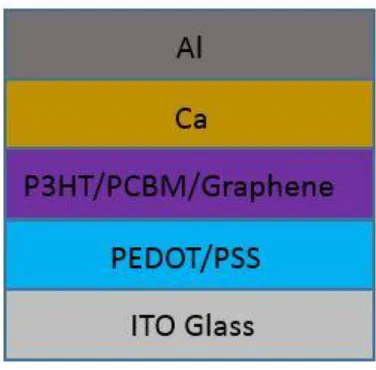
[image:3.596.202.390.269.454.2]The device structure of the produced OSC, in which P3HT/PCBM/GN is the photoactive layer of the device, was shown in figure 1.
Figure 1. Device structure of P3HT/PCBM/Graphene based photovoltaic device
photovoltaic properties of P3HT/PCBM/3 wt% GN annealed at 120 and 170oC based OSC were estimated.
3. RESULTS AND DISCUSSION
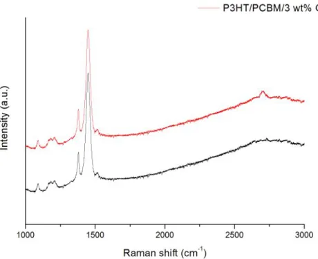
The measured Raman spectra of OSC with GN doping show an apparent peak corresponding to GN. Figure 2 shows two spectra corresponding to OSC undoped and doped with 3 wt% GN respectively. The peak at about 2700 cm-1 corresponds to G’ band of graphene resulted from OSC doped with 3 wt% GN in figure 2 [26]. The peak at about 1442 and 1380 cm-1 can be attributed to C=C stretching vibrations of the thiophene ring and C-C skeletal stretching in P3HT respectively [27].
Figure 2. The measured Raman spectra corresponding to OSC undoped and doped with 3 wt% GN
[image:4.596.185.415.287.474.2]
B
C
[image:5.596.179.439.72.626.2]D
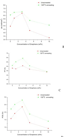
Figure 3. Photovoltaic performance: a. open circuit voltage (Voc), b. short circuit current density (Jsc), c. fill factor (FF) and d. power conversion efficiency(PCE) of unannealed and 120oC annealed P3HT/PCBM/GN with different GN doping concentrations
and 3d respectively. The OSC with 3 wt% GN demonstrates the highest value of all four parameters in figure 3 for both unannealed and 120oC annealed OSC. The PCE of 120oC annealed OSC rises from 2.24 to 2.81% with GN doping concentration till 3 wt%. The GN doping raises the donor/acceptor interface area for charge separation and reduces the electron transfer path in P3HT/PCBM. However, over 3 wt% GN doping provides problems like segregation phenomena in polymer [22]. The PCE of 120oC annealed OSC with 10 wt% GN doping is almost two times lower than that with 3 wt% GN doping observed from figure 3d. The Jsc, FF and PCE of 120oC annealed OSC is higher than those of unannealed OSC for the same GN doping concentration observed from figure 3b , 3c and 3d. Annealing can improve nanoscale morphology and crystallinity of photoactive layer. Photovoltaic performance is therefore improved by thermal annealing.
Figure 4. Thermal desorption spectroscopy of unannealed P3HT/PCBM/3 wt %GN films
The TDS of unannealed P3HT/PCBM/3 wt% GN films was displayed in figure 4. Only one desorption species clearly observed from TDS measurement system corresponds to ion mass to charge ratio: 18. The species attributes water vapor. This may relate with significantly hygroscopic PEDOT:PSS and PCBM contained in measured OSC [28-29]. Two desorption peaks at around 130 and 180oC in figure 4 similar to those we investigated on OSC whose photoactive materials are P3HT/PCBM/ doped with nano diamonds [18]. The two temperatures attribute to the reported glass transition temperature of PCBM (131.2oC) and melting temperature of P3HT (178oC) [30, 31]. These two desorption peaks in figure 4 correspond to two activated states connected with glass transition temperature of PCBM and melting temperature of P3HT in P3HT/PCBM/3 wt % GN.
[image:6.596.146.417.277.476.2]
Figure 5. Optical absorption spectra of P3HT/PCBM/3 wt% GN annealed at different annealing temperatures (unannealed, 120, 170oC).
[image:7.596.140.440.85.317.2]The intensity of optical absorption in figure 5 relates with crystallization of photoactive materials. PCBM crystallizes faster than P3HT, and can homogeneously grow crystals at room temperature [32]. Annealing enhances the crystallization of P3HT and disconnection of PCBM in P3HT/PCBM. PCBM disconnects and constructs isolated clusters as its crystals start to break-up during annealing process [33].
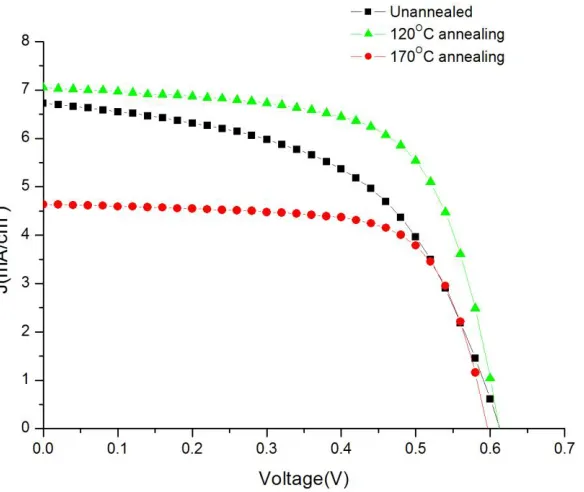
Table 1. Photovoltaic characteristics of the P3HT/PCBM/3 wt% GN based OSC annealed at different temperatures (unannealed, 120, 170oC).
Photovoltaic Characteristics
Annealing status Voc (V) Jsc (mA/cm
-2
) FF (%) PCE (%)
Unannealed 0.619 6.84 55.83 2.36
120∘C annealing 0.619 7.05 64.30 2.81
170∘C annealing 0.599 4.63 68.16 1.89
[image:7.596.41.552.545.660.2]
Figure 6. Current density-voltage (J–V) characteristics of the P3HT/PCBM/3 wt% GN based OSC annealed at different temperatures (unannealed, 120, 170oC).
The magnitude sequence of PCE for OSC in table 1 is: 120oC > unannealed > 170oC. The first desorption peak at 130oC in figure 3 corresponds to a turning point in P3HT/PCBM based OSC. The 130oC peak corresponds to glass transition temperature of PCBM. Crystallization of P3HT and PCBM is critical for photovoltaic characteristics of the P3HT/PCBM based OSC. Well crystallized P3HT/PCBM enhances charge carriers move easily in photoactive layer during photovoltaic process. Annealing at 120oC is close but lower than the turning point : 130oC can cause P3HT as well as PCBM in P3HT/PCBM/3 wt %GN have comparatively good crystallization seen from the trend of absorption intensity in figure 5.
4. CONCLUSIONS
[image:8.596.154.446.81.327.2]
which in turn aids transport of charge carriers in P3HT/PCBM/3 wt% GN based OSC. The P3HT/PCBM based OSC with 3 wt% GN doping and 120oC annealing on photoactive layer exhibit optimized doping concentration and annealing temperature.
ACKNOWLEDGEMENTS
The authors would like to thank the Ministry of Science and Technology Taiwan for financially supporting this research under grant MOST 104-2221-E-168 -015 -, and National Nano Device Laboratories for equipment support.
References
1. S. Günes, H. Neugebauer, and N. S. Sariciftci, Chemical Reviews, 107(4)(2007)1324. 2. P.V. Kamat, Journal of Physical Chemistry C, 111(2007)2834.
3. P.V. Kamat, The Journal of Physical Chemistry C, 112(2008)18737.
4. B.R. Saunders and M.L. Turner, Advances in Colloid and Interface Science, 138(2008)1.
5. S.W. Lee, H.J. Lee, J.H. Choi, W.G. Koh, J.M. Myoung, J.H. Hur, J.J. Park, J.H. Cho, U. Jeong, Nano Letters, 10(2010)347.
6. G. Li, V. Shrotriya, J.S. Huang, Y. Yao, T. Moriarty, K. Emery, Y. Yang, Nature Materials, 4(2005) 864.
7. T. F. Guo, T. C. Wen, G. L. Pakhomov, X. G. Chin, S. H. Liou, P. H. Yeh, Thin Solid Films, 516(2008)3138.
8. F. C. Chen, J. L. Wu, C. L. Lee, W. C. Huang, H. M. Chen, W. C. Chen, IEEE Electron Device Lett., 30(2009)727.
9. M.C. Wu, Y.Y. Lin, S. Chen, H.C. Liao, Y.J. Wu, C.W. Chen, Y.F. Chen, and W.F. Su, Chemical Physics Letters, 468(1–3)(2009)64.
10.Y. Hsiao, T. Fang, L. Ji, Y. Lee, and B. Dai, Electrochemistry Communications, 18(1)(2012)4. 11.W. Zhang, Y. Xu,H.Wang, C. Xu, and S. Yang, Solar Energy Materials and Solar Cells,
95(10)(2011)2880.
12.S. V. Bhat, A. Govindaraj, and C. N. R. Rao, Solar Energy Materials and Solar Cells, 95(8)(2011) 2318.
13.R. Valiev, Nature, 419(6910)(2002)887.
14.S. Q. Feng, D. P. Yu, H. Z. Zhang, Z. G. Bai, and Y. Ding, Journal of Crystal Growth, 209(2-3)(2000)513.
15.A. C. Varonides, Renewable Energy, 33(2)(2008)273.
16.S.-C. Chang, Y.-J. Hsiao, T.-S. Li, Journal of Nanomaterials, 2013 (2013), Article ID 354035. 17.S.-C. Chang, Y.-J. Hsiao, T.-S. Li, Journal of Electronic Materials, 43 (2014) 3077.
18.S.-C. Chang, Y.-J. Hsiao, T.-S. Li, International Journal of Electrochemical Science, 10 (2015) 1658.
19.Z.F. Liu, Q. Liu, Y. Huang, Y.F. Ma, S.G. Yin, X.Y. Zhang, W. Sun, Y.S. Chen, Adv.Mater. 20 (2008) 3924.
20.J.B. Wu, H.A. Becerril, Z.N. Bao, Z.F. Liu, Y.S. Chen, P. Peumans, Appl. Phys. Lett.92 (2008) 263302.
21.E. Kymakis, P. Servati, P. Tzanetakis, E. Koudoumas, N. Kornilios, I. Rompogiannakis,Y. Franghiadakis, G.A.J. Amaratunga, Nanotechnology 18 (2007) 435702.
22.K. Topp, H. Borchert, F. Johnen, A. V. Tunc, M. Knipper, E. V. Hauff, J. Parisi and K. Al-Shamery, J. Phys. Chem. A, 114(2010) 3981.
24.M. J. Greaney, S. Das, D. H. Webber, S. E. Bradforth, and R. L. Brutchey, ACSNANO, 6(2012)4222.
25. . Albero, P. Riente, . N. Clifford, M. A. Peric s, and E. Palomares, The Journal of Physical Chemistry C, 117(2013)13374.
26.L.M. Malard, M.A. Pimenta, G. Dresselhaus, M.S. Dresselhaus, , Physics Reports 473 (2009) 51. 27.M. Baibarac, M. Lapkowski, A. Pron, S. Lefrant and I. Baltog, Journal of Raman Spectroscopy,
29(1998)825.
28.A. Guerrero, P. Boix, L. F. Marchesi, T. Sanchis, F. C.Pereira and G. Garcia-Belmonte, Solar Energy Materials & Solar Cells, 100(2012)185.
29.P. E. Hopkinson, P. A. Staniec, A. J. Pearson , A. D. F. Dunbar , T. Wang , A. J. Ryan , R. A. L. Jones, D. G. Lidzey , and A. M. Donald, Macromolecules, 44(8)(2011)2908.
30.D. Chirvase, J. Parisi, J. C. Hummelen and V. Dyakonov, Nanotechnology, 15(9)(2004)1317. 31.W.H. Lee, S.Y. Chuang, H.L. Chen , W.F. Su and C.H. Lin, Thin Solid Films, 518(2010)7450. 32.G. Kalonga, G. K. Chinyama, M. O. Munyati and M. Maaza, Journal of Chemical Engineering and
Materials, 4(7)(2013)93.
33.D Chirvase, J Parisi, J C Hummelen and V Dyakonov, Nanotechnology, 15(9)(2004)1317.