Development and Optimization of Durable
Microelectrodes for Quantitative
Electroanalysis in Molten Salt
Ewen O. Blair, Damion K. Corrigan, Jonathan G. Terry, Senior Member, IEEE,
Andrew R. Mount, and Anthony J. Walton, Senior Member, IEEE
Abstract— Microfabricated square electrodes with finely controlled highly reproducible dimensions have been developed for electrochemical analysis of high-temperature molten salt (MS). These microelectrodes have been fabricated using photolithographic techniques on silicon wafers and have been designed for operation in lithium chloride/potassium chloride eutectic salt at and∼500 °C. The electrodes are constructed from a series of patterned layers, and their development has involved a systematic study and optimization of a number of different material combinations. This has resulted in a process for making electrodes that represents a step change in capability, delivering the first robust microelectrode device capable of quantitative electroanalysis in a MS system at 500 °C. [2014-0273]
Index Terms— Microelectrodes, molten salt, microfabrication,
high temperature.
I. INTRODUCTION
T
HE USE of a molten salt (MS) as an electrolytic medium delivers a number of advantages including a large poten-tial window, high ionic (and therefore electrical) conductivity, and fast reaction kinetics [1]. These benefits facilitate the production, stabilisation, and analysis of species that would normally react with water and as a result MS has received significant attention in the areas of metal manufacturing, renewable energy, and nuclear reprocessing [2]–[5]. Chloride melts are a particularly attractive system for such applications as they have a relatively low melting point and are less corro-sive than fluoride melts [6]. In spite of its favourable properties when compared to fluoride melts, LiCl-KCl eutectic (LKE) is still a challenging system in which to work. The operatingManuscript received September 4, 2014; revised January 7, 2015; accepted January 28, 2015. Date of publication February 19, 2015; date of current version September 29, 2015. This work was supported in part by the U.K. Engineering and Physical Sciences Research Council through the REFINE Project under Grant EP/J000779/1, in part by the European Commission through the FP7 EURATOM Project ACSEPT under Grant 211267, and in part by the SMART Microsystems Programme FS/01/02/10 IeMRC Flagship. Subject Editor P. M. Sarro.
E. O. Blair, J. G. Terry, and A. J. Walton are with the Scottish Microelectronics Centre, Institute for Integrated Micro and Nano Systems, School of Engineering, University of Edinburgh, Edinburgh EH8 9YL, U.K. (e-mail: [email protected]; [email protected]; [email protected]).
D. K. Corrigan and A. R. Mount are with the Edinburgh and St. Andrews Research School of Chemistry, School of Chemistry, University of Edinburgh, Edinburgh EH8 9YL, U.K. (e-mail: [email protected]; [email protected]).
Color versions of one or more of the figures in this paper are available online at http://ieeexplore.ieee.org.
Digital Object Identifier 10.1109/JMEMS.2015.2399106
temperatures are typically between 360 and 500 °C [1] and dissolved reactive species often produce a highly corrosive medium.
Macroelectrodes are the current electrode of choice for measurement of redox species in MSs. However, reproducible quantitative measurements are difficult to perform because physical properties such as wetting are not well understood and the active area of the electrode can be difficult to determine [7], [8]. The glasses employed in insulating such electrodes are also subject to failure due to thermal stress and corrosion thus changing the active electrode area over the course of measurement [9].
A number of studies report the development of electrode systems for measurement in MS. One notable study by Malinowska et al., employed gold disc electrodes capable of operating at 650 °C in molten carbonate salt. This involved device construction using laser fabrication techniques, to pro-duce electrodes with radii between 200µm and 1.6 mm [10]. Most crucially however these macroelectrodes still suffer from electroanalytical disadvantages including being heavily affected by solution convection, iR drop unduly influencing the response and the relatively large electrode surface area producing an unfavourable signal-to-noise ratio.
Microelectrodes (electrodes with a critical dimension in the tens of micrometres range) exhibit superior electroanalyt-ical properties when compared to macroelectrodes [11], [12]. These include higher signal-to-noise ratio, faster response times, lower susceptibility to convection in the electrolyte, and the ability to rapidly reach a steady-state current [13], [14].
Normally, high temperature electrochemistry refers to studies carried out between 70 and 250 °C [15] and high temperature microelectrodes are usually limited to operating temperatures between 70 and 300 °C [16]–[18]. Traditional microelectrodes, where a wire is encapsulated in glass, have also been fabricated for measurements in MSs. However, these electrodes are prone to chemical attack and thermal degradation [19], as well as being difficult to make with reproducible dimensions.
Clearly microelectrodes that can function reliably in a MS have the potential to deliver accurate, quantitative analysis of the chemical species present in the salt and provide an invaluable sensor for a range of industrial/process
sensing systems, including nuclear fuel reprocessing, and electroplating.
The layer by layer nature of microfabrication presents an opportunity to systematically optimise microelectronic architectures through identification and understanding of failure mechanisms. Through this methodology devices have been designed that can operate reliably in the harsh environment of LKE. When designing microelectrodes for operation in LKE, it is necessary to consider that both chemical attack and electrochemical product generation may impact upon performance. For example, the lithium ion is very small and able to permeate, destabilise, and intercalate into a wide range of glass, ceramic, and crystalline materials [20], [21]. Therefore effective barrier materials are required. Thermal and intrinsic stress must also be managed in order to prevent cracking or delamination at high temperatures. Reference [22] reports our initial study which identified the potential of microfabricated electrodes for operation in high temperature, corrosive environments such as LKE. Photolitho-graphic techniques were chosen to fabricate MS compatible microelectrodes because they enable the manufacture of large numbers of electrodes with precise reproducible control over their geometries and positions. However, these electrodes were found to suffer from short operating lifetimes, a limited poten-tial window of operation, and increased electrode area as they degraded, making it impossible to extract quantitative informa-tion due to uncertainty over the electrode area. The technology is further developed in this paper, taking full advantage of processes used in the fabrication of silicon integrated circuits, where the required patterns can be repeatedly defined at the sub-micrometre scale using photolithography [23].
This paper first reports the design and fabrication of a benchmark electrode capable of surviving in LKE for short periods of time (∼5 mins). The failure mechanisms of the device are then identified and methods of overcoming them are described. The result is a process capable of producing devices that make possible accurate, reliable electrochemical measurements in LKE for over 30 minutes without any performance degradation. In addition, the electrochemical response of the device in the presence of the model redox agent silver (I) chloride is reported as part of the procedure to confirm the successful construction of a fully functional microelectrode with high dimensional control.
II. OBJECTIVES
This paper defines microelectrodes as electrodes where at least one critical dimension is in the tens of micrometres range (the term ultramicroelectrode is used for electrodes in the single micrometre range) [24]. To be considered a functioning microelectrode of high fidelity, the device must have the following characteristics:
1. Be chemically inert in the melt thereby minimising susceptibility to chemical attack;
[image:2.612.315.562.53.364.2]2. Have an effective top insulation layer which defines the electrode area and is able to operate as such within the required range of the applied potential;
Fig. 1. (a) A schematic layout of the device. (b) A transverse cross-section of the device through the contact pad showing the layers of the device. The thickness of the layers has been exaggerated for clarity.
3. Maintain its overall integrity across the required potential window and over the temperature range studied;
4. Display quantitative and reproducible behaviour in its electrochemical response that typifies a microelectrode, ideally predicted by theory and corroborated by previous studies.
For this work, a range from−1.5 V to +0.5 V was selected as the potential window for operation as this allows the electrochemical detection of Uranium and Americium (which are two important species found in spent nuclear fuel) along with the detection of many industrially important metals such as Zinc and Aluminium [25]–[27].
III. DESIGNCONSIDERATIONS ANDLAYOUT OF THEMICROELECTRODE
Fig. 2. Cross-sections of the fabrication procedure used to produce the microelectrodes. (a) An underlying insulator of SiO2 or Si-rich SiN is
grown/deposited on a silicon wafer. (b)-(f) The tungsten electrode metal area is then defined using a pattern and lift-off technique. (g) The top insulator of Si-rich SiN or Si3N4 is then deposited. (h)-(i) The areas to become the
microelectrode and contact pad are defined using photolithography. (j) The exposed areas are then etched to expose the electrode metal. (k) The resist is then stripped and the device is completed.
IV. FABRICATION
Multiple materials were characterised in this study to identify the combinations and characteristics required for electrode systems to successfully operate in the chemically harsh environment of LKE melts at 500 °C. The electrodes were fabricated on 100 mm diameter <100> p-type silicon
wafers and figure 2 shows the base fabrication process. This process starts with a 500 nm insulation layer being grown (silicon dioxide)/deposited (silicon nitride) on the wafer (figure 2(a)), which electrically isolates the silicon substrate from the electrode device. Next a layer of negative photoresist is spin coated onto the wafer and baked (figure 2(b)). Figure 2(c) shows the photoresist being selectively exposed to ultraviolet light. Subsequent development of the resist results in removal of the unexposed material, leaving the
re-entrant profile in the remaining resist shown in figure 2(d). The electrode metallisation, which comprises of a 20 nm thick metal adhesion layer (titanium or titanium nitride) covered by a thicker film of the electrode metal (tungsten), is then deposited by DC magnetron sputtering (figure 2(e)). The remaining resist is then removed, which lifts off the unwanted metal and leaves behind the desired electrode metallisation pattern shown in figure 2(f). A top 500 nm thick dielectric (silicon-rich silicon nitride or stoichiometric silicon nitride) is then deposited over the metal to insulate it from the MS (figure 2(g)). Finally, a layer of positive resist is spun on to the wafer, selectively exposed (figure 2(h)) and developed (figure 2(i)). The exposed top insulator is then etched, to expose the metal electrodes and contact pad (figure 2(j)). The remaining resist is then removed and the completed device is ready for testing (figure 2(k)).
V. EXPERIMENTAL
Once fabricated, in preparation for characterisation in LKE at 500 °C, crocodile clips were crimped to a tungsten wire for the electrical connection to a potentiostat. The crocodile clip and bond pad were then encapsulated in a heat-resistant putty to provide both physical and chemical protection of the connection. All the different variants of the device were characterised in 100g of LKE (45g of LiCl and 55g of KCl) in a vitreous carbon crucible located in a quartz cell heated in a vertical tube furnace. The LKE was melted and maintained under an argon atmosphere and cyclic voltammetry with silver (I) chloride as the redox agent was then used to determine the functionality of the devices. Silver chloride was chosen because it displays characteristic electrochemical plating and stripping behaviour on macroelectrodes in LKE at moderate voltages. It is also a simple and stable redox agent which is easily handled, making it an ideal compound for initially characterising electrochemical performance of the devices. An Ag/Ag+ reference electrode was formed by sealing a silver wire with 1% by mass Ag+in LKE in a mullite tube. All potentials quoted in this paper are with respect to this electrode. A 1.8 mm diameter tungsten wire was employed as the counter electrode.
VI. RESULTS
A. Benchmark Device
The initial benchmark fabrication process for this work was based upon the electrodes detailed in [22]. These comprised of a 500 nm thick underlying insulation layer of LPCVD silicon-rich silicon nitride (Si-silicon-rich SiN) to insulate the electrode metal from the underlying silicon wafer. Silicon nitride was selected because it is chemically inert and physically robust [28]. Stoichiometric silicon nitride (Si3N4) has a very high
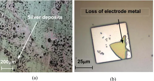
Fig. 3. (a) Silver deposits on the surface of the top insulator of the benchmark device after it was cycled between +0.5V and −0.5V for 10-15 minutes. (b) A microsquare electrode on a benchmark device, where a section of metal has detached after cycling for 5-10 minutes between+0.5V and−0.5V.
solvent limits of LKE [31]. The top insulator which defined the microelectrode and insulated the tungsten interconnect from the MS solution was also a 500 nm layer of Si-rich SiN.
Devices fabricated using this material combination were characterised by initially submerging them in LKE for half an hour at 500 °C after which they were removed and examined under a microscope. This showed no obvious signs of chemical attack (such as discolouration or surface damage). When potentials ranging between −1.5 V and +0.5 V were applied, the devices operated successfully, passing the currents associated with silver stripping (below −0.3V) and plating (above−0.3V) in the nA range for one to ten minutes, after which the currents increased markedly into the mA range. This increase in current was indicative of a failure in the top insula-tor leading to exposure of additional tungsten. Upon removal from LKE and inspection, it was found in these cases that the top insulation layer had delaminated, which was believed to have been caused by stress induced through electrochemical cycling. No delamination was observed when restricting the potential window to between −0.5 V and +0.5 V but the characteristic electrochemistry of silver plating and stripping could still be observed. However, it was also noticed that even in this reduced voltage window there were deposits of silver on the areas of the top insulator overlying the metal, as shown in figure 3(a), and the larger than expected currents persisted despite the absence of delamination events. Whilst restricting the operational voltage limits avoided delamination it indicated that the top insulator was ineffective in preventing the reduc-tion of silver ions at the underlying tungsten according to
Ag+(solv)+e−→Ag(s) (1)
Occasionally, in this restricted potential window, silver plating/stripping currents were also seen to decrease. When the device was removed from LKE and inspected, flakes of metal were missing from the microsquare as shown in figure 3(b). This implied there was also either poor adhesion between the layers or the electrode metal and/or the adhesion layer were becoming exposed to LKE and subsequently attacked leading to a reduction in the overall area of the tungsten.
In summary, the characterisation of the benchmark device highlighted the difficulties associated with performing
electrochemistry in LKE with these devices and presented the following series of challenges:
1. Delamination of the top insulator;
2. Susceptibility of the electrode metal to detachment; 3. The top insulator not operating as an effective barrier to
electrochemistry at the underlying metal.
In the following sections each of these failure mechanisms is analysed systematically and a solution to each mode of failure is presented. The end result is an optimised device capable of operating in the LKE environment. In the following sections it can be presumed unless stated otherwise that devices were evaluated by electrochemically cycling them over the voltage range−1.5 to+0.5 V.
B. Failure Analysis
1) Stress: The delaminations observed in the benchmark
device architecture indicated that excessive stress was being generated in the layered structure. There are two sources of the stress resulting from layer deposition; intrinsic (related to the internal structure of the film resulting from its deposition) and extrinsic (largely resulting from thermal-mismatch between layers). Depending on process conditions typically the intrinsic stress in Si-rich SiN is tensile and SiO2compressive [29] with
measured magnitudes of 375 ± 40MPa and 272 ± 34MPa respectively. These values agree with the literature [29] and were obtained using profilometry and the Stoney formula [32]. An example of a very successful stress relief strategy for the high level of intrinsic stress present in silicon nitride is the LOCOS process which is used for growing the field oxide in CMOS technology [33]. As noted above, SiO2has a
compres-sive stress and if this is matched with the tensile stress in the Si-rich layer SiN, wafer bow can be eliminated [29], [34]. This was consequently the approach used to relieve stress in the Si-rich SiN top insulator and thereby reduce the probability of delamination. Hence, devices were fabricated with a 500 nm thermally grown SiO2 layer in place of the 500 nm Si-rich
SiN base insulation layer used in the benchmark device. It was satisfying that when these devices were electrochemically cycled in the melt the stress levels were sufficiently reduced to the point where no delamination of the top SiN insulator layer was observed.
The extrinsic stress also needs to be considered and is mainly related to the thermal expansion mismatch between the deposited layer and the silicon substrate. In the electrodes fabricated in this paper it originates from the strain resulting from the wafer cooling to its room temperature dimensions after deposition. This bi-axial thermal mismatch stress is typically less than the intrinsic stress. Assuming the strain is set by the much thicker silicon wafer it can be calculated to be 84MPa for Si-rich SiN and 151MPa for SiO2for the wafer
operating at 500 °C.
Figure 4(a) and (b) compares devices fabricated with Si-rich SiN and SiO2 underlying insulators respectively after cycling
between −1.5 V and +0.5 V. It can be observed the stress relief provided by the underlying SiO2successfully reduces the
[image:4.612.51.300.58.189.2]Fig. 4. (a) Benchmark device with an Si-rich SiN underlying insulator where the top insulator has delaminated. (b) Device fabricated with a SiO2
underlying insulator which shows no delamination of the top insulator. The two devices were electrochemically cycled for 5 minutes at 500 °C.
Fig. 5. (a) Electrode with a strip of tungsten on a titanium adhesion layer where a large section of the titanium has been electrochemically stripped, removing the overlying tungsten. (b) A tungsten electrode with a titanium nitride adhesion layer which has been unaffected by electrochemical cycling.
However, it is also well known that silicon dioxide is chemically attacked by LKE. To confirm this, when a 500 nm film of thermally grown silicon dioxide was immersed in LKE, it was completely removed in under 10 minutes. Hence, an important design consideration is that the silicon dioxide underlying layer is either never directly exposed to LKE, or its exposure is limited so as to not impact on device lifetime.
2) Adhesion Layer: To investigate the effect of metal
detachment from the microsquare, a simple device consisting of a tungsten electrode metal film upon a titanium adhesion layer was connected and electrochemically cycled. In this case the electrochemical currents reduced to zero in under five minutes indicating loss of electrode metal. Figure 5(a) shows a sample following removal from the melt visually confirming this effect. As tungsten is a well-used electrode metal in LKE [30], it seems unlikely this was the source of the metal detachment. It was suspected that electrochemical dissolution of the underlying adhesion layer was responsible. To identify whether this was the case, a titanium wire was submerged into LKE and electrochemically cycled and was found to electrochemically dissolve at a potential of ∼0 V.
Fig. 6. Device fabricated with a Si3N4 top insulator following
electrochemical cycling at 500 °C for half an hour (left) and a magnified area of the surface showing no damage or silver deposition (right).
For the seed layer to be responsible for the electrode film removal, LKE must be able to reach the underlying titanium adhesion layer. The sporadic nature of this effect suggests it was most likely due to defects/pinholes in the electrode metal film. As pinholes are difficult to completely remove, it is advantageous to employ an adhesion layer which is not electrochemically dissolved by LKE over the required poten-tial range. Titanium nitride is known to offer good corrosion resistance and is an often used barrier material [35], [36]. To investigate the chemical and electrochemical response of deposited TiN in the salt, 20 nm of TiN was sputtered onto 500 nm of LPCVD Si-rich SiN and diced into strips. After being submerged in the salt, the TiN showed no signs of dissolution. The sample was then subjected to cyclic voltam-metry for 15 minutes at a sweep rate of 200 mVs−1. The titanium nitride was not electrochemically dissolved when cycled between −1.5 V and +0.5 V. Finally, to confirm the improved resistance of a combined tungsten metal layer and TiN adhesion layer to the salt, a device fabricated without a top insulator but with a 20 nm TiN adhesion layer and 200 nm tungsten layer was cycled in the melt for 30 minutes in the same potential window. The response was unchanged with time indicating resistance of the adhesion layer to electrochemical dissolution in LKE, as shown in figure 5(b). This confirmed that TiN was a suitable adhesion layer for these devices.
3) Top Insulator: It was observed that the Si-rich SiN top
insulator was not particularly robust and often failed to insulate successfully from the molten salt. It was possible that this was due to the Si-rich SiN not acting as an impermeable chemical barrier. It was expected that stoichiometric silicon nitride (Si3N4) would provide a better barrier to LKE than
[image:5.612.312.562.59.217.2]Si-rich SiN. This is because (a) Si-N bonds are more covalent in character than Si-Si bonds, making them more resistant to chemical attack, and (b) the material is denser than other SixNyratios [37].
Figure 6 shows a device with a Si3N4 top insulator after
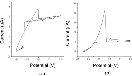
[image:5.612.66.285.281.427.2]Fig. 7. (a) CV of silver plating and stripping using benchmark electrode. (b) CV of silver plating and stripping using an optimised electrode.
It should be noted that stoichiometric Si3N4 has a
larger intrinsic tensile stress, which was measured to be 950 ±24MPa in agreement with literature values [29], [34]. Despite this increased tensile stress; the 500nm silicon dioxide continued to provide adequate stress relief and no delamination of the devices was observed. These devices also produced the desired quantitative electrochemical response, as reported in the next section.
VII. ELECTRODEPERFORMANCE- ELECTROCHEMICAL
CHARACTERISATION OFSILVER(I) CHLORIDE INLKE
After fabrication of the electrodes they were quantitatively characterised to identify fully functioning devices. To confirm the fabricated microelectrode was of the correct dimensions, the edge length was determined using the established expres-sion for the limiting current for a square microelectrode, which is given by [38]
iL =2.341n F DcL, (2)
where iL is the limiting current, n is the number of electrons
transferred, F is Faraday’s constant, D is the diffusion coef-ficient, c is the concentration of the redox agent and L is the microsquare edge length. The extraction of the expected edge length was considered to be a good indicator of a high-fidelity electrode and was used below for both the original benchmark device and the final optimised device, which incorporated the SiO2 underlying insulator, the TiN adhesion layer, and the
Si3N4 top insulator.
Figure 7(a) shows the cyclic voltammogram from a bench-mark electrode. It is important to note the high magnitude of the current and the disparity between charges passed during plating and stripping (often 5-10 times more current was passed in plating than stripping). The explanations for these two phenomena were silver plating on the metal areas underlying the top insulator and the subsequent isolation of deposited silver in the top insulator upon stripping. Both of these effects can be explained in terms of incomplete passivation by the top insulator. Using the established literature value of 2.42×10⁻⁵cm2s−1for the diffusion coefficient (D) of silver (I) chloride at 457 °C [39] in LKE and equation (2), the edge length calculated for the benchmark electrode in fig 7(a) was 6.6 mm. Such a large discrepancy between the defined microelectrode edge length (L =50 µm) and the
experimentally observed area was consistent with the Si-rich SiN providing incomplete passivation as previously discussed and illustrated in figure 3(a) and/or with delamination of the top insulator as shown in figure 4(a).
In contrast, figure 7(b) shows a cyclic voltammogram from an optimised electrode with L = 20 µm. The most immediate thing to note is that the current scale on figure 7(b) is now in the order of nA as opposed to µA in figure 7(a), which in itself is indicative of a microelectrode. Also evident in figure 7(b) is the sharp stripping peak and limiting current, arising from the diffusion-controlled mass transport, characteristic of microelectrodes. Using equation (2), an edge length of 19.6µm was calculated at 450 °C for the optimised electrode. This is a highly satisfying finding, as L is within 2% of the designed value, well within the tolerance reported for high fidelity ambient microelectrode systems [40]. This compares favourably with the electrodes in [10], where the electrode radius was determined electrochemically to be 40% larger than expected under ambient conditions. It should also be noted that the charge passed during silver plating was the same (0.7µC) as that passed during stripping. When this device was cycled using a range of scan rates, the electrochemical response also proved to be independent of scan rate further indicating that the device was performing as expected for a 20 µm square microelectrode. Finally, the device was cycled in the melt for 30 minutes with no change in the electrochemical response. Visual inspection after electrochemical cycling showed an unblemished top insulator film with tungsten metal still present in the previously defined electrode area. These analyses confirmed the successful production of working optimised devices overcoming the limitations identified in [7]–[19]. A more comprehensive electrochemical characterisation of these electrodes is presented in a companion publication [41].
VIII. DISCUSSION
Analysis of three key failure mechanisms provided an insight into the operation of microfabricated microelectrodes in the high temperature environment of LKE MS. This approach guided development of optimised devices that functioned in this environment for at least half an hour.
It has been shown that intrinsic stress is the most important stress related factor when operating in the LKE environment. In the role of underlying insulator; the Si-rich SiN layer con-tributes less thermal stress than the SiO2. However the intrinsic
stress is much higher and results in device delamination. There was a concern that dicing into individual chips exposed the SiO2 insulator to LKE along the cut edges. However no
detrimental effect has been observed over the time courses investigated to date.
The necessity of an electrochemically inert adhesion layer implies that there is infiltration of salt through the electrode metal, most likely via pinholes. For a robust device it is clear that the total performance of the material layers used must be considered, even if they are not in apparent direct contact with the salt.
The use of stoichiometric silicon nitride (Si3N4) as the
TABLE I
SUMMARY OFMATERIALCOMBINATIONSSTUDIED FORANALYSIS INMS
with the Si-rich SiN used in the previously reported process. Whilst the Si-rich SiN film had lower internal stress, when it is employed as the top insulator the measured currents are larger than expected as a result of incomplete passivation. This behaviour is not observed when a stoichiometric Si3N4
top insulator is employed. The dramatic improvement in passivation between the two silicon nitride layers also suggests it was not simply pinholes or defects in the top insulation layer, but the superior chemical resistance of Si3N4.
The engineering yield of the reported optimised devices is close to 100% and when left in the melt for two weeks with no electrical activation the devices appeared completely unaffected. As expected, when electrically activated, the device lifetime is heavily affected by the size of the potential window over which it was scanned and the temperature of the melt. A variation in electrode lifespan has been observed with the overwhelming majority of devices surviving between 0.5 hours and 2.5 hours of electrochemical activation when scanned between−1.5 V and+0.5 V. There have been a few device failures within 10 minutes and these short lifetimes are almost certainly due to latent defects. The failure rates can be further reduced by lowering particulate levels and in future devices tighter process controls are being implemented in order to improve operational lifetimes.
IX. CONCLUSION
This systematic study of layer material combinations for the manufacture of MS compatible microelectrodes has high-lighted a number of important issues and challenges. Effective stress relief is shown to prevent thin film delamination, use of an electrochemically inert adhesion layer prevents loss of electrode metal, and the use of stoichiometric silicon nitride as the top insulator provides effective passivation. The results of the material testing is summarised in table 1.
This paper has described the first microelectrode device capable of operating over extended periods in the chem-ically harsh environment of LKE at 500 °C. The impact of this technology is therefore highly suited to online monitoring in MS and with the prospect of pyrochemical processing of nuclear fuel becoming a widely adopted tech-nique, there is the potential for significant impact. We are currently developing sensors to enable real time monitoring for process control in flowing MS media and in stirred reaction vessels.
REFERENCES
[1] J.-C. Poignet and J. Fouletier, “Physico-chemical properties of molten salts,” in Materials Issues for Generation IV Systems, V. Ghetta, D. Gorse, D. Mazière, V. Pontikis, Eds. Berlin, Germany: Springer-Verlag, 2008, pp. 523–536.
[2] D. J. Fray, “Emerging molten salt technologies for metals production,”
J. Minerals, Metals Mater. Soc., vol. 53, no. 10, pp. 27–31, Oct. 2001.
[Online]. Available: http://link.springer.com/article/10.1007%2Fs11837-001-0052-5
[3] B. Mishra and D. L. Olson, “Molten salt applications in materials processing,” J. Phys. Chem. Solids, vol. 66, nos. 2–4, pp. 396–401, 2005. [4] M. Straka, L. Szatmáry, M. Marecek, and M. Korenko, “Uranium recov-ery from LiF–CaF2–UF4–GdF3system on Ni electrode,” J. Radioanal.
Nucl. Chem., vol. 298, no. 1, pp. 393–397, Oct. 2013. [Online].
Available: http://link.springer.com/article/10.1007%2Fs10967-013-2436-8
[5] A. Gil et al., “State of the art on high temperature thermal energy storage for power generation. Part 1—Concepts, materials and modellization,” Renew. Sustain. Energy Rev., vol. 14, no. 1, pp. 31–55, Jan. 2010. [Online]. Available: http://www.sciencedirect.com/ science/article/pii/S1364032109001774
[6] I. Yasuhiko and N. Toshiyuki, “Non-conventional electrolytes for electrochemical applications,” Electrochim. Acta, vol. 45, nos. 15–16, pp. 2611–2622, May 2000. [Online]. Available: http:// www.sciencedirect.com/science/article/pii/S0013468600003418 [7] M. R. Bermejo, J. Gómez, J. Medina, A. M. Martínez, and
Y. Castrillejo, “The electrochemistry of gadolinium in the eutec-tic LiCl–KCl on W and Al electrodes,” J. Electroanal. Chem., vol. 588, no. 2, pp. 253–266, Mar. 2006. [Online]. Available: http://www.sciencedirect.com/science/article/pii/S0022072806000350 [8] P. Baumli and G. Kaptay, “Wettability of carbon surfaces by pure molten
alkali chlorides and their penetration into a porous graphite substrate,”
Mater. Sci. Eng., A, vol. 495, nos. 1–2, pp. 192–196, 2008. [Online].
Available: http://www.kaptay.hu/pub/kaptay-j117.pdf
[9] S. Senderoff, “Electrode reactions in molten salts,” in Proc. Symp.
Electrochem. Process., 1967, pp. 32–36. [Online]. Available: https://web.anl.gov/PCS/acsfuel/preprint%20archive/11_1_MIAMI_04-67.htm
[10] B. Malinowska, M. Cassirl, and J. Devynck, “Design of a gold ultramicroelectrode for voltammetric studies at high temperature in glass-corrosive media (molten carbonate at 650 °C),” J. Electrochem.
Soc., vol. 141, no. 8, pp. 2015–2017, Aug. 1994. [Online]. Available:
http://jes.ecsdl.org/content/141/8/2015.full.pdf
[11] R. J. Forster and T. E. Keyes, “Behaviour of ultramicroelectrodes,” in Handbook of Electrochemistry, C. G. Zoski, Ed. Amsterdam, The Netherlands: Elsevier, 2007, pp. 155–171.
[12] M. Fleischmann and S. Pons, “The behavior of microelectrodes,” Anal.
Chem., vol. 59, no. 24, pp. 1391A–1399A, 1987.
[13] D. Pletcher, “Why microelectrodes?” in Microelectrodes: Theory and
Applications, I. Montenegro, M. A. Queirós, and J. L. Daschbach, Eds.
Norwell, MA, USA: Kluwer, 1991, pp. 3–15.
[14] K. Štulík, C. Amatore, K. Holub, V. Marecek, and W. Kutner, “Microelectrodes. Definitions, characterization, and applications,” Pure
Appl. Chem., vol. 72, no. 8, pp. 1483–1492, 2000. [Online]. Available:
http://pac.iupac.org/publications/pac/pdf/2000/pdf/7208x1483.pdf [15] M. J. Moorcroft, N. S. Lawrence, B. A. Coles, R. G. Compton,
and L. N. Trevani, “High temperature electrochemical studies using a channel flow cell heated by radio frequency radiation,” J. Electroanal.
Chem., vol. 506, no. 1, pp. 28–33, Jun. 2001. [Online]. Available:
http://www.sciencedirect.com/science/article/pii/S0022072801004685 [16] K. T. Chiang and L. Yang, “Development of crevice-free electrodes
for multielectrode array sensors for applications at high tempera-tures,” Corrosion, vol. 64, no. 10, pp. 805–812, Oct. 2008. [Online]. Available: http://www.nace.org/cstm/Store/Product.aspx?id=00950ecd-b924-dc11-94f4-0017a4466950
[17] K. T. Chiang, L. Yang, R. Wei, and K. Coulter, “Develop-ment of diamond-like carbon-coated electrodes for corrosion sen-sor applications at high temperatures,” Thin Solid Films, vol. 517, no. 3, pp. 1120–1124, Dec. 2008. [Online]. Available: http://www. sciencedirect.com/science/article/pii/S0040609008009887
[19] R. T. Carlin and R. A. Osteryoung, “Deposition studies of lithium and bismuth at tungsten microelectrodes in LiCl:KCl eutectic,”
J. Electrochem. Soc., vol. 136, no. 5, pp. 1249–1255, Jan. 1989. [Online].
Available: http://jes.ecsdl.org/content/136/5/1249.abstract
[20] H. Wang, N. J. Siambun, L. Yu, and G. Z. Chen, “A robust alumina membrane reference electrode for high temperature molten salts,”
J. Electrochem. Soc., vol. 159, no. 9, pp. H740–H746, 2012.
[Online]. Available: http://jes.ecsdl.org/content/159/9/H740?related-urls=yes&legid=jes;159/9/H740
[21] M. A. Py and R. R. Haering, “Structural destabilization induced by lithium intercalation in MoS2 and related compounds,”
Can. J. Phys., vol. 61, no. 1, pp. 76–84, 1983. [Online]. Available: http://www.nrcresearchpress.com/doi/abs/10.1139/p83-013#. VM9AU9LWKpc
[22] A. Relf, D. Corrigan, C. L. Brady, J. G. Terry, A. J. Walton, and A. R. Mount, “Robust microelectrodes in molten salt analysis,” ECS
Trans., vol. 50, no. 11, pp. 105–109, 2013. [Online]. Available:
http://ecst.ecsdl.org/content/50/11/105.abstract
[23] M. J. Madou, “Lithography,” in Fundamentals of Microfabrication, 2nd ed. Boca Raton, FL, USA: CRC Press, 2002, ch. 1, p. 1. [24] O. Hammerich, “Methods for studies of electrochemical reactions,” in
Organic Electrochemistry, 4th ed. New York, NY, USA: Marcel Dekker,
2001, ch. 2, p. 133.
[25] P. Masset, R. J. M. Konings, R. Malmbeck, J. Serp, and J.-P. Glatz, “Thermochemical properties of lanthanides (Ln=La, Nd) and actinides (An = U, Np, Pu, Am) in the molten LiCl–KCl eutectic,” J. Nucl.
Mater., vol. 344, nos. 1–3, pp. 173–179, 2005. [Online]. Available:
http://www.sciencedirect.com/science/article/pii/S0022311505002217 [26] Y.-L. Liu et al., “Electrochemical extraction of samarium
from LiCl-KCl melt by forming Sm-Zn alloys,” Electrochim. Acta, vol. 120, pp. 369–378, Feb. 2014. [Online]. Available: http://www.sciencedirect.com/science/article/pii/S0013468613025218 [27] M. Mohamedi, N. Kawaguchi, Y. Sato, and T. Yamaura,
“Electrochemical study of the mechanism of formation of the surface alloy of aluminum–niobium in LiCl–KCl eutectic melt,” J. Alloys
Compounds, vol. 287, nos. 1–2, pp. 91–97, 1999. [Online]. Available:
http://www.sciencedirect.com/science/article/pii/S0925838899000201 [28] T. L. Chu, C. H. Lee, and G. A. Gruber, “The preparation and
properties of amorphous silicon nitride films,” J. Electrochem. Soc., vol. 114, no. 7, pp. 717–722, 1967. [Online]. Available: http://jes.ecsdl. org/content/114/7/717.abstract
[29] D. Flandre, J. Laconte, and J.-P. Raskin, “Thin dielectric films stress extraction,” in Micromachined Thin-Film Sensors for SOI-CMOS Co-Integration. Berlin, Germany: Springer-Verlag, 2006, ch. 2, pp. 47–103. [Online]. Available: http://link.springer. com/chapter/10.1007/0-387-28843-0_3
[30] M. J. Madou, “Pattern transfer with additive techniques,” in
Fundamen-tals of Microfabrication, 2nd ed. Boca Raton, FL, USA: CRC Press,
2002, ch. 3, p. 126.
[31] M. Misra, K. S. Raja, and J. Ruppert, “Electrochemical corro-sion behavior of refractory metals in LiCl-Li2O molten salt,” ECS
Trans., vol. 33, no. 7, pp. 181–192, 2010. [Online]. Available:
http://ecst.ecsdl.org/content/33/7/181.abstract
[32] M. Zecchino and T. Cunningham, Thin Film Stress Measurement
Using Dektak Stylus Profilers. Plainview, NY, USA: Veeco, 2004. [Online]. Available: http:/www.rpi.edu/dept/cie/mncr/ documents/AN516_Dektak_Stress_Measure.pdf
[33] J. P. Uyemura, “Fabrication and layout of CMOS integrated circuits,” in
CMOS Logic Circuit Design. Norwell, MA, USA: Kluwer, 2001, ch. 2,
sec. 2.4.1, pp. 74–77.
[34] O. Zohni, G. Buckner, T. Kim, A. Kingon, J. Maranchi, and R. Siergiej, “Investigating thin film stresses in stacked silicon dioxide/silicon nitride structures and quantifying their effects on frequency response,”
J. Micromech. Microeng., vol. 17, no. 5, pp. 1042–1051, 2007. [Online].
Available: http://iopscience.iop.org/0960-1317/17/5/026
[35] K. Hai, T. Sawase, H. Matsumura, M. Atsuta, K. Baba, and R. Hatada, “Corrosion resistance of a magnetic stainless steel ion-plated with tita-nium nitride,” J. Oral Rehabil., vol. 27, no. 4, pp. 361–366, Apr. 2000. [Online]. Available: http://www.ncbi.nlm.nih.gov/pubmed/10792599 [36] D. Starosvetsky and I. Gotman, “Corrosion behavior of titanium
nitride coated Ni-Ti shape memory surgical alloy,” Biomaterials, vol. 22, no. 13, pp. 1853–1859, 2001. [Online]. Available: http://www. ncbi.nlm.nih.gov/pubmed/11396890
[37] B. K. Yen et al., “Microstructure and properties of ultrathin amorphous silicon nitride protective coating,” J. Vac. Sci. Technol. A, Vac., Surf.,
Films, vol. 21, no. 6 pp. 1895–1904, Nov. 2003. [Online]. Available:
http://www.slac.stanford.edu/cgi-wrap/getdoc/slac-pub-10008.pdf
[38] H. L. Woodvine, J. G. Terry, A. J. Walton, and A. R. Mount, “The development and characterisation of square microfabricated electrode systems,” Analyst, vol. 135, no. 5, pp. 1058–1065, May 2010. [Online]. Available: http://www.ncbi.nlm.nih.gov/pubmed/20419257
[39] G. J. Janz and N. P. Banal, “Molten salts data: Diffusion coeffi-cients in single and multi-component salt systems,” J. Phys. Chem.
Ref. Data, vol. 11, no. 3, pp. 505–693, 1982. [Online]. Available:
http://scitation.aip.org/content/aip/journal/jpcrd/11/3/10.1063/1.555665 [40] M. Sosna, G. Denuault, R. W. Pascal, R. D. Prien, and M.
Mowlem, “Development of a reliable microelectrode dissolved oxygen sensor,” Sens. Actuators B, Chem., vol. 123, no. 1, pp. 344–351, 2007. [Online]. Available: http://www.sciencedirect.com/science/article/ pii/S0925400506006083
[41] D. K. Corrigan, E. O. Blair, J. G. Terry, A. R. Mount, and A. J. Walton, “Enhanced electroanalysis in lithium potassium eutectic (LKE) using microfabricated square microelectrodes,” Anal. Chem., vol. 86, no. 22, pp. 11342–11348, Nov. 2014. [Online]. Available: http://pubs.acs.org/doi/abs/10.1021/ac5030842
Ewen O. Blair received the M.A. (Hons.) degree in physics and philosophy from the University of Aberdeen, Aberdeen, U.K., in 2012. He is cur-rently pursuing the Ph.D. degree in fabrication and optimization of durable electrochemical sensors for molten salts on the EPSRC funded by the REFINE project.
He was involved in the characterization of novel photoconductive materials during his time with the University of Aberdeen.
Damion K. Corrigan is currently a PDRA with the School of Chemistry, University of Edinburgh, Edinburgh, U.K. His research experience lies mainly in the areas of electrochemical and optical sensing technologies. He has spent two years with the Division of Pathway Medicine, Edinburgh Royal Infirmary, Edinburgh, under the co-supervision of Prof. Mount, working on the development of a point of care compatible electrochemical sensor for the rapid detection of MRSA.
He was with the Electrochemistry Group, University of Southampton, Southampton, U.K., where he was involved in a project using microstructured electrodes for the optical detection and electrochemical discrimination of DNA sequences, before moving to Edinburgh. He received the Ph.D. degree in bioanalytical chemistry from Cranfield University, Bedford, U.K., which was funded by GSK, and was involved in the development of sensor systems to address specific purity problems associated with large-scale pharmaceutical manufacture. His first post-doctoral position (funded by GSK and in collaboration with GSK Barnard Castle Plant) was a continuation of the work undertaken during his Ph.D.
Jonathan G. Terry (SM’08) received the B.Eng. degree in electronics engineering, the M.Sc. degree in microelectronic material and device technology, and the Ph.D. degree in solid-state electronics from the University of Manchester Institute of Science and Technology, Manchester, U.K. He joined the Institute for Integrated Micro and Nanosystems, University of Edinburgh, Edinburgh, U.K., in 1999, as a Research Fellow. He is currently a Chancellor’s Fellow and Lecturer with the University of Edinburgh, where his main area of interest is in the development of More-than-Moore technologies, and the integration of novel fabrication processes and materials with foundry CMOS to create smart microsystems.
His work received a number of awards, including the IEEE International Conference on Microelectronic Test Structures Best Paper Award in 2004, the IET Nanobiotechnology Premium Award in 2008, and the International
Journal of Molecular Sciences Best Paper Award in 2013. He has over
Andrew R. Mount is currently a Professor and the Head of Physical Chemistry with the University of Edinburgh, Edinburgh, U.K. He was the Royal Soci-ety of Edinburgh/SEELLD Support Research Fellow. He has authored over 70 papers and holds 10 patents. He has interests and expertise in electrochemical production, and the combination of spectroscopic (in particular, fluorescence) and electrochemical characterization.
He has collaborated with the National Nuclear Laboratory, Cumbria, U.K., for the last 10 years, as an Electrochemical Consultant on electroanalysis in room and high temperature molten salt systems. During this period, he has also been a Principal Investigator and an active member of the management team in over £9M of successful multidisciplinary projects to develop optical and electrochemical sensors and devices, directly supervising six PDRAs and involving dual and multisite supervision. He is the Chair of the RSC Electrochemistry Group; a member of the RSC Faraday Standing Committee on Conferences; the Founding Member of the Centre for Materials Science, Edinburgh; the Edinburgh Materials Microanalysis Centre, Edinburgh; and the Centre for Science at Extreme Conditions, Edinburgh; and a reviewer with the Oak Ridge National Laboratory, Oak Ridge, TN, USA. He was the Chair of the Faraday Discussion 149 (2010).
Anthony J. Walton (SM’88) is currently a Professor of Microelectronic Manufacturing with the School of Engineering, University of Edinburgh, Edinburgh, U.K. Over the past 25 years, he has been actively involved with the semiconductor industry in a number of areas associated with silicon processing that includes both integrated circuit technology and microsystems. In particular, he has been intimately involved in the development of technologies and their integration with CMOS. He played a key role in setting up the Scottish Microelectronics Centre, Edinburgh, which is a purpose-built facility for research and development and commercialization. He has authored over 350 papers.
He has received best paper awards from the IEEE TRANSACTIONS ON
SEMICONDUCTORMANUFACTURING, the Proceedings of the International
Society of Hybrid Manufacturers, the International Journal of Molecular Sciences, and the IEEE International Conference on Microelectronic Test
Structures (ICMTS), and received the IET Nanobiotechnology Premium Award. He is a Fellow of the Royal Society (Edinburgh). He served as the Chairman for a number of conferences, including the European Solid-State Devices Research Conference in 1994 and 2008, and ICMTS in 1989 and 2008. He serves on numerous technical committees. He is an Associate Editor of the IEEE TRANSACTIONS ON SEMICONDUCTOR