This is a repository copy of
Characterisation of Al0.52In0.48P mesa p-i-n photodiodes for
X-ray photon counting spectroscopy
.
White Rose Research Online URL for this paper:
http://eprints.whiterose.ac.uk/105906/
Version: Accepted Version
Article:
Butera, S., Lioliou, G., Krysa, A.B. orcid.org/0000-0001-8320-7354 et al. (1 more author)
(2016) Characterisation of Al0.52In0.48P mesa p-i-n photodiodes for X-ray photon
counting spectroscopy. Journal of Applied Physics, 120 (2). 024502. ISSN 0021-8979
https://doi.org/10.1063/1.4956153
This is the accepted version of the following article: Journal of Applied Physics, 120,
024502 (2016), which has been published in final form at
http://dx.doi.org/10.1063/1.4956153.
eprints@whiterose.ac.uk https://eprints.whiterose.ac.uk/ Reuse
Unless indicated otherwise, fulltext items are protected by copyright with all rights reserved. The copyright exception in section 29 of the Copyright, Designs and Patents Act 1988 allows the making of a single copy solely for the purpose of non-commercial research or private study within the limits of fair dealing. The publisher or other rights-holder may allow further reproduction and re-use of this version - refer to the White Rose Research Online record for this item. Where records identify the publisher as the copyright holder, users can verify any specific terms of use on the publisher’s website.
Takedown
If you consider content in White Rose Research Online to be in breach of UK law, please notify us by
Characterisation of Al
0.52In
0.48P mesa p-i-n photodiodes for
X-ray photon counting spectroscopy
S. Butera1a), G. Lioliou1, A. B. Krysa2, A.M. Barnett1
1
Semiconductor Materials and Device Laboratory, School of Engineering and
Informatics, University of Sussex, Brighton, BN1 9QT, UK.
2
EPSRC National Centre for III-V Technologies, University of Sheffield, Mappin
Street, Sheffield, S1 3JD, UK.
Results characterising the performance of thin (2 m i-layer) Al0.52In0.48P p+-i-n+ mesa
photodiodes for X-ray photon counting spectroscopy are reported at room
temperature. Two 200 m diameter and two 400 m diameter Al0.52In0.48P p+-i-n+
mesa photodiodes were studied. Dark current results as a function of applied reverse
bias are shown; dark current densities < 3 nA/cm2 were observed at 30 V (150 kV/cm)
for all the devices analysed. Capacitance measurements as a function of applied
reverse bias are also reported. X-ray spectra were collected using 10 s shaping time,
with the device illuminated by an 55Fe radioisotope X-ray source. Experimental
results showed that the best energy resolution (FWHM) achieved at 5.9 keV was
930 eV for the 200 m Al0.52In0.48P diameter devices, when reverse biased at 15 V.
System noise analysis was also carried out and the different noise contributions were
computed.
I. INTRODUCTION
Wide bandgap photodetectors may play a very important role in aerospace and
military applications; since they present lower leakage currents [1, 2] than alternative
narrower bandgap materials, such as silicon or germanium, they can operate at room
temperature and above without cooling system [3, 4]. Consequently, they potentially
offer cheaper and more compact technologies that may be useful in space missions [5]
and terrestrial applications outside the laboratory environment [6] requiring X-ray
spectroscopy. X-ray photon counting spectroscopy has been demonstrated using
different wide bandgap semiconductors: high-resolution X-ray spectra have already
been achieved, even at high temperature, using SiC, GaAs and AlGaAs detectors.
Bertuccio et al. [3] reported X-ray spectroscopy, over the temperature range 30 °C to
100 °C, using a SiC X-ray detector. Energy resolutions (FWHM) at 5.9 keV of
196 eV and 233 eV were observed at 30 °C and 100 °C, respectively. Another
material that can be used in X-ray spectroscopy is GaAs. Barnett et al. demonstrated
2 m thick GaAs p+-i-n+ mesa X-ray photodiodes, at temperatures from -30 °C to
80 °C, with energy resolutions at 5.9 keV of 800 eV and 1.5 keV at 20 °C and 80 °C,
respectively [4]; whilst Lioliou et al. reported 7 m thick GaAs p+-i-n+ mesa X-ray
photodiodes with energy resolutions at 5.9 keV of 750 eV at 20 °C [2]. At 23 °C, an
energy resolution as low as 266 eV was achieved using GaAs detectors by Owens et
al. [7]. Al0.8Ga0.2As photodiodes have been also demonstrated by Barnett et al. [8] to
operate as photon counting spectroscopy X-ray detectors over the temperature ranges
-30 °C to 90 °C, energy resolutions at 5.9 keV of 1.07 keV and 2.2 keV were
observed at room temperature and at 90 °C, respectively, limited by the noise of the
preamplifier used.
Another material usually used to produce efficient detection systems for soft and hard
X-rays, as well as -rays, is CdTe [9] CdTe and its related compounds (e.g. CdZnTe,
CdMnTe) can be used for radiation detection at different temperatures. At -60 C°,
energy resolutions (FWHM) of 310 eV and 600 eV at 5.9 keV and 59 keV,
respectively, were reported using CdTe detector [10]; at -37 °C, FWHM of 311 eV
and 824 eV at 5.9 keV and 59 keV, respectively, were demonstrated for a CdZnTe
detector [11]. These compounds can also operate at increased temperatures, albeit
with degraded energy resolution: for example, 53 keV (FWHM) at 122 keV was
observed for CdTe at 92 °C [12], whilst a 9.4 keV (FWHM) at 32 keV was reported
for CdZnTe at 70 °C [13]. CdTe and CdZnTe are attractive choices for producing
large area radiation detectors and for this reason they have received considerable
research attention [14]; spectroscopic CdZnTe and CdTe detector imaging arrays, for
example, have been proven by Wilson et al. [15].
A III-V wide bandgap ternary compound that could be very useful for radiation
detection at high temperatures is Al0.52In0.48P [16]. Al0.52In0.48P can be beneficial in
X-ray energies: AlInP structures, with an appropriate thick charge collection layer,
can be used to detect hard X-rays, as well as soft X-ray photons. The use of
Al0.52In0.48P for X-ray spectroscopy is a new research field that can provide innovative
X-ray systems with high-energy resolution [17]. Al0.52In0.48P has an indirect bandgap
of 2.31 eV [18], and it is nearly lattice matched with GaAs. Al0.52In0.48P is widely
used in semiconductor optoelectronics and the crystalline quality of the nearly lattice
matched Al0.52In0.48P can be very high in comparison to III-V nitrides, IV and II-VI
compounds of a similar bandgap. The doping in Al0.52In0.48P is also easier to control
than in some II-VI semiconductors. This paper reports initial characterisation of
Al0.52In0.48P p+-i-n+ mesa photodiodes for X-ray photon counting spectroscopy. For
the first time, a non-avalanche Al0.52In0.48P photodiode was used in a spectrometer and
a system energy resolution of 930 eV at 5.9 keV for a 200 m device observed; these
significant results have been achieved because of the high performances of the
Al0.52In0.48P detector used and the custom low-noise charge sensitive preamplifier
electronics developed at our laboratory. The Al0.52In0.48P device is the thickest i-layer
mesa Al0.52In0.48P detector produced so far, highlighting the advanced growth and
fabrication technologies used.
II. DEVICE STRUCTURE
The Al0.52In0.48P epilayer of the device was grown by metalorganic vapour phase
epitaxy (MOVPE) on a commercial (100) n-GaAs: Si substrate with a misorientation
of 10 degrees towards <111>A to suppress the CuPt-like ordered phase. The doping
concentrations of the Al0.52In0.48P p and n layers were 5 1017 cm-3 and 2 1018 cm-3,
respectively. The layers’ thicknesses were 0.2 m for the p+-region, 2 m for the
i-region and 0.1 m for the n+-region. After growth, the wafer was processed to form
mesa structures using 1:1:1 H3PO4: H2O2: H2O solution followed by 10 s in 1:8:80
H2SO4: H2O2: H2O solution. Unpassivated 200 m and 400 m diameter Al0.52In0.48P
mesa photodiodes were produced. An Ohmic rear contact consisting of 20 nm of InGe
and 200 nm of Au was evaporated onto the rear of the substrate and an Ohmic top
contact consisting of 20 nm of Ti and 200 nm of Au was evaporated on the p-side of
the mesa device. The top Ohmic contact had an annular shape; it covered 33% and
The device layers, their relative thicknesses and materials are summarised in
TABLE I.
TABLE I. Layer details of the Al0.52In0.48P photodiode. Layer Material Thickness
( m)
Dopant Dopant Type
Doping density (cm-3)
1 Ti 0.02
2 Au 0.2
3 GaAs 0.01 Zn p+ 1 1019
4 Al0.52In0.48P 0.2 Zn p+ 5 1017
5 Al0.52In0.48P 2 undoped
6 Al0.52In0.48P 0.1 Si n+ 2 1018 7 Substrate n+ GaAs
8 Au 0.2
9 InGe 0.02
Using the Beer-Lambert law and assuming complete charge collection in the p-, i- and
n- layers, X-ray quantum efficiencies (QE) through the device optical window (region
not covered by contacts) were calculated as a function of photon energy up to 10 keV
for the Al0.52In0.48P p+-i-n+ mesa photodiodes, Fig. 1.
[image:5.612.59.484.349.695.2]
Fig.1. Calculated quantum efficiency of Al0.52In0.48P p+-i-n+ mesa photodiodes as a function of photon energy. The discontinuities shown correspond to the Aluminium and Phosphorus K X-ray edges and Indium L X-ray edge.
X-ray quantum efficiencies (QE) of 22% and 18% were calculated for the device for
5.9 keV and 6.49 keV photons, respectively. The Al0.52In0.48P attenuation coefficients
at 5.9 keV and 6.49 keV were estimated [19, 20] to be 0.1109 m-1 and 0.0856 m-1.
The attenuation coefficients at 5.9 keV and 6.49 keV in Al0.52In0.48P are higher than
m-1, respectively [21]) and Al0.8Ga0.2As (0.0788 m-1 and 0.0604 m-1, respectively
[20]).
III. EXPERIMENTAL RESULTS
A. Electrical characterisation: Current-Voltage and Capacitance-Voltage measurements
Two 200 m diameter (D1 and D2) and two 400 m diameter (D3 and D4)
Al0.52In0.48P photodiodes were investigated at room temperature in a dry nitrogen
atmosphere (relative humidity <5%). The devices studied were randomly selected
from those available and were unpassivated.
Dark current characteristics as functions of applied bias were measured. Reverse bias
measurements from 0 V to 30 V were made in 1 V increments using a computer
controlled Keithley 6487 picoammeter/voltage source. The uncertainty associated
with the current readings was 0.3% of their values plus 400 fA, while the uncertainty
associated with the applied biases was 0.1% of their values plus 1 mV [22]. Dark
current densities < 3 nA/cm2 were observed at 30 V (150 kV/cm) for all the devices
analysed. These values are comparable with previously reported high quality
Al0.52In0.48P p+-i-n+ photodiodes having 1.03 m i-layer thickness [23]. The reported
leakage current was lower than GaAs (1.08 nA/cm2 at 22 kV/cm) [2] and Al0.8Ga0.2As
(4.72 nA/cm2 at 29 kV/cm) [24] detectors at similar electric fields and temperatures.
The Al0.52In0.48P dark current density was greater than for some previously reported
SiC detectors (1 pA/cm2 at 103 kV/cm) [3] at similar electric field and temperatures.
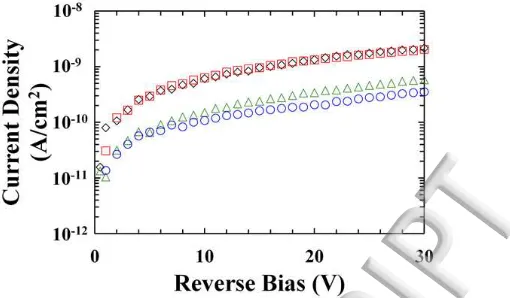
Fig. 2 shows the dark current density as a function of reverse bias for the presently
reported Al0.52In0.48P photodiodes. The different sized devices had different leakage
current density, indicating that surface leakage current was significant in the analysed
photodiodes. In a mesa photodiode, the dark current consists of a bulk leakage
contribution, which is proportional to the mesa area, and the surface leakage
contribution, which is proportional to the mesa perimeter [25, 26]. If the surface
leakage current is negligible, the current density for different sized devices should be
constant; consequently if current densities don’t match across diodes of different size,
Fig. 2. Dark current density as a function of applied reverse bias at room temperature for Al0.52In0.48P devices. Empty rhombuses (black) and empty squares (red) referred to data taken on the two 200 m diameter devices, D1 and D2 respectively; empty circles (blue) and empty triangles (green) referred to data taken on the two 400 m diameter devices, D3 and D4, respectively. Colour only available in the online version.
The depletion depths and the doping concentrations in the intrinsic regions of the
devices were calculated from capacitance measurements at room temperature. The
capacitance was measured as a function of applied reverse bias, between 0 V and
20 V, using an HP 4275A Multi Frequency LCR meter. The test signal was sinusoidal
with a 50 mV rms magnitude and 1 MHz frequency. The capacitance of an identical
empty package was also measured, 0.77 pF ± 0.02 pF, and subtracted from the
measured capacitance of the packaged photodiodes to determine the capacitance of
the devices themselves. The uncertainty associated with each capacitance reading was
0.12% [27]; while the uncertainty associated with the applied biases was 0.1% of
their values plus 1 mV. Fig. 3a and Fig. 3b show the capacitance as a function of
applied reverse bias for the 200 m and 400 m diameter devices, respectively. The
variations in the capacitance values between diodes of same diameters were within
Fig. 3. Capacitance as a function of applied reverse bias at room temperature (a) for the 200 m diameter Al0.52In0.48P devices, D1 (blue empty rhombuses) and D2 (red empty squares), and (b) for the 400 m diameter Al0.52In0.48P devices, D3 (blue empty circles) and D4 (red empty triangles). Colour only available in the online version.
For each diode analysed, the depletion depth (W) was calculated by:
where 0 is the permittivity of the vacuum, r is the Al0.52In0.48P dielectric constant
(11.25 [23]), and A is the device area [28].
Fig. 4a and Fig. 4b show the depletion depth as a function of applied reverse bias for
the 200 m and 400 m diameter devices, respectively.
Fig. 4. Depletion depth as a function of applied reverse bias at room temperature (a) for the 200 m diameter Al0.52In0.48P devices, D1 (red empty rhombuses) and D2 (blue empty squares), and (b) for the 400 m diameter Al0.52In0.48P devices, D3 (red empty circles) and D4 (blue empty triangles). Colour only available in the online version.
The application of the reverse bias to the diode increased the depth of the depletion
region. At reverse bias bigger than 5 V, the depletion region approached the n-layer
and increased more slowly due to the higher doping concentration in the doped
regions. The measured discrepancy in depletion depth at 20 V between the 200 m
and 400 m devices was smaller than its uncertainty, which was calculated to be
(0.08 ± 0.17) m.
where 0 is the permittivity of the vacuum, r is the Al0.52In0.48P dielectric constant
(11.25 [23]), and A is the device area [28]. Fig. 5 is an example of the determined
doping carrier concentration calculated as a function of depletion depth, in this
particular case the results from one of the 400 m diameter devices are presented;
similar results, as expected, were obtained for the other samples characterised. The
doping density in the i-layer was found to be (4.3 ± 0.7) × 1016 cm-3 this value
[image:9.612.66.508.120.701.2]increased to (3.5 ± 0.4) × 1017 cm-3 at i-n interface.
Fig. 5. Doping concentration below the p+-i junction as a function of depletion depth at room temperature for 400 m diameter Al0.52In0.48P device (D3).
B. X-ray spectroscopy and noise analysis
At different applied biases, X-ray spectra were collected using the 200 m and 400
m diameter devices. An 55Fe radioisotope X-ray source (Mn K = 5.9 keV,
Mn K = 6.49 keV) was positioned 5 mm above the top of the Al0.52In0.48P mesa
photodiodes. Each diode in turn was connected to a custom-made, single channel,
charge sensitive preamplifier of feedback resistorless design [29]. The output from the
preamplifier was connected to an Ortec 572a shaping amplifier and then to a
multichannel analyser (MCA). The shaping time was 10 s and the live time limit for
each accumulated spectrum was 1000 s. The experiment was performed at room
accumulated with each diode reverse biased at 0 V, 5 V, 10 V and 15 V. As the
applied reverse bias was increased, an improvement in energy resolution (as
quantified by the FWHM at 5.9 keV) was observed, this was attributed to less charge
trapping noise at greater electric field strengths as the effects of reduced capacitance
were negligible. Fig. 6 shows an X-ray spectrum obtained at 15 V using a 200 m
diameter device. The counts of the zero energy noise peak of the preamplifier were
limited by setting the MCA’s low energy threshold to appropriate energy cut-off
values (2.67 keV) after the position of the zero energy peak had been established.
The 55Fe photopeak observed was the combination of the Mn K and Mn K lines at
5.9 keV and 6.49 keV, respectively. In Fig. 6, the fitted Gaussians representing the
Mn K and Mn K peaks are shown: the fittings took into account the relative X-ray
emission rates of the 55Fe radioisotope X-ray source at 5.9 keV and 6.49 keV in the
appropriate ratio [30] and the relative difference in efficiency of the detector at these
X-ray energies.
Fig. 6. 55Fe X-ray spectrum accumulated at 15 V reverse bias using 200 m diameter Al0.52In0.48P device (D2) at room temperature. The shaping time used is 10 s. Also shown are the fitted Mn K (blue dashed line) and Mn K (red dashed-dot line) peaks. Colour only available in the online version.
An energy resolution (FWHM) at 5.9 keV of 930 eV was measured for both the 200
m diameter Al0.52In0.48P devices studied. The FWHM at 5.9 keV was 1.2 keV for
both the 400 m diameter Al0.52In0.48P devices.
The energy resolution (FWHM) of non-avalanche X-ray photodiode spectrometers is
noise [31]. The Fano noise is due to the statistical nature of the impact ionisation
process. If the electron-hole pair creation energy ( ) in Al0.52In0.48P was 5.8 eV (2.5
times the bandgap) and the Fano factor (F), using a conservative assumption, 0.12, the
likely Fano noise was estimated to be 151 eV FWHM at 5.9 keV. It should be noted
that measurements of the electron-hole pair creation energy and the Fano factor are
yet to be reported for Al0.52In0.48P. Knowledge of and F and their temperature
dependences is important because they in part determine the statistically limited
spectral resolution of an X-ray detector. The electronic noise consists of parallel white
noise, series white noise, 1/f noise and dielectric noise [32, 33]. The parallel white
noise takes into account the leakage currents of the detector and input JFET of the
preamplifier, whilst the series white noise takes into account the capacitances of the
detector and input JFET of the preamplifier. The parallel white noise, series white
noise, 1/f noise were calculated for the reported detectors. The series white noise
contribution was adjusted for induced gate current noise [34]. Each noise contribution
was found to be similar for devices with same diameter, Fig. 7 shows the parallel
white noise, series white noise and 1/f noise values as a function of reverse bias for
[image:11.612.61.500.330.705.2]200 m diameter (a) and 400 m diameter (b) devices.
Fig. 7. Equivalent noise charge as a function of applied reverse bias at room temperature using (a) 200 m diameter Al0.52In0.48P device, D1, and (b) 400 m diameter device D3. In both graphs, the parallel white noise (red empty squares), the series white noise (blue empty circles) and the 1/f noise (green empty triangles) contributions are shown. Colour only available in the online version.
At every applied reverse bias, the parallel white noise values were very similar
between all the diodes under analysis; this was due to similar leakage currents
(maximum 0.3 pA at 15 V). In both the 400 m diameter devices the series white
noise and the 1/f noise values, instead, were bigger with respect to the 200 m
higher device capacitance. Charge trapping noise is due to incomplete charge
collection. The combined contribution of the dielectric noise and charge trapping
noise at 5.9 keV was calculated by subtracting in quadrature the Fano noise, parallel
white noise, series white noise and 1/f noise contributions at 5.9 keV from the
measured FWHM at 5.9 keV. The computed combined dielectric and trapping noise
[image:12.612.192.482.159.374.2]contributions at 5.9 keV are reported in Fig. 8.
Fig. 8. Equivalent noise charge of the dielectric and trapping noise contribution at 5.9 keV as a function of applied reverse bias at room temperature. Empty circles (blue) and empty triangles (red) refer to the calculated dielectric and trapping noise at 5.9 keV on the two 200 m diameter devices, D1 and D2 respectively; empty rhombuses (green) and empty squares (black) refer to the calculated dielectric and trapping noise at 5.9 keV of the two 400 m diameter devices, D3 and D4 respectively. Colour only available in the online version.
For all the photodiodes analysed, the dielectric and trapping noise contribution at
5.9 keV is bigger at 0 V than at higher voltages. This is due to the great trapping noise
at 0 V. At increased reverse bias, the charge transport improved resulting in less
trapping noise. Since the dielectric noise is expected to be independent of reverse bias
[31], the reduction in equivalent noise charge (ENC) shown in Fig. 8 can be attributed
to reductions in charge trapping noise as a consequence of improved charge transport
at higher electric fields. For the 200 µm and 400 µm diameter diodes, when the
reverse bias was increased from 10 V to 15 V, the charge trapping noise reduced by
18 e- rms ENC and 34 e- rms ENC, respectively. These contributions were small
compared with the other noise sources.
photodiodes is worse than the spectral resolutions at 5.9 keV observed by Bertuccio et
al. [3] for SiC detectors (196 eV) and Owens et al. [7] for GaAs detectors (266 eV),
largely this can be attributed to the lower electronic noise associated with their
device’ readout electronics and also the extremely high quality materials used. In the
presently reported Al0.52In0.48P study, device readout electronics similar to Lioliou et
al. [2] and Barnett et al. [8] were used. The energy resolutions achieved with the
present Al0.52In0.48P detectors are slightly poorer than those reported with GaAs
(750 eV) by Lioliou et al. [2] but better than those reported with Al0.8Ga0.2As
(1.07 eV) by Barnett et al. for Al0.8Ga0.2As [8]. Al0.52In0.48P detectors are performing
better than Al0.8Ga0.2As detectors at room temperature; this is interesting since the
optimum bandgap for the room temperature operation (1.5 eV [35, 36]) is closer to
the Al0.8Ga0.2As bandgap (2.09 eV) than that of Al0.52In0.48P (2.31 eV). This may be
an indication of a lower than expected electron-hole pair creation energy in
Al0.52In0.48P or smaller charge trapping noises in Al0.52In0.48P.
III. CONCLUSION
In this paper, results characterising prototype non-avalanche Al0.52In0.48P p+-i-n+ mesa
X-ray photodiodes were investigated as detectors for X-ray photon counting
spectroscopy at room temperature using an 55Fe radioisotope X-ray source. Initial
dark current and capacitance measurements as functions of applied reverse bias are
reported for 400 m diameter and 200 m diameter devices. Dark current densities <
3 nA/cm2 were observed at 30 V for all the Al0.52In0.48P devices. At 0 V, capacitances
of 6.5 pF and 1.7 pF were observed for the 400 m diameter and 200 m diameter
devices, respectively. 55Fe X-ray spectra were collected using the devices. The results
showed that the best energy resolution at 5.9 keV, 930 eV FWHM, was achieved at a
reverse bias of 15 V for the 200 m diameter devices. The FWHM at 5.9 keV was 1.2
keV for both the 400 m diameter Al0.52In0.48P devices under the same conditions.
System noise analyses showed that the series white and the 1/f noises were bigger in
the 400 m diameter devices with respect to the 200 m diameter devices, this was
due to the higher capacitance. The parallel white noise was also computed and it was
similar between all the diodes under analysis; this was due to similar leakage currents.
The main source of noise limiting the energy resolution of the reported system was
reverse biases > 0 V, the charge transport improved resulting in less trapping noise
and corresponding better energy resolution.
ACKNOWLEDGMENTS
This work was supported by STFC grants ST/M002772/1 and ST/M004635/1
(University of Sussex, A. M. B., PI) and Royal Society Grant RS130515 (University
of Sussex, A. M. B., PI). The authors are grateful to R. J. Airey and S. Kumar at the
EPSRC National Centre for III-V Technologies for device fabrication. G. Lioliou
acknowledges funding received from University of Sussex in the form of a PhD
scholarship.
REFERENCES
1
G. Lioliou, M. Mazzillo, A. Sciuto, and A. M. Barnett, Opt. Express 23, 21657 (2015).
2
G. Lioliou, X. Meng, J. S. Ng, and A. M. Barnett, Nucl. Instrum. Meth. Phys. Res., Sect. A 813, 1 (2016).
3
G. Bertuccio, S. Caccia, D. Puglisi, and D. Macera, Nucl. Instrum. Meth. Phys. Res., Sect. A 652, 193 (2010).
4A. M. Barnett, J. E. Lees, D. J. Bassford, J. S. Ng, C. H. Tan, N. Babazadeh, and R.
B. Gomes, Nucl. Instrum. Meth. Phys. Res., Sect. A 654, 336 (2011).
5
J. L. Barth, C.S. Dyer, and E.G. Stassinopoulos, IEEE Trans. Nucl. Sci. 50, 466 (2003).
6
D. M. Kocak, F. R. Dalgleish, F. M. Caimi, and Y. Y. Schechner, MTS J. 42, 52 (2008).
7
A. Owens, M. Bavdaz, A. Peacock, A. Poelaert, H. Andersson, S. Nenonen, L. Troger, and G. Bertuccio, Nucl. Instrum. Meth. Phys. Res., Sect. A 466, 168 (2001)
8
A. M. Barnett, D. J. Bassford, J. E. Lees, J. S. Ng, C. H. Tan, and J. P. R. David, Nucl. Instrum. Meth. Phys. Res., Sect. A 621, 453 (2010).
9
A. Owens and A. Peacock, Nucl. Instrum. Meth. Phys. Res. A 531, 18 (2004).
10
11
A. Owens, M. Bavdaz, H. Andersson, T. Gagliardi, M. Krumrey, S. Nenonen, A. Peacock, and I. Taylor, Nucl. Instr. and Meth. A 484, 242 (2002).
12
M. R. Squillante and G. Entine Nucl. Instrum. Meth. Phys. Res. A 380, 160 (1996).
13
S. U. Egarievwe, K. T. Chen, A. Burger, R. B. James, and C.M. Lisse, J. X-ray Sci. Technol. 6, 309 (1996)
14P. J. Sellin, Nucl. Instr. and Meth. A 563, 1 (2006).
15
M. D. Wilson, S. J. Bell, R. J. Cernik, C. Christodoulou, C. K. Egan, D. O’Flynn, S. Jacques, S. Pani, J. Scuffham, P. Seller, P. J. Sellin, R. Speller, and M. C. Veale, IEEE Trans. Nucl. Sci. 60, 1197 (2013).
16
Y. G. Zhang, C. Li, Y. Gu, K. Wang, H. Li, X.M. Shao, and J. X. Fang, IEEE Photonics technology Letters 22, 944 (2010).
17
A. Auckloo, J. S. Cheong, X. Meng, C. H. Tan, J. S Ng, A. B Krysa, R. C. Tozer, and J. P. R. David, J. Inst.11, P03021 (2016).
18
J. S. Cheong, J. S. Ong, J. S Ng, A. B Krysa, and J. P. R. David, IEEE J. Sel. Topics Quantum Electron. 20, 142 (2014).
19D. T. Cromer, and D. Liberman, J. Chem. Phys 53, 1891 (1970).
20R. Jenkins, R. W. Gould, and D. Gedcke, Quantitative X-ray Spectrometry, Second
Ed. (CRC Press, New York, 1995).
21
J. H. Hubbell, Int. J. Appl. Radiat. Is. 33, 1269 (1982).
22
Keithley Instruments, Inc, Model 6487 Multi-Frequency LCR Meter Manual, 6487-901-01 Rev B, (Cleveland, 2011).
23
J. S. L. Ong, J. S. Ng, A. B. Krysa, and J. P. R. David, IEEE Electron Device Letters 32, 1528 (2011).
24
A. M. Barnett, G. Lioliou, and J. S. Ng, Nucl. Instrum. Meth. Phys. Res. A 774, 29 (2015).
25
X. G. Zheng, J. S. Hsu, J. B. Hurst, X. Li, S. Wang, X. Sun, A. L. Holmes, J. C. Campbell, A. S. Huntington, and L. A. Coldren, IEEE J. Quantum Electron. 40, 1068 (2004).
26
P. J. Ker, A. R. J. Marshall, A. B. Krysa, J. P. R. David, and C.H. Tan, IEEE J. Quantum Electron. 47, 1123 (2011).
27
Hewlett Packard, Model HP 4275A Picoammeter/Voltage Source Reference
28
S. M. Sze, and K. K. Ng, Physics of semiconductor devices, Third Ed. (John Wiley & Sons, New Jersey, 2007).
29
Bertuccio, P. Rehak, and D. Xi, Nucl. Instrum. Meth. Phys. Res. B 326, 71 (1993).
30
U. Shotzig, Applied Radiation and Isotopes 53, 469 (2000).
31
G. Lioliou, and A. M. Barnett, Nucl. Instrum. Meth. Phys. Res. A 801, 63 (2015).
32
G. A. Bertuccio, A. Pullia, and G. De Geronimo, Nucl. Instrum. Meth. Phys. Res. A 380, 301 (1996).
33
E. Gatti, P. F. Manfredi, M. Sampietro, and V. Speziali, Nucl. Instrum. Meth. Phys. Res., A 297, 467 (1990).
34
A. M. Barnett, J. E. Lees, D. J. Bassford, and J. S. Ng, Nucl. Instrum. Meth. Phys. Res. A 673, 10 (2012).
35
G. A. Armantrout, S. P. Swierkowski, J. W. Sherohman, and J. H. Yee, IEEE Trans. Nucl. Sci. 24, 121 (1977).