UNIVERSITI TEKNIKAL MALAYSIA MELAKA
COMPARISON STUDY ON THE EFFECT OF DOUBLE POGO PIN AND
SINGLE POGO PIN IN THE IC PACKAGE PRODUCTION
This report is submitted in accordance with requirement of Universiti Teknikal Malaysia Melaka (UTeM) for the Bachelor Degree of Manufacturing Engineering (Manufacturing Design) (Hons.)
by
NURUL SHAFIKA BINTI A AZIZI
B051210146
930922-03-5156
FACULTY OF MANUFACTURING ENGINEERING
i
ABSTRACT
ii
ABSTRAK
iii
ACKNOWLEDGEMENT
Alhamdulillah and all praises belongs to Allah, the Most Merciful for His gracious Blessings
through this challenging final year of my degree and granting me strength to complete the Final
Year Project. Here I would like to take this opportunity to express my gratitude and appreciation
to all those who gave me the support upon completing this project until the end.
First and foremost, I would like to sincerely thank my supervisor Eng. Khairul Fadzli Bin Samat
for all his invaluable advices, support and patience throughout this projectespecially in guiding
and writing this report. I would also like to acknowledge with much appreciation to Encik Hisyam
who have been helping me a lot in completing the project for giving me the permission to use the
lab. I greatly appreciate the guidance given by him that has improved my knowledge about the
project and also the software.
The most importantly, I would like to give my special appreciation to my beloved parents, family
and friends for their encouragement and support. I am truly grateful and blessed to have them. Last
but not least, many thanks to everyone that has been contributed by supporting and helps me during
the final year project progress until it is fully completed.
iv
Table of Contents
ABSTRACT ………....i
ABSTRAK………..ii
ACKNOWLEDGEMENT ……….iii
CHAPTER 1 ... 1
INTRODUCTION ... 1
1.1 Background of Study ... 1
1.2 Problem Statement ... 2
1.3 Objectives ... 2
1.4 Scope ... 3
CHAPTER 2 ... 4
LITERATURE REVIEW ... 4
2.1 Part of Pogo Pin ... 4
2.1.1 Types of Plunger Structure ... 6
2.1.2 Type of material used of each part ... 7
2.2 Integrated Circuit (IC) Package ... 7
2.2.1 Definitions of IC package ... 7
2.2.2 Type of IC package ... 8
2.2.3 IC Package Category ...13
2.3 Applications on the IC Package ... 16
2.3.1 Style And Usage ... 16
2.3.2 Example of Product ... 19
2.4 Finite Element Analysis (FEA) ... 20
2.4.1 Introduction and basic concepts of the finite element analysis ...20
2.4.1.1 Computational methods ... 20
v
2.4.1.3 Mechanical Approach ... 22
2.4.2 Mathematical Formulation ... 24
2.4.2.5 Galerkin’s Method ... 24
2.4.2.8 Linear System of the Equations ... 25
2.4.3 Finite Element Discretization... 25
2.5 Theories for strength analysis ………26
CHAPTER 3 ………...……..30
METHODOLOGY ... 30
3.1. Modelling Stage for 3D Drawing ... 32
3.2 Descriptions of Finite Element Analysis (FEA) ... 33
3.2. Materials ... 36
3.3. Boundary Conditions ... 39
CHAPTER 4………..……....42
RESULTS AND DISCUSSION …….……….42
4.1MeshConvergenceStudy………..…42
4.2 Validation ………..49
4.3 Scaled Deformation by Simulation……….51
4.4 Comparison Finite Element Simulation for Single Pogo Pin and Double Pogo Pin……….………56
4.5 Results of Static Analysis……….…..62
CHAPTER 5……….………70
CONCLUSIONS AND RECOMMENDATIONS ……...………70
5.1 Conclusions ……….………..………71
5.2 Future Recommendations ……….71
5.3 Sustainability ……….72
REFERENCES ………73
vi
LIST OF TABLES
Table 1: Type of Plunger Structures………...…6
Table 2: Type of Material In Each Part Of Pogo Pin………...7
Table 3: Type of Through-Hole Mounting……….…8
Table 4: Type of Surface Mount Package………10
Table 5: Category of IC Packages………14 Table 6: Type for Pogo Pin………...……..16
Table 7: Example of product………....19
Table 8: Number of Nodes and Number of Elements………..35
Table 9: Materials Properties of the Components for Each Part………...37
Table 10: Possibility of Conditions on Each Parameter………..……40
Table 11: Element size for diepad………...………..46
Table 12: Element size for die………48
Table 13: Comparison for Validation………...50
Table 14: Scaled of Finite Element Simulation……….……...52
Table 15: Stress distribution of different loads for 29N and 54N ……….…………..54
Table 16: Comparison of Boundary Condition One………...57
Table 17: Comparison for boundary condition two……….59
Table 18: Comparison for boundary condition three………...…61
Table 19: Static Analysis on Boundaries Condition 1………….………...………..…...64
Table 20: Static Analysis on Boundaries Condition 2………...……..64
Table 21: Static Analysis on Boundaries Condition 3……….…………65
Table 22: Static Analysis on Equivalent Stress for all conditions………...66
vii
LIST OF FIGURES
Figure 1: The Basic Structure of the Logo Pin………5
Figure 2: The Flow of the Electric Current……….5
Figure 3: IC Package Category………13
Figure 4: Type of Elements………..21
Figure 5: Mechanical Concepts………22
Figure 6: The Methodology Flow Chart of the Project………31
Figure 7: 3D Model………..32
Figure 8: Meshed Geometry for the Die………..33
Figure 9: Meshed Geometry for the Whole Model………..33
Figure 10: Diagram for the Internal Structure of the IC Package Which are Excluding Lead and Wire Bonding………..…36
Figure 11: Stress-Strain Curve for the C19400………...38
Figure 12: Conditions When the Force is Applied………..39
Figure 13: 3D Modelling of IC Package………..………43
Figure 14: Mesh Geometry for the Whole IC Modelling………43
Figure 15: Mesh Part of Diepad………...44
Figure 16: Mesh Part of Adhesive………....44
Figure 17: Mesh Part Of Die………....44
Figure 18: Mesh Part Of Mould………..….45
Figure 19: Graph Element Size Of Equivalent Stress………...47
Figure 20: Graph Element Size Of Maximum Principal Stress………..48
Figure 21: Graph Of Equivalent Stress………..….67
1
CHAPTER 1
INTRODUCTION
In this chapter, the introduction, background of study, problems statement, objectives, scope for the study and also project schedule is presented.
1.1 Background of study
Integrated circuit(IC) package is one of the device that is used widely in the industrial company related with the electrical and electronic in order to be applied in any applications such as watches, cameras, battery charger, and many more. The electrical and electronics industry leads in Malaysia’s sector in manufacturing sector which
contributed to the country exports about 32.8 percent in 2013. Besides, it gives the benefits to the global especially in the usage of mobile devices such as smartphone or tablets, storage devices like computing system and so on. Based on the Energy Commission of Malaysia, the primary source of power is important in the industrial sector which is about 45% in 2012. (Energy Resources Conservation and Development Commission, 2012)
2
the impact of the force that is applied. Therefore, the comparison study on the effect of the double pogo pin and single pogo pin in the IC package production will be investigated in this project.
1.2 Problems statement
There is a significant problem that might be apprehensive in the semiconductor assembly which is the problem that related with pogo pin application. The problem is when a single pogo pin is used in the production line, there is a dented area spotted on diepad. In contrast, the use of double pogo pin is considered to be safe. However, the assumption might having some problems when not aware with others specific conditions. The problems may come from the different conditions, foreign material, excessive load and also the tail condition on IC package.
1.3Objectives
To solve the above mentioned problems, this study is conducted to achieve the following objectives:
1. To compare the effect of a single pogo pin and a double pogo pin on the applications of IC package production.
2. To perform the finite element simulation of the static analysis and investigate the internal stress of the IC package.
3
1.4 Scope of study
4
CHAPTER 2
LITERATURE REVIEW
This chapter provides a literature review on the part of pogo pin and the integrated circuit package. In addition, a review of the applications in the IC package is explained. Finally, literature about the finite element analysis is explained. This chapter begins with a review on the part of pogo pin and the integrated circuit package.
2.1 Pogo Pin Structure
5
[image:13.612.189.478.162.305.2]Pogo pin is one of the special type of the contact technology as it can called as the connector as explained in the above statement. The type of connection is the magnetic connection and it contained three parts which are the plunger, spring and last but not least the barrel.
Figure 1: The basic structure of the pogo pin (Davis, L. (2012)
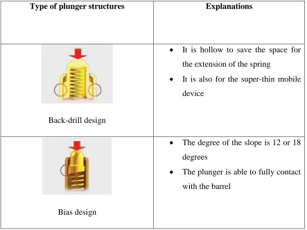
[image:13.612.116.566.372.567.2]6 2.1.1 Type of plunger structures of pogo pin
[image:14.612.107.550.352.683.2]There are two types of plunger structures which are Back-Drill Design and the Bias Design. For the tiniest pogo pin connector, back- drill design is the best selection. This is because the length of the spring on the back- drill design is longer than the depth of the barrel and when the force is applied it can reach the part which is the customer wants. The second type of plunger structure is biased design which is it can bring the low interconnection resistance where the interconnection between the pogo pin and an area of the IC package production is decreasing. Since making the plunger is able to contact with the edge of the barrel with 100%, therefore the end of the plunger is sliced like a bias style. Then it is also controlled the absolute of the consistency of the external contact- resistance.
Table 1: Type of plunger structures (Davis, L. (2012)
Type of plunger structures Explanations
Back-drill design
It is hollow to save the space for
the extension of the spring
It is also for the super-thin mobile
device
Bias design
The degree of the slope is 12 or 18
degrees
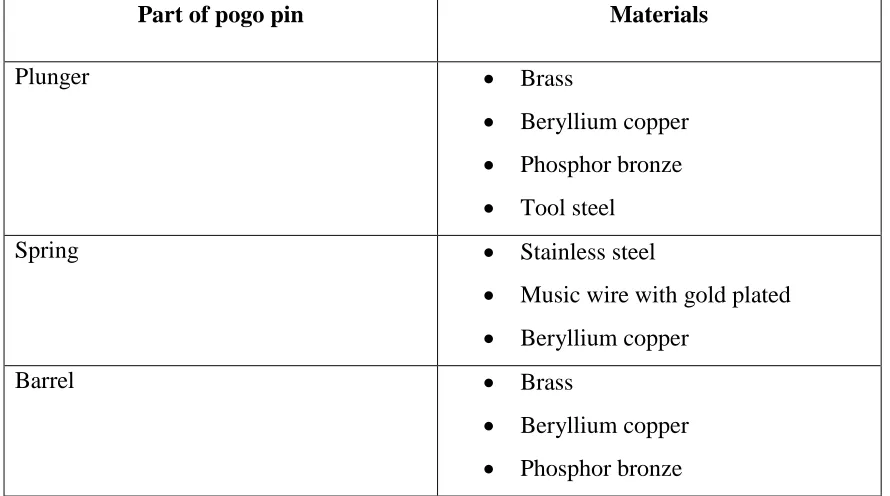
7 2.1.2 Type of material used of each part
[image:15.612.106.551.188.436.2]Table 2 shows about the material used for each part of pogo pin. This shows that each of the part is made up from different type of materials.
Table 2: Type of material in each part of pogo pin
Part of pogo pin Materials
Plunger Brass
Beryllium copper Phosphor bronze Tool steel
Spring Stainless steel
Music wire with gold plated Beryllium copper
Barrel Brass
Beryllium copper Phosphor bronze
2.2 Integrated Circuit (IC) Package
2.2.1 Definitions of the IC Package
8 2.2.2 Type of IC Package
There are some of the type of IC package which are through-hole, surface mount, chip carrier, pin grid arrays, flat packages, small outline packages, chip-scale packages, ball grid array, transistor and small pin count IC packages, and last but not least multi-chip packages. Each of it has difference functions and difference materials that are used in.
2.2.3 Package Type and Its Classification
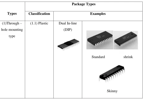
[image:16.612.111.572.340.661.2]2.2.3.1 Through- Hole Mounting Type
Table 3: Type of Through-Hole Mounting (Davis, L. (2012)
Types
Package Types
Classification Examples
(1)Through – hole mounting
type
(1.1) Plastic Dual In-line (DIP)
Standard shrink
9
Zigzag in-line
(ZIP)
Ceramic Standard DIP
Glass sealed ceramic DIP(CER-DIP)
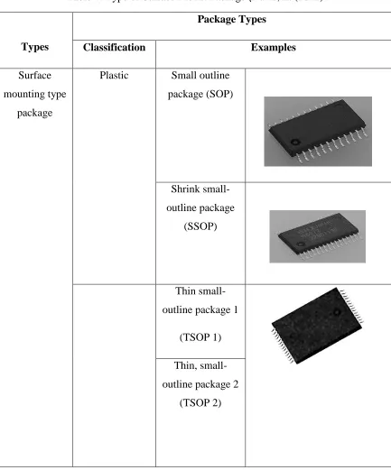
10 2.2.3.2 Surface Mount Type Package
Table 4: Type of Surface Mount Package (Davis, L. (2012)
Types
Package Types
Classification Examples
Surface mounting type
package
Plastic Small outline package (SOP)
Shrink small-outline package
(SSOP)
Thin small-outline package 1
(TSOP 1)
Thin, small-outline package 2
11
Quad flat package (QFP)
High heat dissipation QFP
Thin quad flat pack (TQFP)
Low-profile quad flat pack (LQFP)
12
Quad flat J-leaded (plastic
leaded chip carrier)
QFJ(PLCC)
Ball grid array/fine pitch
ball grid array
13 2.2.4 IC package category
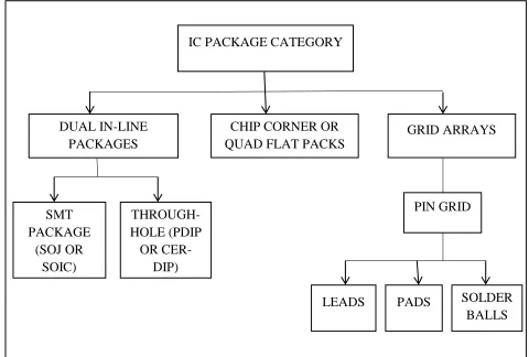
The IC package category is categorized in three categorized which are dual in-line package, chip corners, and also grid arrays. The dual in-line package is a package with the two rows of leads on the two sides of the package. There are two types of dual in-line package which are through-hole (PDIP OR CERDIP) and another one is an SMT package (SOJ OR SOIC) which is the surface mount technology. While for the chip corners are called as quad flat packs is a square package with leads on all four sides. Lastly the grid array which has the pins that are arranged in the grid and the pin grid consists of three parts which are the leads, pads and also solder balls.
[image:21.612.103.583.318.642.2]
Figure 3: IC package category
GRID ARRAYS CHIP CORNER OR
QUAD FLAT PACKS IC PACKAGE CATEGORY
DUAL IN-LINE PACKAGES THROUGH-HOLE (PDIP OR CER-DIP) SMT PACKAGE (SOJ OR SOIC)
14
Table 4: Category of IC packages (Davis, L. (2012) Category Of IC Packages Descriptions
Dual in-line package (DIP)
First generation IC package type Is a thru-hole device with the
lead with the space of 0.100 “ Mostly translate to the SOIC
packages for higher density applications
The body shape is rectangular
Quad flat pack (QFP)
High density
The body shape is square and rectangular
The size of the body is about
from 7mm to 40mm
Grid array Second generation of the IC package type
Thru-hole also but the size of
packages is reduced since the pin is moved to the underside of the package in a grid pattern
15
Small outline
J-Leaded(SOJ)
The lead pitch is decreased to 50
mil
Lead looks like the ‘j’ letter
which sometimes called J-leaded The body shape is rectangular
Small outline IC(SOIC)
First surface mount package Also called as the Gull Wing Mostly popular in the memory
16
2.3 Applications on the IC Package
2.3.1 Type of pogo pin
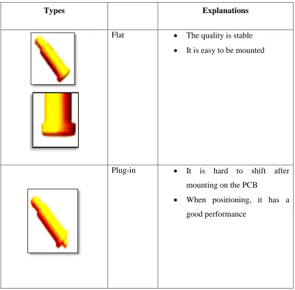
[image:24.612.107.538.256.679.2]Table 5 below shows the type of the pogo pin. There are some type of the pogo pin which are flat type, plug-in type, right-angle type, multiple types, bending type, double-ended pin and special spec type.
Table 5: Type of pogo pin (Davis, L. (2012)
Types Explanations
Flat The quality is stable It is easy to be mounted
Plug-in It is hard to shift after mounting on the PCB
When positioning, it has a