This is a repository copy of
Graphene electrodes for adaptive liquid crystal contact lenses
.
White Rose Research Online URL for this paper:
http://eprints.whiterose.ac.uk/98409/
Version: Accepted Version
Article:
Kaur, S, Kim, YJ, Milton, H et al. (8 more authors) (2016) Graphene electrodes for adaptive
liquid crystal contact lenses. Optics Express, 24 (8). 260968. pp. 8782-8787. ISSN
1094-4087
https://doi.org/10.1364/OE.24.008782
eprints@whiterose.ac.uk https://eprints.whiterose.ac.uk/
Reuse
Unless indicated otherwise, fulltext items are protected by copyright with all rights reserved. The copyright exception in section 29 of the Copyright, Designs and Patents Act 1988 allows the making of a single copy solely for the purpose of non-commercial research or private study within the limits of fair dealing. The publisher or other rights-holder may allow further reproduction and re-use of this version - refer to the White Rose Research Online record for this item. Where records identify the publisher as the copyright holder, users can verify any specific terms of use on the publisher’s website.
Takedown
If you consider content in White Rose Research Online to be in breach of UK law, please notify us by
Graphene electrodes for adaptive liquid crystal
contact lenses
S. Kaur,1,2,* Y.-J. Kim,1 H. Milton,1,3 D. Mistry,1,2 I. M. Syed,4 J. Bailey,1,2 K. S. Novoselov,1 J. C. Jones,1,2 P. B. Morgan,5 J. Clamp,6 and H. F. Gleeson1,2
1School of Physics and Astronomy, University of Manchester, M13 9PL, United Kingdom 2Present address: School of Physics and Astronomy, University of Leeds, Leeds, LS2 9JT, United Kingdom 3Present address: e-Vision Smart Optics, Inc., 1144 Tallevast, Suite 115, Sarasota FL 34243, United States
4
Department of Physics, University of Dhaka, Dhaka, 1000, Bangladesh
5Eurolens Research, University of Manchester, Manchester, M13 9PL, UK 6Ultravision CLPL, Leighton Buzzard, LU7 4RW, UK
*s.b.kaur@leeds.ac.uk
Abstract: The superlatives of graphene cover a whole range of properties: electrical, chemical, mechanical, thermal and others. These special properties earn graphene a place in current or future applications. Here we demonstrate one such application – adaptive contact lenses based on liquid crystals, where simultaneously the high electrical conductivity, transparency, flexibility and elasticity of graphene are being utilised. In our devices graphene is used as a transparent conductive coating on curved PMMA substrates. The adaptive lenses provide a +0.7 D change in optical power with an applied voltage of 7.1 Vrms - perfect to correct presbyopia, the
age-related condition that limits the near focus ability of the eye.
©2016 Optical Society of America
OCIS codes: (000.0000) General; (000.2700) General science.
References and links
1. P. Blake, P. D. Brimicombe, R. R. Nair, T. J. Booth, D. Jiang, F. Schedin, L. A. Ponomarenko, S. V. Morozov, H. F. Gleeson, E. W. Hill, A. K. Geim, and K. S. Novoselov, "Graphene-Based Liquid Crystal Device," Nano Lett. 8, 1704-1708 (2008).
2. K. S. Novoselov, A. K. Geim, S. V. Morozov, D. Jiang, Y. Zhang, S. V. Dubonos, I. V. Grigorieva , and A. A. Firsov, "Electric Field Effect in Atomically thin Carbon Films," Science 306, 666-669 (2004).
3. A. K. Geim, and K. S. Novoselov, "The rise of graphene," Nature Mater. 6, 183-191 (2007).
4. C. Lee, X. Wei, J. W. Kysar, and J. Hone, "Measurement of the Elastic Properties and Intrinsic Strength of Monolayer Graphene.," Science 321, 385-388 (2008).
5. A. A. Balandin, S. Ghosh, W. Bao, I. Calizo, D. Teweldebrhan, F. Miao, and C. N. Lau, "Superior Thermal Conductivity of Single-Layer Graphene," Nano Lett. 8, 902-907 (2008).
6. S. Bae, H. Kim, Y. Lee, X. Xu, J.-S. Park, Y. Zheng, J. Balakrishnan, T. Lei, H. R. Kim, Y. I. Song, Y.-J. Kim, K. S. Kim, B. Özyilmaz, J.-H. Ahn, B. H. Hong, and S. Iijima, "Roll-to-roll production of 30-inch graphene films for transparent electrodes," Nature Nanotech. 5, 574-578 (2010).
7. K. Chung, C. H. Lee, and G. C. Yi, "Transferable GaN Layers Grown on ZnO-Coated Graphene Layers for Optoelectronic Devices," Science 330, 655-657 (2010).
8. T. H. Han, Y. Lee, M. R. Choi, S. H. Woo, S. H. Bae, B. H. Hong, J. H. Ahn, and T. W. Lee, "Extremely efficient flexible organic light-emitting diodes with modified graphene anode," Nature Photonics 6, 105-110 (2012).
9. W. S. Koh, C. H. Gan, W. K. Phua, Y. A. Akimov, and P. Bai, "The Potential of Graphene as an ITO Replacement in Organic Solar Cells: An Optical Perspective," IEEE Journal of Selected topics in quantum electronics 20, 4000107 (2014).
10. X. Wang, L. Zhi, and K. Müllen, "Transparent, Conductive Graphene Electrodes for Dye-Sensitized Solar Cells," Nano Lett. 8, 323-327 (2008).
12. D. Kuzum, H. Takano, E. Shim, J. C. Reed, H. Juul, A. G. Richardson, J. de Vries, H. Bink, M. A. Dichter, T. H. Lucas, D. A. Coulter, E. Cubukcu, and B. Litt, "Transparent and flexible low noise graphene electrodes for simultaneous electrophysiology and neuroimaging," Nature Commun. 5, 5259 (2014).
13. D. W. Park, A. A. Schendel, S. Mikael, S. K. Brodnick, T. J. Richner, J. P. Ness, M. R. Hayat, F. Atry, S. T. Frye, R. Pashaie, S. Thongpang, Z. Ma, and J. C. Williams, "Graphene-based carbon-layered electrode array technology for neural imaging and optogenetic applications," Nature Commun. 5, 5258 (2014).
14. Fei Hui, Pujashree Vajha, Yuanyuan Shi, Yanfeng Ji, Huiling Duan, Andrea Padovani, Luca Larcher, Xiao Rong Li, Jing Juan Xu, and M. Lanza, "Moving graphene devices from lab to market: advanced graphene-coated nanoprobes," Nanoscale (2016).
15. H. E. Milton, H. F. Gleeson, P. B. Morgan, J. W. Goodby, S. Cowling, and J. H. Clamp, "Switchable liquid crystal contact lenses: dynamic vision for the ageing eye," Proceedings of SPIE 9004, 900401-900406 (2014). 16. H. E. Milton, P. B. Morgan, J. H. Clamp, and H. F. Gleeson, "Electronic liquid crystal contact lenses for the
correction of presbyopia," Opt. Exp. 22, 8035-8040 (2014 ).
17. H. E. Milton, P. D. Brimicombe, P. B. Morgan, H. F. Gleeson, and J. H. Clamp, "Optimization of refractive liquid crystal lenses using an efficient multigrid simulation," Opt. Exp. 20 11159-11165 (2012).
18. I. M. Syed, S. Kaur, H. E. Milton, D. Mistry, J. Bailey, P. B. Morgan, J. C. Jones, and H. F. Gleeson, "Novel switching mode in a vertically aligned liquid crystal contact lens," Optics express 23, 9911-9916 (2015). 19. A. R. Lingley, M. Ali, Y. Liao, R. Mirjalili, M. Klonner, M. Sopanen, S. Suihkonen, T. Shen, B. P. Otis, H.
Lipsanen, and B. A. Parviz, "A single-pixel wireless contact lens display," J. Micromech. Microeng. 21, 125014 (2011).
20. Y.-T. Liao, H. Yao, A. R. Lingley, B. A. Parviz, and B. P. Otis, "A 3-microW CMOS Glucose Sensor for Wireless Contact-Lens Tear Glucose Monitoring," IEEE J. Solid-state circuits 47, 335 (2012).
21. H. Langley, "Google's smart contact lenses just went from concept to reality," in
http://www.techradar.com/news/wearables/google-s-smart-contact-lenses-just-went-from-concept-to-reality-1302370(Techradar 2015).
22. W. N. Charman, "Restoring accommodation: a dream or an approaching reality?," Ophthalmic and Physiological Optics 25, 1-6 (2005).
23. C. Peng, Z. Jia, D. Bianculli, T. Li, and J. Lou, "In situ electro-mechanical experiments and mechanics modeling of tensile cracking in indium tin oxide thin films on polyimide substrates," J. Appl. Phys. 109, 1035301-1035307 (2011).
24. D. W. Berreman, "Optics in Stratified and Anisotropic Media: 4×4-Matrix Formulation," J. Opt. Soc. Am. 62, 502-510 (1972).
25. H. G. Yoon, N. W. Roberts, and H. F. Gleeson, "An experimental investigation of discrete changes in pitch in a thin, planar chiral nematic device," Liq. Cryst. 33, 503-510 (2006).
26. "emPower!™, the first electronic focusing prescription eyewear!," (2015), http://www.heitzoptical.com/Content/eyeglasses/lenses/pixeloptics/empower.aspx.
27. M. Hofmann, Y.-P. Hsieh, A. L. Hsu, and J. Kong, "Scalable, flexible and high resolution patterning of CVD graphene," Nanoscale 6, 289-292 (2014).
1. Introduction
The potential of graphene as transparent electrodes in liquid crystal (LC) devices was first demonstrated in 2008 by Blake et al. [1]. The device exhibited uniform switching and high optical transparency, stringent requirements for display applications, demonstrated for a single pixel of dimensions ~10µm in a conventional geometry with parallel glass substrates. The real advantages of graphene electrodes are apparent in non-conventional geometries, for applications where flexibility and transparency are key requirements and with much larger electrode areas. Graphene, being only one atom thick [2], and having a number of unique electrical [3], mechanical [4] and thermal [5] properties is fully compatible with flexible, curved LC devices. Furthermore, large roll to roll production of graphene [6] makes graphene a realistic candidate to be used in mass-produced flexible optoelectronic devices [7, 8], organic and solid state solar cells [9, 10], supercapacitors [11], neural imaging and opto-genetic applications [12, 13]. Recent advances in fabricating simple and low-cost graphene coated nanoprobes demonstrate the extensive potential graphene exhibits to be used in various applications and progressing its move from lab to market [14].
demonstrate th contact lens co
Electrically sw exciting addit 21]. The unde correct presby major concern in comparison adaptive cont refractive inde objects, there Unfortunately compatible wi as they quickl
2. Design and
The switchab substrates wit properties of geometric len
Fig. 1. (a) A sche PMMA substrate details (not to sca substrates provid lens is 7.8mm, m centre of the lens curved section of from the clarity demonstrates the flat substrate usin
The graphene chemical vapo and transfer p contact lens, PMMA and PMMA/graph of the remai transferred on film covered w used for exce contact lenses lathing or, m manufacture i
hat the transpa onstruction, m
witchable LC c tion to the ‘sma
erlying concep yopia, a condit ns in modern o n with other t tact lenses, an ex of the lens, eby replicating y, the transpare ith the highly c ly lose electrica
d construction
ble contact len th a lens-shape the LC conta s design, toget
ematic diagram of ‘A’ and Indium T ale) with the LC d de positive optical atching the curvat s is 50 µm. (b) is f the lens (6 x 6 m
of the text throu optical power of ng the same proces
e layer used in our deposition
process are de the graphene the graphene hene membrane
ining PMMA/ nto the PMMA
with a thin laye ellent intercon s (Fig. 1b). C more commonl is not only exp
arent, conducti aking it an obv
contact lenses w art contact lens pt here is to pr tion that affec optometry. Ada
treatments suc n electrical sig changing the l g the accomm ent conductive curved and flex al conductivity
n of the lens us
ns is made fro ed gap contain act lens and i her with the ch
the LC contact len Tin Oxide (ITO) o director parallel to
powers of +6.4±0 ture of the human c a photograph of mm2) so that whole
ugh the graphene-the lens substrate ss as used for depo
the constructi (CVD) growth escribed elsew film formed o on the other e was then rele /graphene laye A lens substrat
er (~100 nm) o nnects in wear Contact lenses y, injection m pensive, but th
a
ive and flexible vious choice of
were demonstr ses’ being prop rovide an elec ts all adults ov aptive contact ch as reading nal provides a lens power and modation mech coatings tradit xible substrate y.
sing graphene
om mating tw ning a LC, as its variable op hoice of LC an
ns constructed wit on the concave side
the lens substrate 0.1 D and +7.6±0. cornea. The thickn a contact lens sub curved area is act -coated substrate e. The average opt ositing it on the cur
ion of the LC h technique. Th where [6]. To
on one side of r side was re eased by disso ers, the whol tes. This proce of PMMA, with
rable and flex are usually fa moulding. Spu he curved plas
a
e nature of gra f electrodes for
rated recently [ posed by sever ctrically contro ver the age of lenses provide or multifocal a continuous c d allowing the hanism of the
tionally used in es required for
e electrode
wo polymethyl shown in Fig ptical power nd switching m
th a graphene elect e of substrate ‘B’. es (no voltage app .1 D respectively; ness of the LC laye bstrate with graph tive. (c) Demonstr lens. The text se tical transmittance urved substrates wa
contact lens w he details of th transfer the g f copper (Cu) emoved using olving the Cu.
le PMMA/gra ess results in a
h sheet resistan xible electroni abricated as si uttering of ITO
stic surfaces le
b
aphene can sim r such applicati
[15-18] and rep ral research gr ollable focus w f fifty and is o
e significant ad spectacles [22 change in the user to focus o younger eye in LC devices adaptive conta
lmethacrylate . 1. The overa are determine ode [15-18].
trode on the conve . The insert shows
lied). The convex ; the radius of cur
er between the sub hene deposited ont rates the excellent een in focus thro e of graphene dep as found to be 98%
was synthesize he graphene pr graphene film
foil was cove g oxygen plas After repeated aphene membr a high quality nce <1 kΩ/ th ic applications ingle units, wh O at the poin ead to issues a
c
mplify the ions. present an roups [19-which can one of the dvantages 2]. In the effective on nearby e [15-18]. are rarely act lenses, (PMMA) all optical ed by theex side of the s construction and concave rvature of the bstrates at the to the central transparency ugh the lens osited onto a % [1].
ed using a reparation onto the ered with sma. The d cleaning rane was graphene hat can be s such as
[image:4.612.151.462.320.412.2]with poor adhesion of ITO onto the substrates, uniformity and yield. In addition, ITO thin films are brittle [23], and therefore unsuitable for flexible applications. The production of graphene on the PMMA substrate and subsequent transfer onto the flexible, curved lens components, offers a clear route to mass production of the adaptive contact lenses.
Here, we used a commercially available nematic LC material (MLC-6648, Merck) exhibiting a positive dielectric anisotropy with a birefringence ∆n=0.07 and relatively a low viscosity, offering the potential for sub-second response time, ideal for a switchable focus contact lens. The LC ordinary refractive index, no, is similar to that of the PMMA substrates (1.49 at 633
nm), minimising Fresnel losses.
A key requirement of a LC device is uniform, controlled orientation of the director. In most devices an alignment layer is deposited on both electrodes and rubbed to provide a unique orientation direction. We found that no alignment layer is needed on the graphene substrate as both PMMA and graphene give good planar alignment. The overall preferred orientation in the contact lens is defined by the rubbing direction on the concave substrate, an approach similar to that used in the graphene-based pixel demonstrated by Blake et al. [1]. The use of the rubbed polyimide alignment layer necessitated the ITO electrode. We note that for this planar lens geometry, the ‘off’ state focus is polarization dependent. This feature, as well as methods of overcoming such a dependence are discussed in detail in [15-18].
3. Investigation of lens quality and operation
Several measurements were made to investigate the quality and operation of the lens. Dielectric spectroscopy was used to determine the threshold voltage, Vth for switching the
lens. On application of a voltage just above Vth, the LC director begins to orient parallel to the
electric field and the measured device capacitance increases, reaching a maximum at voltage far above the threshold. The Vth of the contact lens device was found to be +2.1±0.2 Vrms from
voltage-dependent capacitance measurements.This agrees well with the value calculated using the expression for a parallel device: Vth= (k11/ o )1/2, where o is the permittivity of free
space and k11 and are the splay elastic constant and dielectric anisotropy of the liquid
crystalline material respectively. The values for k11 and were measured to be 11.0±1.0 pN
[image:5.612.136.483.453.506.2]and 2.9±0.2 respectively in a separate experiment using a planar aligned LC contained between two parallel glass plates, leading to a calculated value of Vth= 2.1±0.2 Vrms.
Fig. 2. Textural micrograph images (maximum transmission, i.e. rubbing direction at 45û to the crossed polarizers) of the LC contact lens at room temperature as the applied voltage is varied. The change in the birefringence colours can clearly be observed as the voltage increases from (a) 0 Vrms to higher voltages (b-e). The images have been taken near
the centre of the lens; the faint concentric lines are sub-micron inhomogeneities in the PMMA surfaces caused by circular lathing during manufacture. The scale for all images is as marked on the lower right hand side of Fig. (a).
Polarizing microscopy was used to observe the texture and hence evaluate the quality of the LC alignment in the lenses. The uniform birefringence colours seen in Fig. 2 indicate both excellent planar alignment of the director and uniformity of construction. Fig. 2a shows the textural micrograph while no voltage was applied to the contact lens. Figs. 2b-e clearly show the change in birefringence colours when voltages higher than the threshold (2.1 Vrms) were
applied. The changing colours with the increasing voltage are associated with the change in the effective birefringence which is in turn due to an effective change in the extraordinary refractive index (ne) with increasing voltage. These indices were determined in a conventional
device from fitting the reflection spectra using the Berreman methodology [24] with further
details in Ref 1.48, which ap results in a b power require single alignme
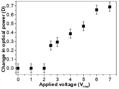
Fig. 3. The volta optical power is o
The focal pow previously [15 contact lens a contact lens in Vth of the con
Vrms, which a
micrographs ( the continuou region correct as viewing co with that calc results in the m
Fig. 4(a) The PSF (b) The MTF cur exhibit MTF50 v lens with and wit small optical chan
The optical q function (PSF beam profiler used to correc on the optical spatial freque values (spatia MTF curves. respectively. F combined res applied are 0.
0 Vr
f. [25]. On app pproaches no, m
birefringence c ed for an adapt ent layer produ
age-dependence of observed and Vth is
wer of the len 5]. Briefly, an and the point of
ncreases with ntact lens deduc again agrees w (Fig. 2). The c us change in op tion which is im omputer screen culated using t
maximum opti
F measurements o ves of the LC con values of 0.52 and thout the applicati nge of +0.70.1 D.
quality of the c F) and the mod placed at the p ct aberrations i l rail. The MT encies and was al frequency at Fig. 4a shows Fig. 4b compa olving power .52 and 0.63 lp
ms 7.1 V
lication of a h measured sepa hange of 0.06 tive contact len uces a lens with
f the change in op s consistent with c
ns was measu n expanded 10m
f focus was fou applied voltag ced from the op with the capac correction to p ptical power of mportant as it ns. The measu he thick lens e cal power chan
of the LC contact l ntact lens compared 0.63 line pairs/mr ion of 7.1 Vrms. T
contact lens w dulation transf point of focus induced throug TF of the lens s generated by t 50% modulat the PSFs of th ares MTF curv
of the substrat p/mrad respect 0 1 0.0 0.1 0.2 0.3 0.4 0.5 0.6 0.7 C h a n g e i n o p ti c a l p o w e r (D ) 0 0.0 0.2 0.4 0.6 0.8 1.0 N o rm a li s e d c o n tr a s t Vrms (a)
igh voltage, ne
arately as 1.47. 6, successfully ns. The microg h excellent opt
ptical power of the capacitance measur
ured as a func mW 632.8 nm und using a be ge (7.1 Vrms) c
ptical power m citive response resbyopes requ ffered by this s
would allow v ured change in equation. Mor nge (+0.7±0.1
lens at 0 and 7.1 V d with that of the rad respectively. (c The relatively sma
was measured fer function (M
of the expande gh the clampin quantifies its y taking the Fo
tion) are used he contact lens ves of the conta
tes ‘A’ and ‘B tively demonst
2 3 4 5
Applied voltage (Vrms)
1 2 3
Multiplied MTF of s Constructed lens (0 Constructed lens (7
Spatial frequency (cycles/mra
e changes from
Therefore, the demonstrating graph images d
tical quality.
e adaptive contact urements and the op
ction of applie m laser beam w
eam profiler. T hanging by +0 measurements w
e (Vth=2.1±0.2
uires an additi system offers t vision correctio n optical powe reover, an appl
D).
Vrms respectively a
substrates. The OF c) Images of text b all change observe
quantitatively MTF). The PSF
ed laser beam. ng of the conta
ability to reso ourier transfor for a quantita s at applied vo
act lens at diff B’. MTF50 va
trating similar
6 7
4 substrates 0 Vrms)
7 Vrms)
adians)
(b)
m 1.54 to a min e application o g the change i demonstrate tha
t lens. A continuo ptical micrographs
ed voltage as was passed thr The optical pow
0.7±0.1 D (Fig was found to b 2 Vrms) and th
ional optical p the possibility on for applicat er is in good a lied voltage of
at the appropriate FF and ON states brought into focus ed in the two imag
using the poi F was capture Additional len act lens when olve details of rm of the PSF ative comparis ltages of 0 and ferent voltages alues for 0 and r optical qualit
nimum of f 7.1 Vrms
in optical at using a
ous change in s.
described rough the wer of the g. 3). The be 2.0±0.5 he optical power and of a mid-tions such agreement f 7.1 Vrms
focal planes. of the device s with the LC ges due to the
int spread d using a nses were mounting f different F. MTF50 on of the d 7.1 Vrms
s with the d 7.1 Vrms
[image:6.612.118.486.407.487.2]states. The calculated MTF50 for the combined substrate system is 1.1 lp/mrad. We can conclude that though the system is limited by the substrates, the OFF and ON state of the LC lens are comparable making it an excellent first demonstration of a graphene electrode based lens that can correct presbyopia. The optical quality of the contact lens at 0 and 7.1 Vrms is
qualitatively demonstrated in Fig. 4c by using a DSLR camera. A change in magnification of the text demonstrates the +0.7±0.1 D increase in optical power of the contact lens.
An important parameter for the LC contact lens is the electro-optic response time. This was measured by placing the contact lens on a polarizing microscope and monitoring the change in intensity of monochromatic (632nm) light with a photodiode as the lens was switched ‘on’. At 5 Vrms the response time, ON, was 0.6±0.2 seconds. The response time of a parallel device is
given by , where is the LC viscosity and d the device
thickness. ON was measured to be 3.5±0.4ms for a 5µm thick parallel device, so a 60µm thick
device should have ON=0.5±0.1 seconds, is in good agreement with the contact lens response
using an average LC layer thickness of 60µm. This measured ON is comparable to the blink of
an eye (a few hundred milliseconds) which is sufficiently fast for this application; indeed, Pixel Optics marketed LC spectacles with the phrase ‘focus as fast as you can blink your eye’ [26]. The ‘off’ time for a parallel device is and we note that our design can improve both the on and off times by reducing the LC layer thickness; a factor of 10 decrease in response time is achieved by reducing the average lens thickness by a factor of ~3.
4. Conclusions
An adaptive LC contact lens with a graphene electrode has been successfully developed with an active area that covers the whole of the curved lens. The optical transparency, flexibility, low resistivity, good adhesion and stability of graphene make it an ideal candidate for use in contact lenses to correct presbyopia. The graphene adhered well to the PMMA substrate and the transmittance through the graphene electrode on the contact lens substrate is comparable to that of ITO. Importantly the flexibility of graphene makes the manufacture of these single contact lens units much easier. Using graphene for the electrodes avoids problems associated with using ITO, namely the requirement of a hard coat layer, expensive sputtering of ITO and low yields.
The lens developed is capable of providing a continuous change in optical power change of up to 0.7±0.1 D, switching the optical compensation continuously between far and near vision. The lens exhibited excellent alignment and optical quality with the use of a single alignment layer. The response time of the device was much less than a second and simple measures such as reducing the LC layer thickness or increasing the driving voltage will achieve response times better than 1/20th second, a typical response time for the human eye.
The potential for graphene electrodes in contact lenses is not just a consequence of the excellent optical and electro-optical performance; using graphene electrodes opens up new possibilities for the manufacture of flexible contact lenses. The flexibility of graphene would be advantageous if applied to soft lenses (hydrogels) which are commonly used contact lens materials. Moreover, the layer of PMMA on the top of graphene would help to inhibit entry of moisture, ions or gases in the lens containing LC. Patterning with graphene is already possible [27] and if applied to the lenses, will make the contact lens assembly much simpler. Our current aim is working towards a self-contained wirelessly operated device which will revolutionise the contact lens industry.
All of the source data for this paper can be found in DOI: http://doi.org/10.5518/27
Acknowledgements