UNIVERSITI TEKNIKAL MALAYSIA MELAKA
WIRELESS PHONE CHARGER
BY USING
INDUCTIVE CHARGING
This report submitted in accordance with requirement of the Universiti Teknikal Malaysia Melaka (UTeM) for the Bachelor Degree of Electronic Engineering
Technology (Industrial Electronic) with Honours.
by
AMRU SHAHRIL BIN ISHAK B071310928
921118-14-5229
I
DECLARATION
I hereby, declared this report entitled “Wireless Phone Charger by using Inductive Charging” is the result of my own research except as cited in references
Signature : ………
Author’s Name : ………
II
APPROVAL
This report is submitted to the Faculty of Engineering Technology of Universiti Teknikal Malaysia Melaka as a partial fulfilment of the requirement for the degree of Bachelor of Electronic Engineering Technology (Industrial Electronic) with Honours. The member of the supervisory committee is as follow.
III
ACKNOWLEDGEMENT
Bismillahirrahmaanirrahim,
In the name of Allah S.W.T, the most compassionate and the most merciful.
Firstly, thanks to Allah S.W.T because giving me a good health and endurance to do this final year project.
Secondly, I would like to deeply express my gratitude and appreciation to my supervisor, Madam Izadora binti Mustaffa for her guidance, support, encouragement and helping to finish my final year project.
IV
ABSTRACT
IV
ABSTRAK
Cas induktif ialah teknik yang menggunakan medan megnetik untuk pengalihan tenaga, seperti didalam projek ini, Voltan. Akan tetapi, tiada kajian terbuka mengenai keluaran lebih dari satu dengan menggunakan cas induktif. Projek ini cuba untuk mereka cipta sistem pengecas telefon pintar untuk keluaran banyak. Konsep keluaran lebih dari satu diramalkan sebagai jimat tenaga semasa cas lebih dari satu telefon pintar pada satu masa. Sejak projek ini ialah mengenai
VI
TABLE OF CONTENT
Acknowledgement III
Abstract IV
Abstrak V
Table of Content VI
List of Tables VIII
List of Figures IX
CHAPTER 1: INTRODUCTION
1.1 Introduction 1
1.2 Problem Statement 1
1.3 Objectives 2
1.4 Work Scope 2
1.5 Conclusion 2
CHAPTER 2: LITERATURE REVIEW 2.1 Introduction 3
2.2 Traditional Charging 3
2.2.1 Transformer 4
2.2.2 Rectifier 5
2.2.2.1 Half wave rectifier 5
VII
2.2.3 Voltage Regulator LM7805 7
2.2.4 USB Cable 7
2.2.5 Micro USB 9
2.3 Inductive Charging (Wireless charging) 10
2.3.1 Oscillator 11
2.3.1.1 RC Oscillator 11
2.3.1.2 LC Oscillator 12
2.3.2 Air Core Transformer 13
2.4 Conclusion 13
CHAPTER 3: METHODOLOGY 3.1 Introduction 14
3.2 Creating Coils 14
3.3 Vin effect on air core transformer coils 17
3.4 Resonant Frequency of air core transformer coils 17
3.5 Distance Between air core transformer coils 17
3.6 Offset between the air core transformer coils 17
3.7 Prototype Development 18
3.7.1 Capacitor 18
3.7.2 BJT 19
3.7.3 Regulator IC 20
3.7.4 Diode 21
3.7.5 Oscillator 22
3.7.6 Full bridge rectifier and 5VDC regulator 23
3.8 PCB Circuit Development 25
VII
CHAPTER 4: RESULT AND ANALYSIS
4.1 Introduction 29
4.2 Result of Vin effect on air core transformer coils 29
4.3 Result of Resonant Frequency of air core transformer coils 30
4.4 Result of Distance Between air core transformer coils 31
4.5 Result of Offset between the air core transformer coils 32
4.6 Result of coupling factor between the air core transformer coils 33
4.7 Result of offset between primary and secondary circuits 36
4.8 Result of distance between primary and secondary circuit 37
4.9 Multiple phone charging capabilities 37
4.10 Conclusion 38
CHAPTER 5: CONCLUSION 5.1 Conclusion 39
5.2 Future recommendation 39
VIII
LIST OF TABLES
3.1 Vin that will be tested on coils 17
3.2 Frequency tested 18
3.3 Distance tested 18
3.4 Offset distance tested 19
3.5 Features of IC 7805 22
3.6 Description of Pin Terminal 22
4.1 Vin effect on Vout 31
4.2 Frequency effect on Vout 32
4.3 Distance effect on Vout 33
4.4 Offset effect on Vout 34
4.5 Frequency effect on Vout and k (coupling co-efficient) 35
4.6 Distance effect on coupling co-efficient 36
4.7 Offset effect on coupling co-efficient 37
4.8 Offset to charging phone for 1 output 38
LIST OF FIGURES
2.1 Block diagram of traditional charger 4
2.2 Half wave rectifier and activation on positive phase 5
2.3 Full wave rectifier and activation on positive and negative phase 6
2.4 USB wiring pin 7
2.5 USB wiring colour code 8
2.6 Mirco USB wiring pin 9
2.7 Block diagram of inductive charging 10
2.8 Basic RC oscillator circuit 12
2.9 Basic LC circuit 13
3.1 Coil making process 16
3.2 Completed coils 16
3.3 Illustration on How the Smoothing Capacitor Functioning 20
3.4 BJT 2N2222A pin configuration 21
3.5 LM 7805 22
3.6 1N5817 diode 23
3.7 Breadboard testing oscillator circuit 24
3.8 Colpitt’s oscillator on Proteus on primary circuit 24
3.9 Breadboard testing Full bridge rectifier and 5VDC regulator 25
3.10 Full bridge and rectifier on Proteus on secondary 26
3.11 ISIS Interface for primary 27
3.12 ISIS Interface for secondary 27
3.13 ARES Interface for primary 28
3.14 ARES Interface for secondary 28
3.15 Completed PCB board for primary 29
4.1 Graph Vin effect in Vout 32
4.2 Graph frequency effect on Vout 33
4.3 Graph distance effect on Vout 34
4.4 Graph Offset effect on Vout 35
4.5 Frequency on coupling co-efficient 36
4.6 Distance effect on coupling co-efficient 37
1
CHAPTER 1
INTRODUCTION
1.1 Introduction
Nowadays, the use of smart phone is increased by second. However there are several problems that might occur when using the smart phone. As the phone is used with batteries supply, during charging process, sometimes, the wires that connecting the phone with charger is prone to break. One of the solutions is to use wireless energy transfer to set movement of wire in a fixed place inside the phone. This will eliminate the breakage of copper inside the wire that connecting the phone with charger. Since the inductive charging use magnetic field to transfer energy, an idea come that to reduce, or improve energy saving during those charging phase. The idea and problem creates an opportunity to develop a working wireless phone charger using inductive charging with capabilities of multiple charging, hence the project is started.
1.2 Problem Statement
2
1.3 Objectives
The objectives of this project are:
1. To investigate the different design of phone charger.
2. To study the capabilities for multiple phone charging using inductive charging
3. To develop a wireless phone charger system.
1.4 Scope
The scopes of this project are to build prototype which is an inductive charging that can only charge a phone that using micro USB cable for charging, with 5VDC in.
In this project, Proteus Software will be used to design the circuit for the wireless phone charger using inductive charging system. From the design done, PCB layout will be processed for the prototype.
This project also use LC oscillator to create an oscillating circuit to induce the voltage to the coil of primary, as energy transfer method.
This project also cover until up to 2 devices for charging using prototype of wireless phone charger using inductive charging.
1.5 Conclusion
3
CHAPTER 2
LITERATURE REVIEW
2.1 Introduction
Cell phone chargers now days are being standardized mostly because of the power capabilities and wide availability of the USB connectors. Since USB delivers 5 V, all new cell phones are made to be compatible with this voltage level. However, one of the most frequent failures in chargers for rechargeable batteries of compact electronic devices, such as the cellular phone, is from the mechanical contact. Energy transfer utilizing inductive coupling can overcome this contact failure problem by eliminating requirement for mechanical contact from USB for charging. In a comparative study by S. Ho, J. Wang, W. Fu and M. Sun, it is found that a wireless energy transfer technology is feasible to recharge batteries, particularly in implant devices (Ho et al., 2011). By this case we can build in this charger, the primary core of the transformer is in the charger unit and the secondary is attached to the phone.
2.2 Traditional Charging
4
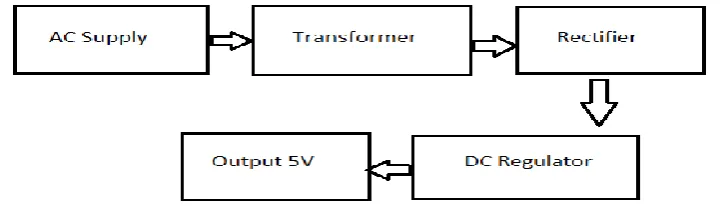
[image:16.595.145.506.130.233.2]damaged at connector phone wasted. Example of basic charging is shown in Figure 2.1 below.
Figure 2.1: Block diagram of traditional charger
2.2.1 Transformer
A transformer is an electrical device that capable to either step up (increase the AC voltage) or either step down (decrease the AC voltage). The capability of doing so is based on electromagnetic induction, which, the induction produces an emf (electromotive force) within a material that conducts electricity which is exposed to time varying magnetic fields. A different current in primary will create a magnetic flux in the transformer material that conduct electricity (core) and this will cause varies of magnetic field of secondary winding, which later will cause an induction of emf at secondary winding thus create a current flow, either high or lower than primary (Calvert, 2001). The secondary high or low output compared to the primary is based on number of turns, in primary and secondary, which can be interpreted as formula below
.
where V2 is voltage at secondary, V1 voltage at primary, I1 is current at
primary, I2 current at secondary, N1 number of turns (coiling) at primary,
and N2 is number of turns (coiling) at secondary. However, this is an ideal
5
transfomer have some losses due to eddy current, and/or heat produced by electricity at its core.
2.2.2 Rectifier
A rectifier is an electronic circuit that convert low AC voltage to a low DC voltage. The process of changing positive and negative cycle of voltage to a steady or positive only cycle of voltage is known as rectifying. A basic rectifier use a diode to block a voltage from going positive to negative cycle as diode capable of stopping voltage from flowing from one path to another. Since the capability of diode is to stop flow from one path to another, a single diode is enough to change AC voltage to DC voltage. Since the project only use single phase supply for common usage at home, the project will use either half wave rectifier or full wave rectifier. It is need to be reminded that usage of rectifier will produce a loss around 0.7 Volt per diode use in that particular wave direction.
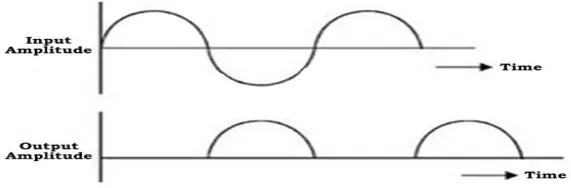
2.2.2.1 Half wave rectifier
[image:17.595.177.463.625.719.2]A half wave rectifier is a rectifier use only single diode to block the incoming AC from flowing back. However, there is limit in half wave rectifier, such as, since the diode only blocks half of the full wave of AC voltage; another half of the AC voltage is wasted. Since the wasted voltage, half wave rectifier only produce or yield half or lower voltage output. The half wave also produce more noise compared to full wave rectifier, thus more filtering to eliminate noise of AC, and produce better output (Knott, 1999). Example Figure 2 below shows a positive cycle of a basic half wave rectifier.
6
2.2.2.2 Full wave rectifier
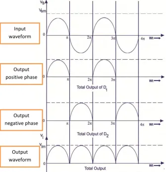
[image:18.595.125.461.198.545.2]A full wave rectifier uses both, negative and positive cycle of AC voltage thus, maximizing the output voltage, and creating lesser power loss. The design of full wave rectifier is shown in Figure 2.3 below
Figure 2.3: Full wave rectifier activation on positive and negative phase
Example shown in Figure 2.3 above, the full wave rectifier use all of voltage cycle. And since the voltage cycle is both forward biased, the output is a pulsating DC that is easier to smooth noises by using a capacitor. However, compared to half wave rectifier, for each cycle positive or negative of full wave rectifier, the output is using two diodes, thus need to be reminded that compared to half wave rectifier, the output of full wave rectifier have losses around 1.7 volt.
Input waveform
Output positive phase
Output negative phase
7
2.2.3 Voltage Regulator LM7805
A typical commonly used for 5 volt output voltage regulator is LM7805. It is capable to be used in normal condition temperature between -40°C and 125°C. Since smart phone use around 5 volt 1 amp input for charging, the LM7805 is suitable choice to regulate the output to desired value. The LM7805 also small enough to be fit in casing of typical smart phone. Since the voltage in capability of LM7805 maximum of 35 volt, it is easier to control the output of rectifier, and simpler circuit for creating a stable 5 volt 1 amp output circuit (fairchildsemi.com, 2014).
2.2.4 USB cable
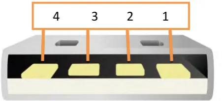
[image:19.595.217.443.528.631.2]Universal Serial Bus (USB) is a hardware interface for communicating devices such as keyboards, mouse, joystick, storage device, smart phone etc. According to USB 2.0 Specification Engineering Change Notice (ECN) #1: Mini-B connector (usb.org, 2000), the design for USMini-B 2.0 is shown in Figure 2.4 below
Figure 2.4: USB wiring pin
8
Figure 2.5: USB wiring colour code
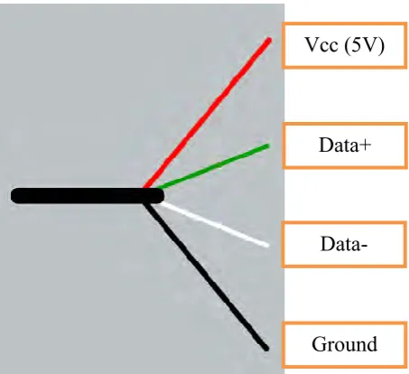
Requirement for using USB is to understand the colour coding. The Figure 2.4 and Figure 2.5 show the colour coding of a mass used USB A type connector. If you cut open a USB 2.0 cable you will see 5 different wires. There is a shielding wire which protects data transfer between devices from interferences. There is also, according the Figure 2 which have Red and Black wire where power is transferred from one device to another device. Then there are White and Green wires which form D- and D+ which are used for data transfer. The USB bus can supply 5VDC regulated power to each port on pins 1 and 4 according to Figure
2.44, the pins 1 and 4 are longer than the data pins to ensure that the power pins connect first and next the Data pins. Low power devices can then therefore be powered from USB there by eliminating the need of separate power supply such as power adapter.
Vcc (5V)
Data+
Data-
9
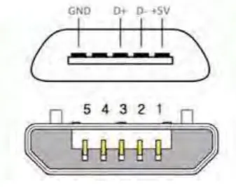
2.2.5 Micro USB
[image:21.595.242.411.300.434.2]As the phasing out of mini USB (Miller, 2007), the usage of micro USB is suggested as next generation charging and data transfer female and male connector port. Typical smart phone have a port that used for both charging and for data transfer. A layout of micro USB is shown in Figure 2.6 below, based on micro USB datasheet (micro-USB_1_01, 2011).
Figure 2.6: Mirco USB wiring pin
10
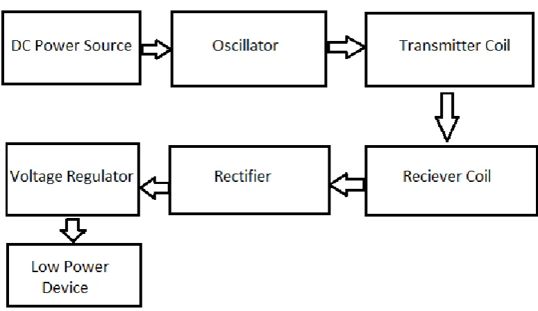
2.3 Inductive Charging (Wireless charging)
[image:22.595.129.517.254.478.2]Inductive charging is capable to charge wirelessly a device, whether how big or small the devices are. An example of current usage of inductive charging is to charge a hybrid or electric transport (Wu et al., 2011). A basic understanding of inductive charging is a transmission of power is based on coil where it is near each other. A block diagram in Figure 2.7 show a basic components in inductive charging
Figure 2.7: Block diagram of inductive charging
11
Recent improvements to this resonant system include using a movable transmission coil (i.e. mounted on an elevating platform or arm) and the use of other materials for the receiver coil made of silver plated copper or sometimes aluminium to minimize weight and decrease resistance due to the skin effect. However, the weakness of inductive charging will cause some losses during transfer of energy from primary to secondary coil.
2.3.1 Oscillator
Oscillator is an electronic circuit that produces an oscillating wave of either current of voltage. Typically, oscillator produces sine wave. Oscillator functioning by changing DC to AC. Since this project use inductive charging, a way to change DC to AC is required to oscillate through inductor for transmission through air medium.
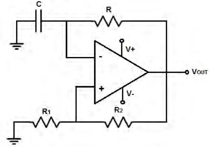
2.3.1.1 RC Oscillator
12
Figure 2.8: Basic RC oscillator circuit using op-amp
2.3.1.2 LC Oscillator