This is a repository copy of
Electrically pumped continuous-wave III–V quantum dot lasers
on silicon
.
White Rose Research Online URL for this paper:
http://eprints.whiterose.ac.uk/111812/
Version: Accepted Version
Article:
Chen, S., Li, W., Wu, J. et al. (9 more authors) (2016) Electrically pumped
continuous-wave III–V quantum dot lasers on silicon. Nature Photonics, 10. pp. 307-311.
ISSN 1749-4885
https://doi.org/10.1038/nphoton.2016.21
[email protected] https://eprints.whiterose.ac.uk/ Reuse
Unless indicated otherwise, fulltext items are protected by copyright with all rights reserved. The copyright exception in section 29 of the Copyright, Designs and Patents Act 1988 allows the making of a single copy solely for the purpose of non-commercial research or private study within the limits of fair dealing. The publisher or other rights-holder may allow further reproduction and re-use of this version - refer to the White Rose Research Online record for this item. Where records identify the publisher as the copyright holder, users can verify any specific terms of use on the publisher’s website.
Takedown
If you consider content in White Rose Research Online to be in breach of UK law, please notify us by
Electrically Pumped Long Lifetime Continuous-Wave III-V
Quantum-Dot Lasers Directly Grown on Silicon Substrates
Siming Chen1*, Wei Li2, Jiang Wu1, Qi Jiang1, Mingchu Tang1, Samuel Shutts3, Stella N. Elliott3, Angela Sobiesierski3, Alwyn J. Seeds1, Ian Ross2, Peter M. Smowton3, and Huiyun Liu1*
Reliable, efficient electrically pumped silicon-based lasers would enable full integration of photonic and electronic circuits, but have previously only been realized by wafer bonding. Here, we demonstrate the first continuous-wave InAs/GaAs quantum-dot lasers directly grown on silicon substrates with a low threshold current density of 62.5 A/cm2, a room-temperature output power exceeding 105 mW, lasing operation up to 120
o
C, and over 3,100 hours of continuous-wave operating data collected, giving an extrapolated mean time to failure of over 100,158 hours. The realization of high-performance quantum-dot lasers on silicon is due to the achievement of a low density of threading dislocations on the order of 105 cm-2 in the III-V epilayers by combining a nucleation layer and dislocation filter layers with in-situ thermal annealing. These results are a major advance towards silicon-based photonics and photonic-electronic integration, and could provide a route towards reliable and cost-effective monolithic integration of III-V devices on silicon.
Increased data throughput between silicon processors in modern information processing demands unprecedented bandwidth and low power consumption beyond the capability of conventional copper interconnects. To meet these requirements, silicon photonics has been under intensive study in recent years1,2. Despite rapid progress being made in silicon-based light modulation and detection technology and low-cost silicon optoelectronic integrated devices enabled by the mature CMOS technology3,4, an efficient reliable electrically pumped laser on a silicon substrate has remained an unrealized scientific challenge5. Group IV semiconductors widely used in integrated circuits, e.g. silicon and germanium, are inefficient light-emitting materials due to their indirect bandgap, introducing a major barrier to the development of silicon photonics. Integration of IIIÐV materials on a silicon platform has been one of the most promising techniques for generating coherent light on silicon. IIIÐV semiconductors with superior optical properties, acting as optical gain media, can be either bonded or epitaxially grown on silicon substrates6-11, with the latter approach being more attractive for large scale, low-cost, and streamlined fabrication. However, until now, material lattice mismatch and incompatible thermal expansion coefficients between IIIÐV materials and silicon substrates have fundamentally limited the monolithic growth of IIIÐV lasers on silicon substrates by introducing high-density threading dislocations (TDs)12.
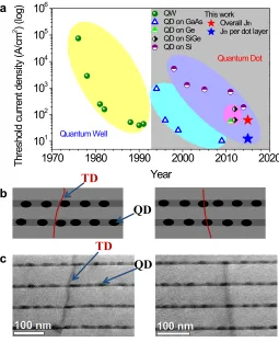
Lasers with active regions formed from III-V quantum dots (QDs), nano-size crystals, can not only offer low threshold current density (Jth) but also reduced temperature sensitivity
13-17
. As shown in Figure 1a, within less than 10 years, the performance of QD lasers has surpassed state-of-the-art quantum-well (QW) lasers developed over the last few decades in terms of Jth. QD lasers have now been demonstrated with nearly constant Jth, output power (Pout), and differential efficiency at operating temperatures of up to 100 ¡C18. Very recently, IIIÐV QD structures have drawn growing attention for the implementation of compound semiconductor lasers on silicon substrates8-10,19. This is because QDs have also been proved to be less sensitive to defects than conventional bulk materials and QW structures, due to carrier localization and hence a reduced interaction with the defects20. As shown in Figure 1b and c, a
1
threading dislocation can only ÒkillÓ a very limited number of QDs, leaving the rest intact and able to provide optical gain. The enhanced tolerance to defects by localized states has also been witnessed in defect-insensitive nitride semiconductors, which are now used for the most efficient lighting technology21. More importantly, Figure 1b and c also reveal that the threading dislocation can be either pinned or propelled away from QDs. Therefore, the strong strain field of a QD array also prevents the in-plane motion of dislocations, and therefore superior reliability is expected from QD lasers compared with QW or bulk devices, even in the presence of high-density dislocations22,23.
These unique properties of QDs provide a promising route towards monolithic III-V on silicon (III-V/Si) integration. As shown in Figure 1a, III-V QD lasers grown on silicon are rapidly approaching the performance of those grown on native GaAs substrates24,25. In addition, high-performance QD lasers have been successfully demonstrated on Ge-on-Si and Ge substrates, offering an albeit indirect route to III-V/Si integration9,10,26. However, it would be more attractive to realise a laser which did not require the intermediate germanium layer both because the requirement for the germanium layer restricts the range of silicon circuits to which it can be applied and since it is difficult to couple light through this layer to a silicon waveguide due to the high optical absorption coefficient of germanium at telecommunications wavelengths. Therefore, a high performance III-V laser directly grown on silicon is the preferred solution for silicon photonic-electronic integration.
Although QD lasers have demonstrated superior performance on silicon substrates in the last
few years, our previous publications8,24,25 indicate that epitaxially grown GaAs-on-Si
substrates are much inferior when compared to bulk GaAs substrates in terms of total defect
density, typically over 2×106 cm-2 compared with the order of 103-104 cm-2 for a GaAs
substrate27. Furthermore, a high-performance electrically pumped continuous-wave (c.w.) QD
laser directly grown on a silicon substrate has not yet been demonstrated. Here, by developing
high-quality GaAs films with low TD density in the range of 105 cm-2, we experimentally demonstrate high-performance 1310-nm InAs/GaAs QD lasers directly grown on silicon, with a record low Jth, high power, and high-temperature c.w. operation. Most significantly, a large number of operating hours with negligible degradation has been demonstrated for III-V lasers directly grown on silicon substrates for the first time.
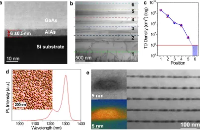
In this work, InAs/GaAs QD lasers were directly grown on silicon substrates using a solid-source molecular beam epitaxy (MBE) system. In order to realize high-quality IIIÐV lasers on silicon, it is necessary to minimize the impact of dislocations. Otherwise, TDs propagating into the active region will form nonradiative recombination centers and reduce minority-carrier lifetimes23, leading to degradation of laser performance. To realize practical monolithic QD lasers with the performance and reliability necessary for monolithic integration, several strategies have been developed and employed in the current work. First, in order to prevent the formation of antiphase domains (APDs) while growing polar III-V materials on non-polar silicon substrates, phosphorus-doped Si(100) wafers with 4¡ offcut to the [011] plane were used28 (FigureS1, Supplementary information I). A thin nucleation layer made of AlAs was deposited by migration enhanced epitaxy using alternating Al and As4 flux
at a low growth temperature of 350 ¡C. Figure 2a shows the high angle annular dark field scanning transmission electron microscopy (TEM) image of the interface. The thin AlAs nucleation layer has suppressed three-dimensional growth and provides a good interface for succeeding III-V material growth19. Following the AlAs nucleation layer, a three-step growth technique of GaAs epitaxial growth was performed8,29. The three layers of GaAs were grown at 350 ¡C, 450 ¡C, and 590 ¡C for 30 nm, 170 nm, and 800 nm, respectively. As shown in Figure 2b, most of the defects are well confined in the first 200 nm region thanks to the nucleation layer and multi-step temperature growth but still a high density (109 cm-2) of TDs are seen to propagate towards the active region. To further improve the material quality, strained layer superlattices (SLSs) were grown as dislocation filter layers (DFLs) on the top of the GaAs buffer layer. Each SLS is made of five periods of 10-nm In0.18Ga0.82As/10-nm
relaxation of the SLSs applies an in-plane force to the TDs, which enhances the lateral motion of TDs considerably, and hence increases the probability for annihilation. In-situ thermal annealing of the SLS was also carried out four times, with the growth paused in the MBE reactor, by increasing the substrate temperature to 660 oC for 6 minutes. This approach can further improve the efficacy of filtering defects by increasing the mobility of the defects, leading to the defects annihilation before growth of the subsequent layers. As shown in Figure 2b and c, each set of In0.18Ga0.82As/GaAs SLSs can reduce the dislocation density by a few
times. After the 300 nm GaAs spacer layers of the last SLSs, the dislocation density is reduced to the order of 105 cm-2 beyond the measurement capability of TEM. A typical atomic force microscopy (AFM) image for an uncapped QD sample grown on a silicon substrate with exactly the same conditions is shown in the inset of Figure 2d. A good QD uniformity is obtained with a density of ~3.0×1010 cm-2. Based on the developed template, a standard 5-layer QD laser structure was then grown. A room temperature (RT) photoluminescence (PL) emission at around 1300 nm with a full width at half maximum (FWHM) of ~29 meV is also obtained, as shown in the Figure 2d, indicating a relatively small dot inhomogeneity. More uniformity studies of QDs grown on Si are presented in Figure S3 (Supplementary Information II). Cross-sectional scanning TEM measurements are used to characterize the QD active region grown on silicon substrates. The typical dot size is ~20 nm in diameter and ~7 nm in height, as shown in Figure 2e (top-left). The high-resolution high angle annular dark field scanning TEM images of a single dot also, to a large extent, show uniform In distribution with marginal intermixing as presented in Figure 2e (bottom-left). In addition, a nearly defect-free dot-in-well (DWELL) active region is observed, as shown in Figure 2e (right) and Figure S2 (Supplementary Information I).
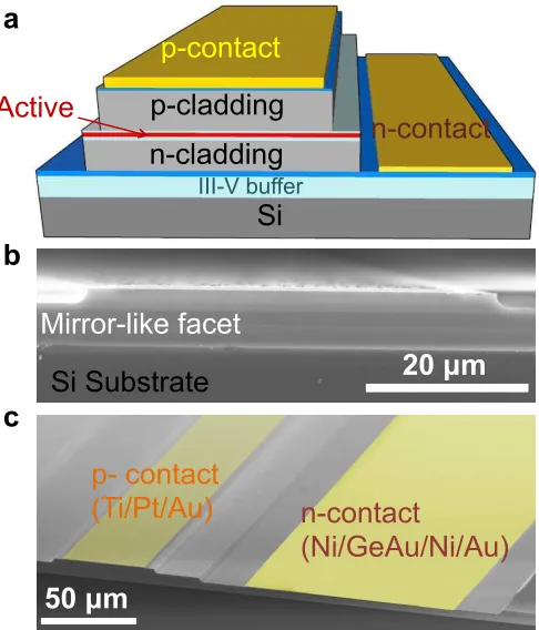
Broad-area lasers were fabricated as shown schematically in Figure 3a. The lasers were processed with as-cleaved facets. A cross-sectional scanning electron microscope (SEM) image of a fabricated InAs/GaAs QD laser on a silicon substrate is shown in Figure 3b. It can be seen that a very clean and mirror-like facet has been achieved. This is important, because imperfectly cleaved facets result in increased mirror loss and reduced differential external quantum efficiency. No coatings were applied to the facets. An SEM overview of a complete III-V laser on silicon is shown in Figure 3c. Laser bars were then mounted on gold-plated copper heat-sinks using indium-silver low melting point solder and Au-wire bonded on the ridge to enable test (Supplementary Information III).
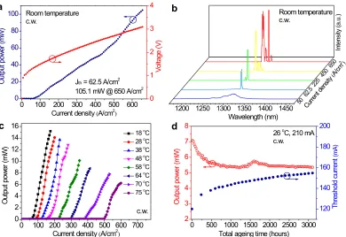
Low Jth and high optical Pout are always desirable goals for laser applications.Figure 4a shows the light-current-voltage (LIV) measurements for an InAs/GaAs QD laser grown on a silicon substrate under c.w. operation at RT. A clear knee behavior in the L-I curve is observed at the lasing Jth of 62.5 A/cm
2
, which corresponds to 12.5 A/cm2 for each of the five QD layers. To the best of our knowledge, this value of Jth represents the lowest c.w. RT Jth for any kind of
laser on a silicon substrate to date, and is comparable to the best-reported values for conventional QD lasers on GaAs substrate13,30. The Pout measured from both facets is as high as 105 mW at an injection current density of 650 A/cm2, with no evidence of power saturation up to this current density.
in the near-field of the laser which evolves with carrier injection (Supplementary Information IV).
In addition to Jth and Pout, for silicon photonic-electronic integration applications, it is important that lasers can operate at high temperature in c.w. mode. This is required because silicon-based electronic chips are often required to work in ambient temperature of 65 oC or even higher, without the use of thermo-electric cooling. Figure 4c shows the c.w. Pout for the QD laser at various temperatures. The c.w. lasing in the ground state was maintained until the testing was stopped at a heatsink temperature of 75 oC due to the limitation of the c.w. current source. This Si-based laser has also been tested under pulsed operation; lasing up to 120 oC is demonstrated with limited self-heating (Supplementary Information IV). To the best of our knowledge, this is the first demonstration of QD lasers directly grown on silicon substrates that lase up to 75 oC and 120 oC under c.w. and pulsed operation, respectively. The characteristic temperature T0 for this device as estimated under pulsed operation is 51 K
between 20 and 60 oC and 35K between 70 and 120 oC (Supplementary Information IV).
A critical requirement for the practical application of electrically pumped lasers on silicon is to achieve sufficient operating lifetime. High reliability, in terms of a long mean time to failure (MTTF) is an important pre-requisite to establish the feasibility of delivering commercial III-V QD lasers directly grown on silicon substrates. Here we present the results from our lifetime study on the InAs/GaAs QD laser epitaxially grown directly on a silicon substrate. The ageing test was performed at a fixed temperature of 26 oC, with the Pout monitored for a constant c.w. drive current of 210 mA (corresponding to 1.75×Ith). Periodic
LIV characterizations were also performed to monitor changes in the lasing threshold. The ageing results are shown in Figure 4d. A 29.7% drop in power, over the ageing test period of 3,100 hours, is observed, with most of the drop (26.4%) occurring in the first 500 hours, followed by a very slow degradation of light output over time. A similar trend was observed for the threshold behavior, in which most of the increase in threshold occurred in the early stages of testing. An extrapolated MTTF (defined by a doubling of the threshold) of over 100,158 hours was determined from fitting the threshold with a sub-linear model (Supplementary Information V)23. It should be noted that these data represent worst case results since (i) the laser was operated epitaxial side up, (ii) the laser was not hard soldered to a high thermal conductivity heat-sink, and (iii) no facet coatings were used. Nevertheless, the estimated lifetime is much longer than the best reported extrapolated MTTF of 4,627 hours for a p-doped InAs/GaAs QD laser grown on Ge-on-Si ÔvirtualÕ substrate23. If the standard industrial techniques described above were used, even better lifetime performance is expected.
The realization of high-quality GaAs-on-silicon layers with low defects, by employing the combined strategies of AlAs nucleation layer, InGaAs DFLs, in-situ thermal annealing and utilizing QDs as laser active regions, developed using the MBE epitaxial growth method, represents a major step towards substituting III-V/Si epitaxy for the III-V on Ge and on Ge-on-Si ÔvirtualÕ substrates. Our results demonstrate that the large lattice mismatch between III-V materials and silicon will no longer be a fundamental hurdle for monolithic epitaxial growth of III-V photonic devices on silicon substrates. In particular, we have achieved c.w. lasing up to 75 oC, with an ultra low c.w. Jth of 62.5 A/cm
2
, a high output power exceeding 105 mW at RT, and a long extrapolated lifetime of over 100,158 hours. Our demonstration of the ability to grow uniform high-quality III-V materials over the whole Si substrate and then fabricate electrically pumped lasers operating in c.w. mode to high temperature, with high uniformity and long lifetime, opens up new possibilities for silicon photonics and for the direct integration of optical interconnects on the silicon-based microelectronics platform.
Methods
plane was used. Prior to material growth, oxide desorption of silicon substrates was performed at 900 ¡C for 30 minutes. Epitaxy was then performed in the following order: a 6 nm AlAs nucleation layer, a 1 µm GaAs buffer layer, InGaAs/GaAs dislocation filter layers, five layers of InAs/GaAs DWELL structures separated by 50 nm GaAs spacers in the middle of a 140 nm undoped GaAs waveguide between 1.4 µm n-type lower and p-type upper Al0.4Ga0.6As cladding layers. Each DWELL structure consisted of a layer of 3-monolayer
InAs QDs sandwiched by 2 nm In0.15Ga0.85As and 6 nm In0.15Ga0.85As. The DWELLs were
grown at 510 ¡C and GaAs and AlGaAs layers at 590 ¡C. Finally, a 300 nm p-type GaAs contact layer was grown.
Device fabrication. The broad-area lasers with 50 µm wide stripes were fabricated by standard lithography and wet chemical etching techniques, the ridge was etched to roughly 100 nm above the active region, to give improved carrier confinement. Ti/Pt/Au and Ni/GeAu/Ni/Au were deposited on p+-GaAs contacting layer and exposed n+-GaAs buffer layer to form the p- and n- contacts, respectively. After lapping the silicon substrate to 120 microns, the lasers were cleaved to the desired cavity lengths and mounted (as-cleaved) onto the heat-sink.
References
1. M. Asghari, A. V. Krishnamoorthy, Silicon photonics: Energy-efficient communication. Nature Photon. 5, 268-270 (2011).
2. A. Rickman, The commercialization of silicon photonics. Nature Photon. 8, 579-582 (2014).
3. L. Virot et al., Germanium avalanche receiver for low power interconnects. Nature Commun. 5, 4957(2014).
4. G. T. Reed, G. Mashanovich, F. Gardes, D. Thomson, Silicon optical modulators.
Nature Photon. 4, 518-526 (2010).
5. R. E. Camacho-Aguilera et al., An electrically pumped germanium laser. Opt. Express20, 11316-11320 (2012).
6. K. Tanabe, K. Watanabe, Y. Arakawa, III-V/Si hybrid photonic devices by direct fusion bonding. Sci. Rep. 2, 349 (2012).
7. Z. Mi, J. Yang, P. Bhattacharya, D. Huffaker, Self-organised quantum dots as dislocation filters: the case of GaAs-based lasers on silicon. Electron. Lett. 42, 121-123 (2006).
8. T. Wang, H. Liu, A. Lee, F. Pozzi, A. Seeds, 1.3-µm InAs/GaAs quantum-dot lasers monolithically grown on Si substrates. Opt. Express. 19, 11381-11386 (2011).
9. A. Lee, Q. Jiang, M. Tang, A. Seeds, H. Liu, Continuous-wave InAs/GaAs
quantum-dot laser diodes monolithically grown on Si substrate with low threshold current densities. Opt. Express. 20, 22181-22187 (2012).
10. A. Liu et al., High performance continuous wave 1.3 µm quantum dot lasers on silicon. Appl. Phys. Lett. 104, 041104 (2014).
11. Z. Wang et al., Room-temperature, InP distributed feedback laser array directly grown on Silicon. Nature Photon.9, 837-842 (2015).
12. Z. Zhou et al., On-chip light sources for silicon Photonics. Light Sci. Appl. 4, e358 (2015).
13. D. Deppe, K. Shavritranuruk, G. Ozgur, H. Chen, S. Freisem, Quantum dot laser diode with low threshold and low internal loss. Electron. Lett. 45, 54-56 (2009). 14. Y. Arakawa et al., Multidimensional quantum well laser and temperature dependence
of its threshold current. Appl. Phys. Lett. 40, 939-941 (1982).
15. M. T. Crowley et al., in Semiconductors Semimetals: Advances Semiconductor Lasers, vol. 86. New York, NY, USA: Academic, ch. 10, 371Ð417 (2012).
16. D. Bimberg et al., Quantum Dot Heterostructures (John Wiley & Sons, Chichester, 1999).
17. G.T. Liu et al., Extremely low room-temperature threshold current density diode
lasers using InAs dots in In0.15Ga0.85As quantum well. Electron. Lett.35, 1163-1165
(1999).
18. M. Sugawara, M. Usami, Quantum dot devices: Handling the heat. Nature Photon. 3, 30-31 (2009).
19. A. D. Lee et al., InAs/GaAs Quantum-Dot Lasers Monolithically Grown on Si, Ge, and Ge-on-Si Substrates. IEEE J. Sel. Top. Quantum Electron. 19, 1901107 (2013). 20. Z. Mi C. et al., High-performance quantum dot lasers and integrated optoelectronics
on Si. Proc. IEEE 97, 1239-1248 (2009).
21. S. F. Chichibu et al., Origin of defect-insensitive emission probability in In-containing (Al, In, Ga) N alloy semiconductors. Nature Mater. 5, 810-816 (2006). 22. R. Beanland et al., Structural analysis of life tested 1.3 µm quantum dot lasers. J.
Appl. Phys. 103, 014913 (2008).
23. A. Liu et al., Reliability of InAs/GaAs quantum dot lasers epitaxially grown on silicon. IEEE J. Sel. Topics Quantum Electron. 21, 1900708 (2015).
25. S. Chen et al., 1.3 µm InAs/GaAs quantum-dot laser monolithically grown on Si substrates operating over 100 C. Electron. Lett. 50, 1467-1468 (2014).
26. H. Liu et al., Long-wavelength InAs/GaAs quantum-dot laser diode monolithically grown on Ge substrate. Nature Photon. 5, 416-419 (2011).
27. M. A. Tischler et al., Defect reduction in GaAs epitaxial layer using a GaAsP-InGaAs strained-layer superlattice. Appl. Phys. Lett. 46, 294-296 (1985).
28. R. Fischer et al., Dislocation reduction in epitaxial GaAs on Si (100). Appl. Phys. Lett. 48, 1223-1225 (1986).
29. M. Akiyama et al., Growth of single domain GaAs layer on (100)-oriented Si substrate by MOCVD. Jpn. J. Appl. Phys.23, L843 (1984).
30. I. Sellers et al., 1.3 µm InAs/GaAs multilayer quantum-dot laser with extremely low room-temperature threshold current density. Electron. Lett. 40, 1412-1413 (2004).
Acknowledgements
The authors acknowledge financial support from UK EPSRC under Grants No. EP/J012904/1 and EP/J012815/1. H.L. would like to thank The Royal Society for funding his University Research Fellowship.
Author contributions
H.L. proposed and guided the overall project with contributions from A.J.S. and P.M.S.. S.C., J.W., A.J.S., P.M.S. and H.L. developed the laser structure. J.W., M.T. and H.L. performed material growth. S.C. and Q.J. carried out the device fabrication and device characterization. S.S., S.N.E. and P.M.S. performed laser near-field measurements and analyses. A.S. and S.S. contributed to the development of device processing. W.L. and I.R. performed TEM characterization and analysis. M.T. and J.W. carried out AFM characterization. S.C., J.W., A.J.S. and H.L. composed the manuscript with input from all co-authors.
Additional Information
The authors declare no competing financial interests. Reprints and permission information is available online at http://npg.nature.com/reprintsandpermissions/. Correspondence and requests for materials should be addressed to H.L.
Competing financial interests
Figure 1. Development and advantages of QD lasers. (a) The historical development of low-dimensional heterostructure lasers showing the record threshold current densities. The red star indicates the threshold value achieved in this work. The blue star is the value normalized to a single QD layer. (b) Schematic of the interaction between QDs and threading dislocations. (c) Bright field scanning TEM images showing the potential interactions between threading dislocations and the QDs.
QD TD
TD
QD
1970 1980 1990 2000 2010 2020
101
102
103
104
105
106
This work Overall Jth
Jth per dot layer QW
QD on GaAs QD on Ge QD on SiGe QD on Si
Quantum Dot
Quantum Well
T
h
re
sh
o
ld
c
u
rr
e
n
t
d
e
n
si
ty
(
A
/c
m
2 )
(l
o
g
)
Year
a
b
[image:9.595.173.428.109.421.2]Figure 2. Epitaxial growth and structural characterization of QD lasers. (a) High angle annular dark field scanning TEM image of the interface between the 6 nm AlAs nucleation layer and a silicon substrate. (b) Bright field scanning TEM image of DFLs. (c) Dislocation density measured at different positions indicated in (b). (d) A PL spectrum for QD active region grown on silicon. The inset in (b) shows a representative AFM image of an uncapped QD sample grown on silicon. (e) High resolution bright field scanning TEM images of a single dot (top-left), corrected high angle annular dark-field scanning TEM images (false colour) of a single QD (bottom-left), and bright field scanning TEM image of the QD active layers (right).
1 2 3 4 5 6
5nm 6 ±0.5nm
GaAs
AlAs
Si substrate
1 2 3 4 5 6 105
106 107 108 109 1010
T
D
D
e
n
si
ty
(
cm
-2 )
(l
o
g
)
Position
a b c
d e
5 nm
[image:10.595.95.498.112.374.2]Figure 3. Fabricated III-V laser directly grown on silicon substrates. (a) Schematic of the layer structure of an InAs/GaAs QD laser on a silicon substrate. (b) A cross-sectional SEM image of the fabricated laser with as-cleaved facets, showing very good facet quality. (c) An SEM overview of whole III-V laser on silicon.
p- contact
(Ti/Pt/Au)
n-contact
(Ni/GeAu/Ni/Au)
Si Substrate
III-V buffer
Si
Mirror-like facet
p-contact
n-contact
n-cladding
p-cladding
Active
b
a
c
20 µm
Figure 4.Silicon laser performance characterization. (a) LIV characteristics for a 50 µm ×
3200 µm InAs/GaAs QD laser grown on a silicon substrate under c.w. operation at 18 oC. (b) Emission spectra for a 50 µm × 3200 µm InAs/GaAs QD laser grown on a silicon substrate at various injection current densities under c.w. operation at 18 oC. (c) Light output power versus current density for this InAs/GaAs QD laser on silicon at various heat sink temperatures. (d) Ageing data for InAs/GaAs QD laser on Si at constant heat sink temperature of 26 oC and c.w. drive current of 210 mA.
0 100 200 300 400 500 600
0 20 40 60 80 100
Jth = 62.5 A/cm2
105.1 mW @ 650 A/cm2
Room temperature c.w. O u tp u t p o w e r (m W )
Current density (A/cm2)
0 1 2 3 4 V o lta g e ( V )
1200 1250 1300 1350 1400 1450
Room temperature c.w. Cur rent den sity (A/ cm 2) 650 450 225 62.5 50 In te n si ty ( a .u .) Wavelength (nm)
0 100 200 300 400 500 600 700
0 2 4 6 8 10 12 14 16
18 o C 28 o
C
38 oC
48 o C 58 o
C 64 o
C 70 o
C 75 o
C O u tp u t p o w e r (m W )
Current density (A/cm2) c.w.
0 500 1000 1500 2000 2500 3000
2 3 4 5 6 7 8
26 oC, 210 mA c.w. O u tp u t p o w e r (m W )
Total ageing time (hours)