ELECTRICAL CHARACTERISATIONS OF PLASMA POLYERMISED LINALYL ACETATE
L. J. Anderson1, M. V. Jacob1*
1
Electronic Materials Research Lab, School of Engineering and Physical Sciences, James Cook
University, Townsville QLD 4811, Australia
*Corresponding author. Tel: +61 7 47814379; fax: +61 7 47815177; Email: Mohan.Jacob@jcu.edu.au
ABSTRACT
Thin films of plasma polymerised linalyl acetate (PLA) were fabricated and their electrical properties investigated. The high frequency dielectric constant was determined using the split post dielectric resonator (SPDR) technique at frequencies of 10 GHz and 20 GHz and compared with the low frequency dielectric constant found from capacitive measurements of metal-insulator-metal (MIM) structures. Dielectric constants of 2.39 and 2.43 resulted from each of the respective techniques, in good agreement with each other. The J-V characteristics of MIM structures fabricated at various RF power levels were then investigated in order to determine the resistivity and DC conduction mechanism of the PLA thin films. From these data, the predominate mechanism of charge transport in the high voltage region was found to be consistent with Richardson-Schottky conduction, and the resistivity of the thin films found to increase with increasing RF power.
1 Introduction
Recently there has been large growth in the industry of organic electronics, as advances in
development and fabrication of organic materials begins to enable the true possibility of fully flexible, large area and low cost devices and components [1, 2]. Organic Field Effect Transistors (OFETs) are an integral component of many organic electronic devices, providing the basis for logic and CMOS circuitry, as well as switching and amplification of signals. Predominantly, research on OFETs is concentrated around the semiconducting channel, where material choice and optimisation, deposition method and post-deposition treatment are heavily explored topics of scientific interest [3-7]. p-Type materials are well explored due to their high mobilities, ease of manufacture and stability in ambient environments [8], and current research has resulted in the properties of n-type materials being greatly improved [5, 9, 10].
When considering the OFET, substrate, electrode and dielectric choice also play a significant role in the overall device performance [11-13]. Currently, investigations into OFETs is commonly performed using bottom-gate, bottom contact or bottom gate, top contact structures on highly doped Si substrates with an SiO2 layer to form the gate and gate dielectric respectively [6, 14, 15]. Metals with a work function well matched to the HOMO / LUMO levels of the organic channel such as gold are then commonly used to complete the device. However, as the benefits of organic electronics and
processing are truly exploited, there will be a need for substrates, dielectrics and electrodes which are flexible and perform as well, if not better than their inorganic counterparts.
Evidence shows that the surface morphology, surface chemistry and dielectric constant of the dielectric layer can influence the overall behaviour of the channel [13, 16]. As well as this, a material’s electrical characteristics are also an important consideration when determining its
suitability as a gate dielectric [13]. Radio Frequency (RF) plasma polymerisation provides thin films which are smooth, pinhole free and void of surface defects [17]. Additionally, plasma polymerised
with a highly disordered, crosslinked structure and allows the development of polymer thin films from materials which are generally un-polymerisable by conventional techniques [20]. One such material, linalyl acetate, a principle component of essential oils such as Lavandula angustifolia, is an
environmentally friendly, non-synthetic material, and in conjunction with plasma polymerisation provides a completely ‘green’ product fabricated via safe and cost effective methods. The benefits of
such films and techniques in industry has been recently discussed by Yasuda [21]. This material has been a subject of recent study into its optical and morphological characteristics [22], as well as its influence over the growth and optical characteristics of an n-type organic semiconductor [23]. Results indicate the potential of plasma polymerised linalyl acetate (PLA) as a dielectric layer in OFET devices. In order to be used as such, a precise understanding of the material properties, such as dielectric constant, conductivity and charge transport mechanisms are required.
In this study, the electrical properties of thin films developed from the non-synthetic, environmentally friendly monomer linalyl acetate have been investigated. The dielectric constant, εr of the PLA material has been derived from two measurement techniques at five different frequencies. These measurements include the Split Post Dielectric Resonator (SPDR) technique at frequencies of 10 GHz and 20 GHz, and measurements of the capacitance of Metal-Insulator-Metal (MIM) structures at 100 Hz, 1 kHz and 10 kHz. Furthermore, J-V characterisations have been performed on MIM samples deposited at varying power levels (10 W, 25 W and 50 W) to determine the conductivity (σ) of the PLA material and the influence of deposition conditions on this value, and the shape of the J-V curves analysed to elucidate the mechanism of DC conduction through the layer. Finally, the optical
bandgap, Eg, of PLA from absorbance data, in agreement with [22], is examined.
2 Materials and Methods
Deposition of PLA thin films took place within a custom made, cylindrical RF polymerisation chamber. The volume of the chamber is approximately 0.0018 m3 at a length of 0.75 m and internal
monomer inlet. The power level used was varied according to the experiment. Two substrates were used during experimentation; the first was quartz glass for measurements using the SPDR technique while for all MIM structures, glass microscope slides were used. Substrates used were ultrasonically cleaned in a solution of doubly-distilled water and Extran for 5 minutes, prior to rinsing in acetone and isopropanol. The substrates were then dried in air and stored in a clean environment. To perform the deposition, approximately 5 mL of linalyl acetate (Australian Botanical Products Pty. Ltd., Australia, used without further purification) was placed in the monomer inlet, and degassed. The substrate was placed in the chamber, and Argon flown through the reactor for 60 seconds to ensure an O2 free deposition surface [24]. At 100 mTorr, RF glow was initiated and the monomer inlet opened once a constant pressure had been obtained. Monomer flow was kept constant via a vacuum stopcock on the inlet. For SPDR measurements, depositions of 100 minutes were performed to obtained samples with an approximate thickness of 1.5 µm. For capacitive measurements, depositions of 30 minutes were performed to obtain samples approximately 500 nm thick. For J-V measurements, depositions of 60 minutes were performed to obtain samples of approximately 700 nm.
For MIM structures requiring metal layers, aluminium electrodes were deposited using thermal evaporation. Patterning was achieved with a purpose made shadow mask placed beneath the samples.
Capacitance was measured using a Wayne Kerr B605 LCR meter, at frequencies of 100 Hz, 1 kHz and 10 kHz. From the measured value of capacitance and device geometry, the dielectric constant, εr, of the PLA layer was determined.
The dielectric constant and loss tangent were determined at high frequencies (10 GHz and 20 GHz) using the SPDR technique [25]. Two TE10δ mode SPDRs with resonant frequencies of 10 GHz and 20 GHz were used to first measure the resonance frequency and Q-factor of quartz substrate with no deposited film (pre-deposition). Subsequent to film deposition, the resonant frequency and Q-factor of the samples were again measured in each of the resonators. From the shifts in resonance frequency
) , ' ( 1 ' f r s f f s r h K f h f f
(1)where fs is the resonant frequency of the SPDR with the substrate only, ff is the resonant frequency of the SPDR with the substrate and deposited film, hf is the thickness of the film and Kε is a function of
εr’ and hf, the value of which is evaluated using the Rayleigh-Ritz technique [26]. Iterative procedures
are then used to evaluate further values of Kε and εr’ until convergence is reached. The loss tangent
tanδ is then determined from (2):
Q QDR Qc
es
/tan 01 1 1
(2)
by measuring the unloaded Q-factor of the resonator, Q0, with and without the sample present, where
QDR-1 is the loss due to the metallic part of the resonator, Qc-1 is the loss due to the dielectric part of the resonator and ρes is the electric field filling the cavity. An Agilent Technologies E8364B network analyser was used to measure the resonant frequency and Q-factor for all microwave measurements. For dielectric measurements at all five frequencies (three audio frequencies and two microwave frequencies), six samples were fabricated, each at an RF power of 25 W. Three samples were deposited on quartz substrates for microwave measurements, and three samples on glass microscope slides for capacitive measurements. The only other differences between these samples relates to the device geometries of the defined MIM structures.
I-V measurements were performed on the MIM structures where the PLA layer was fabricated under RF power levels of 10 W, 25W and 50W using a Keithley 2636A source meter. Measurements were taken between 0V – 200V, and 200 data points measured in this range (step size ~1V). Voltage steps
were used for each point, applied for 80 ms / point, and all currents measured at a current range of 1 µA.
(3)
A multilayer model is then constructed in WVASE32 software, which represents the structure of the sample measured. To obtain thickness values, a modelled glass layer was used as a substrate, with a Cauchy layer directly above it. By performing regression analysis on the Cauchy parameters, the optical properties and thickness of PLA layer was determined. More details on the fitting procedure for PLA thin films are available elsewhere [22].
Optical absorbance data was acquired in the UV-Vis range using an Avantes Avaspec-2048 spectroscopy unit with an Avalight-DHc light source. A background measurement was first
performed, followed by a measurement of a clean substrate with no film deposited to account for the effects of ambient conditions and to determine the absorbance of the sample independently of the substrate. A deposition time of 60 minutes was used to avoid substrate effects reported previously [28]. A MATLAB program was written which converted the measured absorbance data to a Tauc plot and then extrapolated the linear portion of the high energy region to the x-axis to yield optical band
gap values. More details regarding the Tauc relation are available elsewhere [22].
3 Results and Discussion
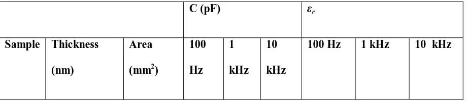
[image:6.595.70.530.637.738.2]Results of the capacitive measurements and corresponding dielectric constants of the PLA material are summarised in Table 1.
Table 1: Dielectric properties of PLA thin films determined from capacitive measurements at low frequencies
C (pF) εr
Sample Thickness
(nm)
Area
(mm2)
100 Hz 1 kHz 10 kHz
100 Hz 1 kHz 10 kHz
1 339.50 12 900 800 767 2.87 2.55 2.45
2 761 20 566 553 543 2.43 2.37 2.33
3 761 18 496 484 475 2.36 2.31 2.26
Average (μ ± σ) 2.55 ±
0.27
2.41 ± 0.12
2.35 ± 0.09
As can be seen from the above data, three MIM structures were fabricated and their capacitance measured at frequencies of 100 Hz, 1 kHz and 10 kHz. From these three devices, a mean permittivity (μ in Table 1) has been determined at each frequency using the measurements obtained from each of the three samples. Standard deviations (σ) have also been included in the table. The trend shows the average dielectric constant is decreasing with increasing frequency, in agreement with other polymer dielectric behaviour such as [29]. Device 1 produced a higher than expected capacitance considering its dimensions; it is believed that there was poor adhesion between the electrodes and the device, and hence a higher contact resistance and interface capacitance contributing to the measured value. Hence the dielectric constant calculated from this sample are slightly high (as are the standard deviations),
however they demonstrate the same expected frequency dependence as other devices and have been included in calculations for completeness.
Table 2 summarises the results of microwave measurements of the dielectric constant of samples at
[image:7.595.70.526.71.242.2]frequencies of 10 GHz and 20 GHz, as well as the associated loss tangent, tan δ, determined from the measurements.
Table 2: Dielectric properties of PLA thin films determined from SPDR measurements at microwave
frequencies
4 2.17 2.57 0.030 0.028
5 2.75 2.10 0.076 0.073
6 2.38 2.40 0.049 0.045
Average (μ ± σ) 2.44 ± 0.29 2.36 ± 0.24 0.051 ± 0.023 0.058 ± 0.023
Again, at each of the two measured microwave frequencies, the average value of εr has been calculated, as well as the average loss tangent. Additionally, standard deviations at each frequency have also been included. The dielectric constant is again observed to decrease with increasing frequency. The reason for the large standard deviation in measured results is attributed to the sensitivity of the SPDR technique. While steps have been taken to ensure the consistency of the experiment, factors beyond control will influence the measurement such as the exact temperature and humidity of the room and slight variations in substrate quality. Given the good agreement between the microwave and capacitive measurements, it is concluded the dielectric constant of PLA is
approximately ~2.4 across a wide frequency range and that the optical measurements performed verify this.
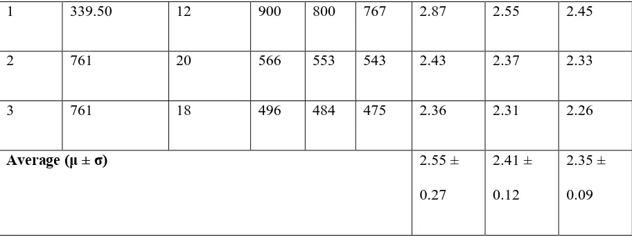
Figure 1: Permittivity estimated from refractive index at optical frequencies
Furthermore, if the refractive index, η, of a sample at optical frequencies is considered [22], the value of the real part of the dielectric function, εr, can be estimated as n
2
[30]. The real part of the dielectric function at optical frequencies is shown in Figure 1, where at long wavelengths εr is again seen to be
~2.4.
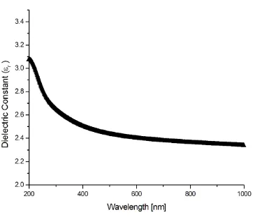
[image:8.595.93.503.71.218.2]Figure 2: J-V measurements of PLA films fabricated at increasing RF power
is very small (< 0.5 mA / m2 increase in current density for a 1 V increase in voltage) and the current is not clearly modelled by one standard mechanism; most likely several mechanisms are contributing to the overall small current until higher fields when one mechanism begins to dominate.
In the high field region several possible conduction mechanisms exist which can be used to model the observed data. The three most likely mechanisms are PF conduction, Richardson-Schottky (RS) conduction and Space Charge Limited Conduction (SCLC) [30, 31]. The PF mechanism describes a bulk limited conduction process, wherein the trap barrier of the material is lowered by the application of a sufficiently high electric field, while the RS conduction describes a barrier limited conduction process, wherein the interaction of an electric field at a metal-insulator interface and the image force induces a lowering of the potential barrier [32]. Both PF and RS process can be described by the generalised equation [33]:
(4)
where J0 is the low field current density, kBis Boltzmann’s constant in eV / K, T is temperature, d is film thickness in m and V is voltage in V. The parameter β is the field lowering coefficient and for PF and RS conduction is given by βPFand βRSrespectively [34]:
(5)
where q is the charge of an electron, εo the permittivity of free space, εr the dielectric constant of the bulk material and the units of β given in eV m1/2 V-1/2. SCLC is a mechanism where a distribution of traps in the bulk material limits the current conducted through the material. Each of these mechanisms can be used to explain the means of conduction in insulators and it is important to determine which effect is dominating charge transport. This can be done by analysing the shape of the J-V curves under different conditions. In the case of PF and RS conduction, plotting ln J vs. V0.5 will provide a linear characteristic, while for SCLC, plotting ln J vs. ln V will provide a linear characteristic. Furthermore,
SCLC for varying film thicknesses should demonstrate a dependence of conductivity on electrode separation. Plotting ln J vs. ln V produced less linear plots than ln J vs. V0.5 and additionally, no film thickness dependence of conductivity was observed and hence SCLC was discounted as the
dominating charge transport effect in PLA films. The J-V characteristics in the high field region (V > 100 V) were therefore modelled from the perspective of PF and RS conduction, using eqn. 4. The result of this modelling is shown in Figure 3.
Figure 3: PF / RS mechanism fit to J-V curves in the high field region
It should be noted that the high field region necessarily includes a region of transition between dominant conduction mechanisms; during fitting the entire ‘high field’ region has been considered.
Additionally, given the complicated structure of plasma polymers, it is likely that more than one conduction mechanism is contributing to the overall behaviour, inducing deviations from a perfectly linear behaviour. It is however evident from the analysis that the PF or RS mechanisms are
dominating and hence these are considered. In order to differentiate between PF and RS mechanisms, the theoretical and experimental values of βPF and βRS can be compared to see which gives the best
agreement [26]. From eqn. 5 and the experimentally determined value of εr of 2.4, the values of βPF
and βRS were determined to be 4.90 x 10 -5
and 2.45 x 10⁻⁵ respectively. From the regression analysis shown in Figure 3, the factor βexp was determined from:
(6)
where m is the coefficient of the linear fit. Experimental values of β are included in Table 3.
From Table 3, βexp is in best agreement with βRS and hence the Schottky mechanism is proposed as the dominate conduction mechanism under high fields. Furthermore the value of βexp remains essentially constant with increasing RF power; given the direct relationship between βexp and εr, this is indicative that εr remains constant with variations in RF power.
Table 3: Summary of PLA electrical properties with εr ≈ 2.4 T
d mkB 0.5 exp
RF Power (W) βexp Eg (eV) σ (pS / cm)
10 1.317 x 10⁻⁵ 3.02 0.382
25 1.325 x 10⁻⁵ 2.96 0.225
50 1.374 x 10⁻⁵ 2.96 0.178
Furthermore, the resistivity of samples with increasing power was determined from the relation
(7)
where ρ is the resistivity, A is the MIM structure’s surface area in m2, d is the device thickness in m and V and I are the measured voltage and current in V and A respectively. The conductivity, σ, has been found for each sample (as the reciprocal of ρ) at 200 V and is shown in Table 3. A clear decrease in conductivity under high field with increasing RF power is observed. This is attributed to the
increase in crosslinking in films fabricated in higher powers, demonstrated previously by chemical and mechanical studies [35, 22]. The order of magnitude of conductivity for all samples is ~10-12 S /
[image:11.595.67.440.71.218.2]cm, placing it in the insulating range [36]. This value is comparable to other plasma polymers, with previous studies on plasma polymerised thiophenes producing films with conductivities in the range of 10-6 S / cm- 10-10 S / cm [36]. The lowest reported conductivity in this study was also found for sample fabricated at higher RF powers, and this decrease attributed to the more amorphous nature of the film. It is also noted that the variation in conductivity in these films was much higher than that observed here for PLA thin films. Plasma polymerised polyaniline thin films have also been reported with conductivities between 10-10 and 10-12 S / cm, and as high as 10-4 S / cm when doped with I2 [37]. Such a drastic increase in conductivity upon the introduction of dopants introduces potential paths for further tuning the conductivity of PLA thin films.
Figure 4: Tauc plot of Absorbance data and determination of the optical band gap d
A I V
Figure 4 shows the Tauc plot determined from absorbance data for samples at 10 W, 25 W and 50 W and the determination of the optical band gap, Eg, by extrapolation of the linear portion to the energy axis. Egfor different films varies minimally with RF power, decreasing from 3.02 eV at 10 W to 2.96 eV at 50 W, corresponding to a 2% variation in Egwith a 40 W increase in RF power. This behaviour is similar to that of the parameter βexp, which also remains relatively constant for films deposited at various powers.
4 Conclusions
The electrical properties of PLA thin films have been investigated using a combination of SPDR, capacitive, J-V and absorbance measurements. The dielectric constant, εr energy gap, Eg and conduction mechanism were found to be constant with all examined RF power levels. The
conductivity of the material shows a decrease for samples fabricated at higher RF power levels. At RF powers of up to 50 W, it seems that the polymerisation process does not differ significantly enough to influence the film structure’s capacity to store charge or change the film’s dominating conduction
mechanism or energy gaps. It is proposed the increased crosslinking of the film at higher RF powers decreases the carrier mobility through the film and consequently increases the resistivity. The low observed conductivity demonstrates that PLA layers could find uses as insulating and blocking layers, where highly resistive, low permittivity materials are required. The dielectric constant of ~2.4 varied minimally across the entire frequency spectrum examined (audio frequencies – optical frequencies), though showed a decreasing tendency with increasing frequency. Combined with desirable optical, morphological properties and chemical stability, tuneable conductivity and low permittivity indicate the potential for the uptake of this non-synthetic, environmentally dielectric material in a wide variety
of flexible, organic electronic devices.
ACKNOWLEDGEMENTS
REFERENCES
[1] S. Logothetidis, Flexible organic electronic devices: Materials, process and applications, Mater. Sci. Eng. B 152 (2008) 96-104
[2] W. Clemens, W. Mildner, B. Bergbauer, New High Volume Applications with Printed RFID and More, Polymer Microsystems 5 (2007) 10-12
[3] M. Yoshida, S. Uemura, T. Kodzasa, H. Ushijima, T. Kamata, High Performance Organic FET with Double-Semiconductor Layers, Synth. Met. 137 (2003) 893-894
[4] K. Kudo, M. Iizuka, S. Kuniyoshi, K. Tanaka, Device characteristics of lateral and vertical type organic field effect transistors, Thin Solid Films 393 (2001) 362-367
[5] B. A. Jones, A. Facchetti, M. R. Wasielewski, T. J. Marks, Effects of Arylene Diimide Thin Film Growth Conditions on n-Channel OFET Performance, Adv. Funct. Mater. 18 (2008) 1329-1339
[6] N. A. Azarova, J. W. Owen, C. A. McLellan, M. A. Grimminger, E. K. Chapman, J. E. Anthony, O. D. Jurchescu, Fabrication of organic thin-film transistors by spray-deposition for low-cost, large-area electronics, Org. Electron. 11 (2010) 1960-1965
[7] T. B. Singh, N. Marjanovic, G. J. Matt, S. Günes, N. S. Sariciftci, A. Montaigne Ramil, A. Andreev, H. Sitter, R. Schwödiauer, S. Bauer, High-mobility n-channel organic field-effect transistors based on epitaxially grown C60 films, Org. Electron. 6 (2005) 105-110
[8] S. Aldrich, Material Matters 2 (2007)
[9] Y. Jung, K.-J. Baeg, D.-Y. Kim, T. Someya, S. Y. Park, A thermally resistant and air-stable n-type organic semiconductor: Naphthalene diimide of 3,5-bis-trifluoromethyl aniline, Synth. Met. 159 (2009) 2117-2121
[10] Y. Kaji, R. Mitsuhashi, X. Lee, H. Okamoto, T. Kambe, N. Ikeda, A. Fujiwara, M. Yamaji, K. Omote, Y. Kubozono, High-performance C60 and picene thin film field-effect transistors with
[11] Y. G. Seol, J. G. Lee, N. E. Lee, Effects of different electroplated gate electrodes on electrical performances of flexible organic thin film transistor and flexibility improvement, Org. Electron. 8 (2007) 513-521
[12] A. Cassinese, M. Barra, M. Biasiucci, P. D'Angelo, Field Effect Devices Based on SrTiO3 Gate Dielectrics for the Investigation of Charge Carrier Mobility in Macromolecular Films, Macromol. Symp. 234 (2006) 1-4
[13] A. Facchetti, M. H. Yoon, T. J. Marks, Gate Dielectrics for Organic Field-Effect Transistors: New Opportunities for Organic Electronics, Adv. Mater. 17 (2005) 1705-1725
[14] J. Haddock, X. Zhang, S. Zheng, Q. Zhang, S. Marder, B. Kippelen, A comprehensive study of short channel effects in organic field-effect transistors, Org. Electron. 7 (2006) 45-54
[15] M. Kotani, K. Kakinuma, M. Yoshimura, K. Ishii, S. Yamazaki, T. Kobori, H. Okuyama, H. Kobayashi, H. Tada, Charge carrier transport in high purity perylene single crystal studied by time-of-flight measurements and through field effect transistor characteristics, Chem. Phys. 325 (2006) 160-169
[16] S. E. Fritz, T. W. Kelley, C. D. Frisbie, Effect of Dielectric Roughness on Performance of Pentacene TFTs and Restoration of Performance with a Polymeric Smoothing Layer, J. Phys. Chem. B 109 (2005) 10574-10577
[17] X. Hu, X. Zhao, A. Uddin, C. B. Lee, Preparation, characterization and electronic and optical properties of plasma-polymerized nitriles, Thin Solid Films 477 (2005) 81-87
[18] C. D. Easton, M. V. Jacob, Ageing and thermal degradation of plasma polymerised thin films derived from Lavandula angustifolia essential oil, Polym. Degrad. Stab. 94 (2009) 597-603
[20 F. F. Shi, Recent advances in polymer thin films prepared by plasma polymerization
Synthesis, structural characterization, properties and applications, Surf. Coat. Technol. 82 (1996) 1-15
[21] H. Yasuda, Y. Matsuzawa, Economical advantages of low-pressure plasma polymerization coatings, Plasma Processes Polym. 2 (2005) 507-512
[22] L. J. Anderson, M. V. Jacob, Effect of RF power on the optical and morphological properties of RF plasma polymerised linalyl acetate thin films, Appl. Surf. Sci. 256 (2010) 3293-3298
[23] L. J. Anderson, M. V. Jacob, M. Barra, F. V. Di Girolamo, A. Cassinese, Effect of a plasma polymerised linalyl acetate dielectric on the optical and morphological properties of an n-type organic semiconductor, Appl. Phys. A, Article Online, (2011) doi: 10.1007/s00339-011-6487-9
[24] I. S. Bae, C. K. Jung, S. J. Cho, Y. H. Song, J. H. Boo, A comparative study of plasma polymerized organic thin films on their electrical and optical properties, J. Alloys Compd. 449 (2008) 393-396
[25] C. D. Easton, M. V. Jacob, J. Krupka., Non-destructive complex permittivity measurement of low permittivity thin film materials, Meas. Sci. Technol. 18 (2007) 2869 1-9
[26] J. Mazierska, M. V. Jacob, A. Harring, J. Krupka, P. Barnwell, T. Sims, Measurements of loss tangent and relative permittivity of LTCC ceramics at varying temperatures and frequencies, J. Eur. Ceram. Soc. 23 (2003) 2611-2615
[27] H. Fujiwara, Spectroscopic Ellipsometry: Principles and Applications, John Wiley and Sons Ltd., 2007.
[28] C. D. Easton, M. V. Jacob, Optical characterisation of radio frequency plasma polymerised Lavandula angustifolia essential oil thin films, Thin Solid Films 517 (2009) 4402-4407
[30] A. A. Dakhel, Mechanisms of dc-current transfer in tris(acetylacetonato)iron(III) films, J. Non-Cryst. Solids 353 (2007) 1529-1533
[31] R. Matin, A. H. Bhuniyan, "Electrical transport mechanism in plasma polymerized 2, 6, diethylaniline thin films," Thin Solid Films 519 (2011) 3462-3467
[32] J. G. Simmons, Poole-Frenkel effect and Schottky effect in Metal-Insulator-Metal systems, Phys. Rev. 155 (1967) 657-660
[33] N. Nagaraj, C. V. Subba Reddy, A. K. Sharma, V. V. R. Narasimha Rao, DC conduction mechanism in polyvinyl alcohol films doped with potassium thiocyanate, J. Power Sources 112 (2002) 326-330
[34] R. Çapan, F. Davis, Electrical properties of a calix[4]acid/amine Langmuir-Blodgett thin film, Mater. Chem. Phys. 125 (2011) 883-886
[35] L. Denis, D. Thiry, D. Cossement, P. Gerbaux, F. Brusciotti, I. Van De Keere, V. Goossens, H. Terryn, M. Hecq, and R. Snyders, Towards the understanding of plasma polymer film behaviour in ethanol: A multi-technique investigation, Prog. Org. Coat. 70 (2011) 134-141
[36] A. Kiesow, A. Heilmann, Deposition and properties of plasma polymer films made from thiophenes, Thin Sold Films 343 (1999) 338-341
Figure 1: Permittivity estimated from refractive index at optical frequencies
Figure 2: J-V measurements of PLA films fabricated at increasing RF power
Figure 3: PF / RS mechanism fit to J-V curves in the high field region