Rochester Institute of Technology
RIT Scholar Works
Theses
Thesis/Dissertation Collections
7-1-1993
Design for manufacturing: Performance
characterization of digital VLSI systems using a
statistical analysis/inference methodology
J. Ignacio Espinosa de los Monteros
Follow this and additional works at:
http://scholarworks.rit.edu/theses
This Thesis is brought to you for free and open access by the Thesis/Dissertation Collections at RIT Scholar Works. It has been accepted for inclusion in Theses by an authorized administrator of RIT Scholar Works. For more information, please [email protected].
Recommended Citation
DESIGN FOR MANUFACTURING:
Performance Characterization of Digital VLSI Systems Using a
Statistical Analysis / Inference Methodology
by
J.
Ignacio G. T. Espinosa de los Monteros
APPROVED
BY:
Pro}.
George Brown.,
M. S.
Thesis Advisor
Dr.
Lynn F. Fuller,
M. S.
Thesis Committee
Prof.
Rob Pearson.,
M. S. Thesis Committee
g/;Z/CJ3
DATE
~/z~
DATE
A
Thesis submitted to the
Faculty of the Computer Engineering Department
at
Rochester Institute of Technology
in partial fulfillment of the requirements
for the degree
of
Master of Science
DESIGN FOR MANUFACTURING:
Performance Characterization of Digital VLSI Systems
Using a Statistical Analysis/Inference Methodology.
I,
Jose Ignacio Gutierrez Topete Espinosa
de
los Monteros,
hereby authorize
the partial reproduction of my thesis by Wallace Memorial Library for
inclusions of brief quotations in reviews or related research, and
not
including related work for commercial use or profit.
Date:
'U!
I(d_1 l1
fThis <M..S. Thesis is
dedicated
to thosemost specialpeoplein
my
life:
(Dr.
Maria
Antonieta
'Espinosa
de Cos Monteros
(my
mother)
Mr.
J. Antonio Qutierrez <T. .
M.
(my
Brother)
jMs.
Maria
tttkna
Tulf$ne.n
(my
girlfriend)
for
theirlove,
understanding, support andbelief
in
me.ABSTRACT
Design For
Manufacturing
(DFM)
is a TQMmethodology
by
whichinherently
producible products canbe
manufactured withhigh
yields,short
turnaround
time and greatflexibility.
Thekey
to the success ofany DFM
programlies
in increasedaccuracy
in themodeling
of theprocess and product
designs,
product simulations and effectivemanufacturing
feedback
ofkey
parametricdata.
Thatis, properly
modeling
andsimulating
designs
withdata
which reflects currentfabrication
capabilitieshas
the mostlasting
influence in theperformance of products. It is this area that is tackled in the
methodology
developed
hereafter;
a methodby
which tofeedback
andfeedforward
parametricdata
critical to the performance ofDigital VLSIsystems
for
performance prediction purposes. In this method, integratedcircuit and applied statistics concepts are used
jointly
to performanalyses and inferences on response variables as a
function
ofkey
processing
anddesign
variables that canbe statistically
controlled.Furthermore,
an experimentaldesign
procedureutilizing
electricalsimulation is proposed to
efficiently
collectdata
and testpreviously
proposed hypotheses. Conclusions are
finally
made with regard to theusefulness and outreach of this method, as well as those areas affected
by
the behavior of the performance predictors,both
in thedesign
andmanufacturing
stagesofVLSI engineering.TABLE OF CONTENTS
ABSTRACT
lvLIST OF TABLES
xLIST OF FIGURES
xiACKNOWLEDGEMENTS
xiiSection
1
-Thesis Principles
11
INTRODUCTION
2
1.1
Introduction
21.2
Problem
Statement,
Objectives
and Hypotheses 41.2.1
Problem
Statement 41.2.2
Objectives
5
1.2.3 Hypothesis
6
1.3 General Assumptions and Justifications 8
2
THEORETICAL BACKGROUND
112.1
SPICE
MOSFETModeling
13
2.2
MOSFET& Circuit
Theory
20
2.2.1
MOSFETs 202.2.2 nMOS
&
CMOS Inverters - DC Characteristics....29
2.2.2.1
The
nMOS Inverter.30
2.2.2.2
The
CMOS
Inverter.
33
2.3
Statistical
Theory
(General
Discussion)
37Section
2
-Methodology
41
3
MANUFACTURING CONSIDERATIONS
423.1
Theory-based Problem Size Reduction
433.1.1
BasicTools
&Techniques
443.1.1.1
Pareto Principle
443.1.1.2
Cause
andEffect Diagrams
453.1.1.3
Machine/System Definition
463.1.2
Application
to the nMOS InverterSystem
493.2
Influential
Processing
Steps'Identification
51
3.2.1
Basic Tools &
Techniques52
3.2.2
Application to the nMOS Inverter System54
3.3
CIM
DatabaseQuery
for Steps &
Variables ofInterest
57
3.3.1 Basic Tools
&
Techniques58
3.3.1.1 MESA Reports and
Control
Charts58
3.3.1.2
AS/400Query Utility
59
3.3.2
Application
to the nMOS Inverter System59
4
PRELIMINARY ANALYSIS
62
4
.1
DescriptiveStatistical
Analysis ofRaw Data62
-vl- J.Ignacio
4.1.1
Basic
Tools &
Techniques
62
4.1.2
Application
to the nMOSInverter System
64
4.2
Capability
Analysis
of theData
65
4.2.1
Basic Tools
&Techniques
664.2.1.1
Metrology
Characterization
66
4.2.1.2
Gauge
Capability
674.2.1.3
Capability
Determination
704,2.
1.4Problems
andSolutions Associated
withAcademic
Manufacturing
Environments..
794.2.2
Application
to the nMOSInverter System
825
I
DESIGN CONSIDERATIONS
865.1
VLSIDesign Evaluation
86
5.1.1
Concepts
865.1.2
Application
to the nMOS InverterSystem
875.2
Layout
Parameter Extraction(LPE)
88
5.2.1
Concepts 915.2.2
Application to the nMOS InverterSystem
92
6
STATISTICAL
EXPERIMENTATION
956.1
Design ofExperiment(s) (DofE)
95
6.1.1
Background Information96
6.1.1.1
Introduction to DofE96
6.1.1.2 Statistical Experimental Designs 97
6.1.1.3
Hypotheses Determination
996.1.2
Application
to the nMOS InverterSystem
996.2
SPICECalculations
andSimulation
Runs 1026.2.1
Associated Tasks
1036.2.2
Application
to the nMOS Inverter System 1046.3
Analysis
ofResult
Set(s)
1086.3.1
Basic
Tools & Techniques 1086.3.2
Application to the nMOS InverterSystem
1107
MANUFACTURABILITY ASSESSMENT
1147.1
ProductFunctionality,
Manufacturability
&
OtherImplications 114
7.1.1 Concepts to Consider. 114
7.1.2 Application to the nMOS Inverter System 116
Section
3
-Final Notes
1198
SUMMARY,
CONCLUSIONS&
RECOMMENDATIONS 1208.1
Summary
1208.2
Conclusions 1228.2.1
Regarding
TheMethodology
1228.2.2
Regarding
The CaseStudy
1258.3
Recommendations 129REFERENCES
131BIBLIOGRAPHY
133APPENDIX A
Guggenheim
Wafer
Sizing
Machine Definition
135APPENDIX B
Theory-
based
Reduction to Vital FewCauses for
thenMOS Inverter's Performance 145
APPENDIX
C
RIT nMOS Process v.
2
.0 InstructionsListing
157
APPENDIX D
nMOS
2.0
MESA Database Control Charts 161APPENDIX
E
Statistical Description &
Capability
Analysis ofnMOSv. 2.0 Process Measurements 165
APPENDIX
F
VLSI
Layouts,
CircuitsDiagrams,
HSPICE Netlists andSimulation Results 188
LIST OF TABLES
1
Empirical
Model HSPICE Parameters
152
MOSFET
Characteristic
Equations
ofRelevance 283 nMOS
Inverter Characteristic Equations
314 Voltage
Relationships for
theCMOS
Inverter'sRegions of
Operation
345
nMOSInverter
Performance: The Vital Few Causes51
6 Recommended Sample
Sizes
for
Short &Long
TermCapability
Studies 787 E-Mail Warnings From
Quality
Control Expert 818 Geometric Values
for
E/D Inverter Chosen 939 B-B Design
for
Use in Simulation Framework 10110 Values
for
the Three-levels ofthe Three-factorsBeing
Considered 107
11 Methodology's Simulation Results 110
12
Methodology Summary
122LIST OF FIGURES
1
Thesis
Overview
72
MOSFET Physical Structures
20
3
Enhancement
versusDepletion MOSFETs
21
4 I-V
Characteristics
for
n-&
p-transistors24
5
nMOSDevice
Conducting
Channel
Behavior.
256 nMOS
Inverter
BasicStructure
30
7 nMOS
Inverter
Characteristic
Curves
32
8
CMOS Inverter.
34
9
Graphical Derivation
ofCMOS
Inverter's DCTransfer
Curve &
Operating
Regions
3510
C-and-E Diagram for
ProcessGain,
p
4611
Machine /System
DefinitionSummary
4812
InstrumentAccuracy
Deviations Possible69
13 Skewness 73
14 Kurtosis 74
15
Machine/Process Potential76
16 Machine /Process
Capability
7717 E/D Inverter as Depicted
by
H. J. Bijker 89Xl - J. Ignacioq. 7.
ACKNOWLEDGEMENTS
First
of all, I wouldlike
to thankGOD
for
the skills andopportunities that I
have
been
given and those successesI have been
ableto accomplish in
my
life
sofar.
The
complexity
ofthisstudy
has
involvedhelp
from
several peoplewith the traits and
knowledge
that I needed in order tolearn
severalconcepts and thus
be
able to complete thedifferent
subjects that arediscussed hereafter.
They
include: First ofall,Professor George
A. Brownof the
Computer
Engineering
Department
atR.I.T.
Thanks
tohis
tutelage
I have been
able to growintellectually
and thanks tohis
comments and explanations I
have been
able to complete thisdocument.
Second,
Dr. Lynn F.Fuller,
head of theMicroelectronic
Engineering
Department at R.I.T. Withouthis
experience,knowledge
ofthe subject, and classroom teachings I would not
have been
able to comeup
with the ideas behind thisdocument.
Also,
withouthis
continuedsupport thisproject would
have been discarded
long
ago.Finally,
I wouldlike
to thank all those who touchedmy
life
inany
way
during
my
academiclife
atR.I.T, especially
Dr. John T. Burr of theCenter for
Quality
and Applied Statistics. Without those experiences,and inleiieclueii encounters
I
wuuidhave suieiy
gone in adifferent
direction.
- Xll
S/S>
ff^ 4=.
^s=rv^7 !Thesis Principles
INTRODUCTION
1.1
Introduction
Design
for
Manufacturing
(DFM)
is amethodology
by
whichinherently
producible products canbe
manufactured withhigh
yields,short turnaround time and great
flexibility.
There are several ways toachieve these objectives.
One
suchway
isby
reducing
variability
levels infabrication
processes and thus increase capabilities on the individualprocess steps, as well as whole processes
for
mass production.Another
way
to attain this isby
realistic characterization ofprocesses,leading
to models which canbe
used at the circuitdesign level
in order to preventviolations of physical and electrical rules that could
hinder
performanceofthe overall system.
The
key
to the success ofany
DFM programlies
in increasedaccuracy
in themodeling
of the process and productdesigns,
productsimulations and effective
manufacturing
feedback
ofkey
parametric data. It is this area which proves most effective whendealing
with theinteractions
between manufacturing
anddesign.
That
is,
properly
modeling
andsimulating
designs withdata
which reflects currentfabrication
capabilities has the mostlasting
influence in theperformance ofproducts.
This
has
been
the motivationbehind
geometric(drawn)
rulegeneration and electrical parameter extraction
for very large
scaleintegrated
(VLSI)
systems.Even
thoughcorrectly
drawn
structures arenecessary for integrated
(semiconductor)
circuits to attain thedesired
topology,
electrical characterization anddevice
parameter extraction areindispensable to predict actual performance ofthe product.
The
Simulation
Program for Integrated
CircuitEngineering
(SPICE)
has
long
been
regarded as essential in the simulation ofdigital
andanalog
circuits ofany
sort,both academically
and industrially. Thisprogram
has
theflexibility
to choosebetween different
models andfill
out as
many
parameters asnecessary for
thedesired accuracy
level.Moreover,
it will take into consideration the interconnection structure ofthe system and will interrelate the inherent device physics that underlie
the elements which compose it.
Other tools which have
recently
become available to those in thearea of DFM includes statistical analysis. Statistics has
successfully
been
used in various disciplines. This has allowed the use of morestringent control and specifications,
making
processes and products more reliable and reproducible than everbefore.
Nevertheless,
techniques like those ofdescriptive statistics,
capability
analyses, designofexperiments and statistical process control
(SPC)
arevery
new to thoseworking
in the semiconductor industry.1.2
Problem
Statement,
Objectives
andHypothesis
Variability
is inherent toany
manufacturing
process.Quality
is afeature
that ishard
to attain, and evenharder
to maintain. RochesterInstitute
ofTechnology
has
made it one oftheir goals to "make studentsmore aware of
high-quality
engineering
andmanufacturing"
so as "to make the companies graduates work
for
more competitive in the world market."[4]With
thisfive-year
goal in mind, the student-run integrated circuit(IC)
factory
should undergo acurrent-capability
analysis in order to assess what specific objectives will allow the achievement ofthe goalstated above. This subsection will consider the general problem
being
faced
by
design
andmanufacturing
efforts, as well as the desiredobjectives and
hypotheses
that mustbe
provided.1.2.1
Problem Statement
Precision,
accuracy,quality
andreliability
andhigh
performanceare goals that
both
VLSI designers and IC manufacturers have in common. The metricsfor
these goals can be in theform
ofhigh-yield,
low
turnaround time lowest cost objectives, as well as in theform
ofhigh-performance, low-power,
short time delay. Whateverthey
may be
called,
they
are genuine concerns that affect the relationshipsbetween
both
sides of the overall process which results in semiconductorelectronic systems.
Nevertheless,
the way to achieve these objectives is notwell understood.To begin with, designers need proper characterization of
devices
and well-defined parameters in order to
design
according
to realistic constraints and specification limits within which the systems will workproperly.
On
the otherhand,
manufacturers have theeverlasting
nuisance of
dealing
with the idealistic andhighly
controlled conditionsin which
designers
simulate,verify
and test systems tobe
manufactured;this is a set of circumstances that
rarely
occurs in reality. There isobviously
alack
ofdetailed
andtimely
communicationbetween
the twoparts that make
up
the entire process.Acomparison
between design-side
and manufacturing-side resultsis necessary. These results are to
be
thoroughly
analyzed.Furthermore,
characterizations of the performance that is supposed to
be
attainable and that isactually
obtained shouldbe
compared.Finally,
recommendations willbe
made to close thegap
between
the ideal designand the actual product in
future
efforts. A means to visualize the method that needs tobe
used to solve this problem willbe
providedthrough the detailed application of this procedure to a product
(design)
at the R.I.T. Fab.
1.2.2
ObjectivesThis
study
intends to concentrate on the feedback pathexisting
from
themanufacturing
stage to the design stage.A
method willbe
developed
by
which tools such as SPICE will provide realistic indicatorsofthe attainable performances
from
the targetmanufacturing
conditions under which the VLSI systems willbe
fabricated. This will include adetailed
analysis ofthe interactions between each ofthedifferent factors
that affect thisfeedback,
as well as techniquesfor
obtaining
the mostsignificant results out of the information available
for
characterization of the fabrication processes that affect designsrunning
through them.Moreover,
recommendationsfor future
work willbe
drawn from
theresults obtained out ofthis methodology.
Because
ofthelarge
span of variables that affect thefeedback
from
fabrication
todesign,
there needs tobe
somekind
ofcontrol in order tobetter
understand the most important ones.Theoretical background
from
both
stages of the production process willbe
used to reduce thetotal set of variables to the maximum extent possible,
by
understanding
the relationships
between
all of them.Statistical
tools ofanalysis andinference will
be
used todefine
the subset of interactions which cancurrently
be
studied and which will produce thelargest
resultsamong
those variables available
for
study.Finally,
there is a needfor
examples of the usefulness of thismethod is noticed.
Therefore,
a simple application ofthis method to thenMOS inverter will
be
considered, results willbe
outlined andconclusions stated in order to foresee practical uses of this method and
possible expansion of it into other areas that affect the relationships
between
manufacturing
and design.1.2.3
HypothesisWith all the
tools,
techniques andtheory
available, a solution isproposed. This solution specifies a set of steps
by
whichmanufacturing
data
can influencedesign
work, as well asfactors
such as cost and yield.This is shown in figure
1
(page 7 above). It canbe
seen that the natureof the interactions between
manufacturing
anddesign
is complex, nomatter how simplified the model
may be.
Themethodology
tofollow
<U
I
os o u +-) cu CU co o aCO ^^ CU
5,
UJ cu .3a.
*
S-i O<u
&
U o n>
oCUCU a H C 4> o co Cu 4-1 CU 2 CU 3
0
V
v
t o *-> 4-1 CO 3 o CO u c (33 O u. H2
cC tlfl
*
*P
^ CO CI CU > CU
gQ
-J *-4 1 CU cu > -> cu co JO
oL
c o 4-1 o2
4^ x u u cu 4-1 CUs
CO u CO CuU
a
CU a CO C 0 (Ua
u 4-1 CO * COH
aCOw u
<u 4-1
F-s
o cua
l/J CO CU OS CO 4-1 COQ
< ' eo C 4W ttDCBM ?U (8
3
S9
8J X c CO 2 ^^ c o 03 CO 1 0)0
2
> u V 4W *-> CO + u u ffi UJ t c u uU ECu CO
co a. 2o
a
3
T3 cu co 4J CO cu 4-1s
s
cu<4- 4WCU o 3 CO
s ^ 4-> o cu 3 4-> 3 o (0 u u T3 O s-u u A Cu (0 U. o (Tl 4-1 4-1 s
S
Q
4-1 cu 4->3 CO n a >> n c C/J o cu OT7 CO u> n CO 0. (Tl .o
*
s 4-1cou O 0 4-1 co
a
4-i3 co
5
4-1 X UJ a T3 c co >> 3 co o 4-> CO _, CO
5
(i) cu cu a T3 4->a
2
cfl c CO acu CO
Q
3 (Tl o <4-l 4->
Q
o cos:^
-J*2
co X (3 >
u. O
+i
4J
5
oa CUza CO
Xl CO H
CO a CO
1
C/l U%
involves analysis and manipulation of
data
inboth
manufacturing
anddesign.
It
is important to notice that the major emphasis of this modelis in circuit performance characterization. This is
why
there isonly
aweak
link between
manufacturing
anddesign
involving
layout design
rules.
It
is most important to notice the series of steps required ratherthan the work involved in each ofthem.
This
isbecause
one ofthe goalsof this
study
is tobe
able to expand thisreasoning
into moredetailed
research as well as into other areas that affect the relationships between
fabrication
anddesign
work. Thehypothesis
is that this method worksand can
be
used to simulaterealistically
any
effects ofmanufacturing
variability
at thedesign
stage, thereforereducing
theprobability
of productfailure
oncefabrication has begun.
Moreover,
it ishypothesized
that the effects of machine and process capabilities canbe
accountedfor
at
design level
in order to reduce the aftermath of problems thatmay
occurotherwise.
1.3
General
Assumptions
andJustifications
The
material and methodhere
presented arelargely
simplifieddue
to the real size ofthe problem
being
dealt
with here. The true size andquantity
of relationships that exist betweendesign
andmanufacturing
are too
many
to handle in a single effort of the size of this one.Thus,
some assumptions and justifications are given in order to
better
understand the problem space that willbe
coveredby
the solutionbeing
proposed
hereafter.
The
first
assumption is that thelayout design
rules that providegeometric
data
(which
defines
areas of capacitive and resistiveimportance)
areheld
true.That is,
their effects on performance will notbe
tested and theirvalidity
will notbe
questionedfor
the purposes ofthis research.The
justificationbehind
this is that the number of variablesthat can therefore
be held
constant will increase and the problem spacewill converge into a more manageable one.
Otherwise,
Interactions that occurdue
to thegeometry
ofstructures asfar
as performance anddevice
parametrics are concerned would make the problem
far
too complex.This implies a need to investigate what effects
geometry
considerationswill
have
on performance when variations in sizes come toplay
after themanufacturing
process. This isbeyond
the reach ofthis research.Another assumption that is made refers to the sole use of SPICE
as a characterization tool. There are
many
more tools that canbe
used to characterize circuits.Nevertheless,
SPICEhas
been
regarded as astandard throughout academic and industrial environment. The models contained in this package are thorough enough
for
the purposes ofthis project. Even though there aremany
models, the treatmentwillonly
be
made at an empiricallevel.
Certainly
there are other more involved and thorough models toconsider, butdue
to the simplifications that are sure to exist in thisstudy
the needfor
such models is somewhat irrelevant.A
third assumption considered here is thatcapability
studies, as important asthey
are to thefactory
environment, come intoplay
to determine the variability that is relevant to those causes which affectperformance in
any
way.Certainly,
complete studies ofthis sort wouldprove more
insightful
and could showhow
to improveaccuracy
andprecision in mass production.
Nevertheless,
thebroad
nature of thisresearch cannot concentrate on this matter alone and must consider
only
those results which are of importance to the overall circuit performance assessment as related to thevariables under study.Another
assumption that isbeing
usedhere
is that ofthe limitedextent of
knowledge
that canbe
used asfar
as Statistics and Design of Experiments is concerned. This willcertainly have
the effect ofsimplifying
matters more than if more thoroughknowledge
regarding
suchdisciplines
was available.Nevertheless,
the analysis, inferencesand results obtained
from
the use of thisdisciplines
will be robust in their nature and should not misleadfuture
efforts in this area ofresearch.
Finally,
even though there aremany
tools availablefor
the circuitsbeing
studied,only
those which aremostly
encountered at RochesterInstitute of Technology's Computer
Engineering
and MicroelectronicEngineering
departments willbe
considered. The reasonfor
this is thatthe
lack
of technical support could result in serious setbacks, animpossibility
to complete thestudy
and could even make the conclusionsbecome
unreliable due to theinability
to prove the usefulness of themethodology developed in theory.
THEORETICAL
BACKGROUND
Parameter
extraction is avery
important part ofany
successfulDFM
effort.It
is recognized that without accurate models usedby
designers
ofVLSI
structures,faulty
products result and variationremains out of control throughout the process. It is of particular interest
for designers
tohave
reliable measures ofquality from
themanufacturing
side,especially
in a quantitativeform
usable within the models available.It is
because
of thisreasoning
that tools such asSPICE,
weremade available.
SPICE
wasfirst developed
at theUniversity
ofCaliforniaat
Berkeley
with the goal ofanalyzing
integrated circuitsby
simulating
models
containing
parameters which demonstrate the effects ofmanufacturing
process changes on circuit performance.Furthermore,
itbecame
a standard whichhas
played a central role in thedevelopment
ofproprietary
and commercial tools of similar,but
enhancedfeatures.
Tools such as the Mentor Graphics'
Accusim,
Meta-Software's HSPICEand others
have
become more common nowadays.Some
toolshave
become
more accepted than others,making
itdifficult
to choseamong
them. Due to its similarity to the original
SPICE,
itscompatibility
toCAD
tools currently used, and its straightforward
operation HSPICE is agood example ofintegrated circuit
modeling
software tools thathas been
well accepted in the
engineering
world.Selection
by
designers
of the correct model within the program isessential
for
validation of the workdone
prior tomanufacturing
procedures.
Several
models exist within each of the tools that canbe
chosen
for
particular applications.Most
frequently,
corporations willhave
their own circuit modelsfor
use in simulators and validation tools.In
the academic world, on the otherhand,
models inherent to theprogram are accepted as such, unless research
has been
conducted tofind
more accurate ones.In this particular study,
due
to itsfocus,
as well as its approach, asimple model will prove
very helpful
insimplifying
themethodology
being
developed. Problems associated with more complex models, as well as
the inclusion of
large
numbers of parameters within a particular modelwill
be left for future
research efforts to solve.Therefore,
an empiricalmodel
has been
chosenfor
use in themethodology
that willbe discussed
in the
following
chapter.Integrated circuits are quite complex in their behavior and the
ways to understand them. Most of the
design
world looks at VLSIstructures as sets of switches with a number of resistances and
capacitances which hinder their performance.
Nevertheless,
theindividual
"switches"
are
dealt
with in avery
simplistic manner. On theother
hand,
themanufacturing
world regards these structures ascomplex electromagnetic
"machines"
which are composed of elements
rather complex themselves. This
discrepancy
between
the two worldshas
made a
large
impact In the development offeedback
linesfrom
manufacturing
to design in order to reduce variation in thecharacteristics of circuits, increase yield, turnaround
time,
etc.Obviously,
there
is a needfor
a middle groundbetween both
views.In this chapter it is
intended
to provide abroad
enough set ofconcepts to provide
for
abasis from
which to extract thenecessary
toolsfor
method-building
and analysis essentialthereafter.A
knowledge
baseis
drawn
from
avery diverse
number of places,centering
aroundSPICE
modeling. These include software modeling, such as that used in
SPICE,
MOSFET
theory,
Inverter circuittheory,
Statistics
(Descriptive andAnalytical),
Design ofExperiments, manufacturing
issues such as yield,cost of
ownership
and others whichare impactedby
the performance andmanufacturability
of the circuits processed in the VLSI industry. All ofthe cohcepts that are
necessary
in order to understand themethodology
developed
and explained in subsequent chapters isdiscussed below.2.1
SPICE
MOSFET
Modeling
Transistors,
whether pMOS or nMOS,have
a number ofcharacteristics which are
becoming
more and more importantto considerin order to achieve the speeds and densities which are
currently
soughtafter. Their
modeling
is essentialin order toproperly
predictbehaviors
of small and large structures as well asbe
able to assess the speed and power dissipation desiredfor
the VLSI productbeing
designed. SPICE contains models that are accurate and thorough enough tofulfill
theneeds of
both
design and fabrication.Also,
it canfully
characterize the elements which are so essential to performance inIC
circuits.Moreover,
it provides the tools to simulate
larger basic
elements, such as
inverters,
which
define
the essential structure which alldigital
circuits in integrated circuitdesign
canbe
reduced to in the end.SPICE's
empiricalmodel
(level
3)
contains a number ofparameters whichhave both design
andfabrication
theory
behind
them.Because
ofthis reason, a generaldiscussion
of each ofthose parameters and theirtheory
are essential to thebetter
understanding
ofthe methoddiscussed
subsequently.For VLSI
applications of programslike
HSPICE,
circuit models aredefined
by
theMOSFET
model and element parameters, and twosubmodels selected
by
theCAPOP
(MOSFET gatecapacitances' model)
and ACM (Area
Calculation
Methodfor bulk diode
modeldetermination)
parameters[
1 ].The
selection ofthe MOSFET model typedepends
on the electrical parameters critical to the application. In this case, the number of parameters is tobe
reducedsubstantially
totry
out the method of interest to the minimumfew
requiredfor
meaningfulness.The MOS transistor is described
by
use of an element and a.MODEL statement (just as in SPICE). The element statement
defines
theconnectivity
of thetransistor,
as well asreferencing
the .MODELstatement. The .MODEL statement defines the transistor operation as that of an n- or p-channel
device,
itslevel
and other modelparameters of interest. The CAPOP parameter is associated with the MOS model.Depending
on itsvalue, different capacitor models are used to model the MOS gate capacitance.Modeling
ofthe bulk-to-source andbulk-to-dram
diodes
are selectedby
theACM
parameter, which controls thegeometry
ofthe source and drain
diffusions,
resistance, capacitance and DCcharacteristics
[1].
There
areintricate details
concerning
the correct useof each of this
modeling
options and submodels, which areleft
to themanuals to explain in a more
thorough
manner.The CAPOP
andACM
parameters will
specify
the set of equations to use in the calculation ofcapacitances, resistances and areas of importance. This
feature
is ofimportance
in themethodology
explained in chapter3,
since some ofthese parameters need to
be held
constant somehow and this provides asimple method
for
doing
so.Certainly,
different
processes willhave different
emphases ondifferent
variables availablefor
modeling.Nevertheless,
having
anempirical (level
3)
model there are certain parameters thatbecause
oftheir
importance,
need abrief
explanation.These
are shown in table 1along
with a shortdefinition,
default
value and units usedfor
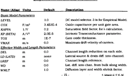
each of [image:28.543.52.490.420.675.2]them.
Table 1
Empirical Model HSPICE Parameters
Name (Alias) Units Default Description
BasicModel Parameters
LEVEL
COX
KAPPA
KP(BETA)
TOX
VMAX
F/m2
1/V
A/V2
m
m/s
EffectiveWidthandLength Parameters
DEL
LD
(LATD)
LREF
WD
WMLT
m
m
m
m
1.0 DC modelselector.3isfor Empirical Model. 3.453E-4 Oxide capacitanceperunitgatearea.
0.2 Saturation field factor,for Xcalculation.
2.0E-5 IntrinsicTransconductance parameter.
1E-7 Gate oxidethickness.
0.0 Maximumdrift velocityof carriers.
0.0 Channel lengthreduction on each side.
none Lateralsource& drain diff. intochannel. 0.0 Channellengthreference.
0.0 Lat. diff. intochan. from bulkalongwidth.
1.0 Diffusionlayerand width shrink factor.
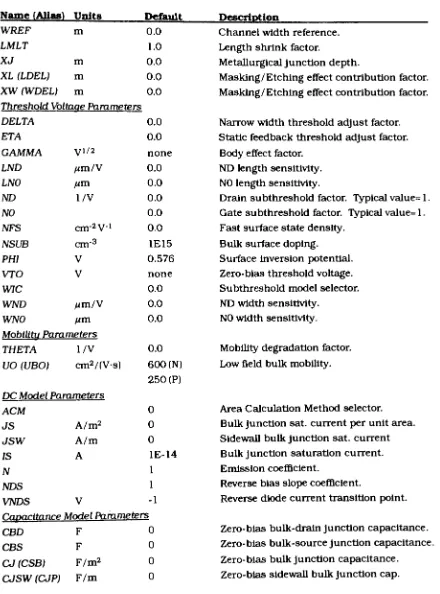
table
1
(continued)
Name (Alias) Units Default Description
WREF m 0.0
LMLT 1.0
XJ m 0.0
XL
(LDEL)
m 0.0XW(WDEL) m 0.0
Threshold Voltage Parameters
DELTA 0.0
ETA 0.0
GAMMA V1'2
none
LND fxm/V 0.0
LNO nm 0.0
ND 1/V 0.0
NO 0.0
NFS 0.0
NSl/B cm-3 1E15
PH/ V 0.576
VTO V none
WIC 0.0
WND fim/V 0.0
WNO nm 0.0
MobilituParameters
THETA 1/V 0.0
UO(UBO) cm2/(Vs) 600(N)
250(P)
DC ModelParameters
ACM 0
JS A/m2 0
JSW A/m 0
IS A IE-14
N 1
NDS 1
VNDS V -1
CapacitanceModelParameters
CBD F 0
CBS F 0
CJ(CSB) F/m2 0
CJSW
(CJP)
F/m 0Channelwidthreference.
Lengthshrink factor.
MetallurgicalJunction depth.
Masking /Etching
effect contribution factor.Masking/
Etching
effectcontribution factor.Narrowwidththresholdadjustfactor.
Static feedbackthreshold adjustfactor.
Body
effectfactor.ND lengthsensitivity.
NOlengthsensitivity.
Drain subthresholdfactor. Typicalvalue=1.
Gate subthresholdfactor. Typicalvalue=1.
Fastsurface statedensity.
Bulksurfacedoping.
Surface inversion potential.
Zero-bias thresholdvoltage.
Subthresholdmodelselector.
NDwidth sensitivity.
NOwidth sensitivity.
Mobility
degradation factor.Lowfield bulkmobility.
Area Calculation Methodselector.
Bulk junctionsat.currentper unit area.
Sidewall bulk junction sat. current
Bulkjunctionsaturation current.
Emissioncoefficient.
Reverse biasslope coefficient.
Reversediode currenttransitionpoint.
Zero-bias bulk-drain junctioncapacitance.
Zero-bias bulk-source Junctioncapacitance.
Zero-biasbulkjunction capacitance.
Zero-bias sidewallbulkjunctioncap.
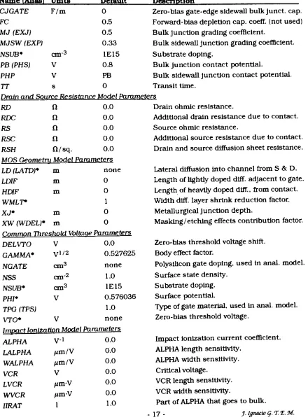
[image:29.543.56.496.63.657.2]table
1
(continued)
Name(Alias! Unite Default Description
CJGATE FC MJ (EXJ) MJSW(EXP) NSUB* PB(PHS) PHP TT F/m cm" V V s 0 0.5 0.5 0.33 1E15 0.8 PB 0
Zero-biasgate-edgesidewallbulkjunct. cap. Forward-biasdepletioncap. coeff. (notused) Bulkjunction gradingcoefficient.
Bulksidewalljunction gradingcoefficient. Substrate doping.
Bulkjunction contact potential.
Bulksidewalljunctioncontact potential. Transittime.
DrainandSourceResistanceModelParameters RD RDC RS RSC RSH P. n n p. ft/sq. 0.0 0.0 0.0 0.0 0.0
MOSGeometryModel Parameters LD(LATD)*
m none
LDIF m 0
HDIF m 0
WMLT* 1
XJ* m 0
XW(WDEL)*
m 0
Common Threshold Voltage Parameters DELVTO GAMMA* NGATE NSS NSUB* PHI* TPG (TPS) VTO* V yl/2 cm" cm cmJ -2 0.0 0.527625 none 1.0 1E15 0.576036 1.0 none Impact IonizationModel Parameters ALPHA LALPHA WALPHA VCR LVCR WVCR IIRAT V-l jim/V fim/V V /mvV /mi-V 1 0.0 0.0 0.0 0.0 0.0 0.0 1.0
Drainohmic resistance.
Additional drain resistancedue to contact. Sourceohmlc resistance.
Additional source resistancedue tocontact. Drainand sourcediffusion sheet resistance.
Lateral diffusion intochannel from S &D. Length of
lightly
dopeddiff. adjacenttogate. Lengthofheavily
dopeddiff., fromcontact. Widthdiff. layershrinkreductionfactor. Metallurgicaljunctiondepth.Masking /etching
effects contribution factor.Zero-biasthresholdvoltage shift.
Body
effectfactor.Polysilicongatedoping,used Inanal, model. Surfacestatedensity.
Substrate doping. Surface potential.
Typeofgate material,usedinanal, model. Zero-biasthresholdvoltage.
Impactionizationcurrent coefficient. ALPHA length sensitivity.
ALPHAwidth sensitivity. Criticalvoltage.
VCRlengthsensitivity. VCRwidth sensitivity.
PartofALPHA thatgoesto bulk.
[image:30.543.56.496.82.682.2]table
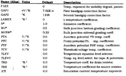
1
(continued)
Name(Alias) Units Default Description Basic GateCapacitanceParameters
CAPOP 2
COX(CO)* F/m2
3.453E-4 TOX*
m 1E-7
Gate
Overlap
CapacitanceModel Parameters CGBO(CGB) F/m 0.0F/m 0.0 F/m 0.0 m none m 0.0 m 0.0 CGDO(C2) CGSO(CI) LD(LATD)* METO WD*
Capacitancemodelselector. Oxide capacitance perunit area. Thin oxidethickness.
Gate-bulk overlapcap./meterchan. length.
Gate-dram overlapcap./meterchan. width. Gate-source overlapcap./meterchan. width Lateral diffusion intochannel from S & D.
Fringing
field factor forG-to-S& G-to-D capLat. diff. Intochan.from bulk alongwidth. MeuerCapacitance Parameters. CAPOP=0.1.2
CF1 CF2 CF3 CF4 CF5 CF6 CGBEX 0.0 0.1 1.0 50.0 0.667 500.0 0.5
ChargeConservation Parameter. CAPOP=4
XQC 0.5 NoiseParameters AF 1-0 KF 0.0 NLEV 2.0 GDSNOI L0
Temperature EffectsParameters
BEX -L5
CTA 'K1 0.0
CTP "K1 0.0
EG eV 1.11(TLEV=0,1)
1.16(TLEV=2)
-
18-Modif. MEYERcntrl. forcgstransition from
depletionto weakinversionforCGSO. Modif.MEYERcntrl. forcgstransitionfrom
weaktostronginversion region.
Modif. MEYERcntrl.forcgs and cgdfrom saturation tolinearreg.as funct. ofvds. Mod. MEYERcntrl. forcontourofcgb&cgs
smoothingfactors.
Modif. MEYERcntrl. capacitance multiplier
forcgsinsaturation region.
Modif. MEYERcntrl. forcontourofcgd
smoothingfactor.
cgbexponent, only for CAPOP= 1.
Coeff. ofchan. chargesharedueto drain.
Flickernoise exponent.
Flickernoisecoefficient.
Noiseequation selector.
Shot noise coefficient.
Lowfield mobilitytemperature exponent. Junctioncap.CJtemperaturecoefficient. Junctionsidewallcap.CJSWtemp, coeff.
Energy
gapforpnjunctiondiode. [image:31.543.55.488.45.662.2]table 1
(continued)
Name (Alias) Units Default Description
F1EX
GAP I eV/K
GAP2 K
LAMEX "K"'
N* MJ* MJSW*
PTA V/K
PTC V/K
PTP V/K
TCV V/K
TLEV TLEVC
TRD cK-i
TRS
|
oK-i
XTI
0 Temp,exponentfor mobilitydegrad.param. 7.02E-4 First
bandgap
correctionfactor.1 108 Second
bandgap
correctionfactor. 0 Ktemperaturecoefficient.1.0 Emissioncoefficient.
0.5 Bulkjunction bottom
grading
coefficient.0.33 Bulkjunction sidewall
grading
coeff.0.0 Junctionpotential PB temp, coeff. 0.0 FermipotentialPh -mp.coefficient. 0.0 Junction potentialPHP temp, coefficient. 0.0 Thresholdvoltagetemp, coefficient. 0.0 Temperatureequationlevelselector.
0.0 Temp. eq.levelselect, forcaps.& potentials. 0.0 Temperaturecoeff. for dramresistor.
0.0 Temperaturecoefficientforsourceresistor.
0.0 Saturationcurrenttemperature exponent.
Repeatedparametersin differentcategories.
Having
somany
parameters to consider, a briefdiscussion
of themost important (and well-known) ones is in order. For this matter, we
will turn to MOSFET and inverter theories. This will allow
for
a definitereduction of the set of parameters that is
necessary for
manageablesimulation purposes. Considerations about what all the submodels and
parameters are about are left
for
the reader tostudy
in the appropriatebibliography.
An
emphasis willbe
given totying
variables andparameters together in order to
Justify
asmany
reductions as possible.On
the otherhand,
it shouldbe
noted that some ofthe parameters areonly
useful in certain models or submodels.Also,
some others canbe
calculated from several parameters ifnot specified (such as VTO).
This
isthe main reason
why
there is a needfor
discussing
some importanttransistor
theory
concepts.2.2
MOSFET
&
Circuit
Theory
2.2.1
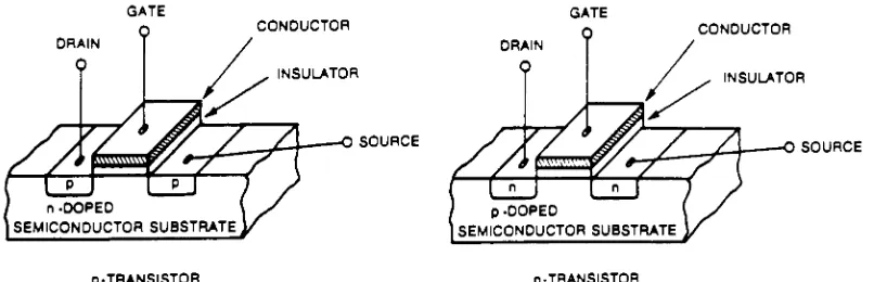
MOSFETs
An
MOS
(Metal-Oxide-Silicon)
structure is createdby
superimposing
severallayers
of conducting,insulating,
and transistorforming
materials (LOCOStechnology).!
5]
nMOStechnology
providestwo types of transistors (or
devices),
an enhancement-mode n-typetransistor and a
depletion
-mode n-type transistor.On
the otherhand,
CMOS
technology
only
uses enhancementtransistors,
one n-type andthe other p-type.
Typical
physical structures of the two types oftransistors are shown in Fig.
2
as follows.Figure
2
-MOSFET Physical Structures
CONDUCTOR
INSULATOR
SOURCE
CONDUCTOR
INSULATOR
SOURCE
p-TRANSISTOR n-TRANSISTOR
MOSFETs (or transistors) have certain I-V characteristics that
[image:33.543.72.475.456.586.2]result
from
the physics of theMOS
system when coupled to thedrain
and source n+
(or
p+) regions.Current
flow
from
drain
to source Iscontrolled
by
the gate-source voltageVGS,
thedrain-source
voltageV^,
and the source-bulk voltage
VSB.[6]
Depending
on the sign of thethreshold voltage
(VTO),
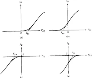
MOS transistors are separated into twocategories.
The
n-type transistors with positiveVTO
are calledenhancement mode
(or
"normally
off")devices,
whereas n-type transistorswith negative
VTO
are said tobe depletion
mode (or"normally
on")devices.
The reverse ofthis situation is the casefor
p-typetransistors.!
7]
This is shown in Fig.
3
for
thefour
types ofdevices
and avery
smallabsolute value ofV^.
Figure
3
-Enhancement
versusDepletion Mode MOSFETs
IDS
vs.VGS
forVSB=0 and very small ABS(VDS). (a) n-type enhancement device; (b) n-type depletion device; (c) p-type enhancement device; (d) p-type depletion device.(< )
A
MOS transistor is termed a majority-carrierdevice,
in which the [image:34.543.131.435.359.617.2]current in a
conducting
channelbetween
the source anddrain
is modulatedby
a voltage applied to the gate.In
the n-typeMOSFET,
themajority
carriers are electrons.A
positive voltage applied on the gatewith respect to the substrate enhances the number of electrons in the
channel
(the
regiondirectly
under the gate oxide) and hence increasesthe
conductivity
of the channel.For
gate voltagesless
thanVTO
thechannel is cut-off, thus
causing
avery low
drain-to-source
current. Theoperation of a p-type
MOSFET
Is analogous, with the exception that themajority
carriers areholes
and the voltages are negative with respect tothe substrate. In the case of
depletion
devices,
increasing
the voltage will reduce the number ofelectrons (orholes)
under the gate oxide andwill
eventually
cause theflow
to cut-off.Several
parameters are used to characterize the operation ofMOSFETs.
Among
them are the threshold voltage,VTO,
thebody
bias,
y.the device
transconductance,
p\ the channellength
modulation,X,
etc.Also,
a set of current-voltage characteristics canbe
extractedby
modeling
the electron inversion (or holeinversion)
layer
created when thegate voltage exceeds (or is
less
than)
VTO- Abrief
discussion
of thesefigures and equations is shown below
for
it isnecessary
tofurther
understand the operation of larger systems, such as the
inverter,
discussed
later on. The approach taken isby
observing
the operation of the n-channel transistor in certain amount ofdetail
and thenextracting
the p-channel
device from
this.Crt-rt
This is the oxide capacitance per unit area.It
is calculatedfrom toX,
as follows:Cox=oX/tox[F/m2],
such that
eox
3.9e0
F/m for
silicondioxide
andE0
=8.854E-12 F/m [2].
VTO:
The
value ofthethreshold
voltage is setby
the electricalproperties ofthe
MOS
system.Internal device
parameterssuch as
doping
densities,
oxidethickness,
and ion implantdose
are establishedduring
the processing, and set thebasic
value this variablewill take. The "O"subscript is
used to
denote
zerobody-bias
(VSB=0). The thresholdvoltage
may
be
calculatedfrom:
^to=
VFB+^+Cox
s(2qeSiNa
^'^[qD^C^rVJ,
where
VFB
is theflatband
voltage,c^
the surface potential,esl=T1.8e0
is the silicon permittivity,Na
is the acceptordoping
concentration in the substrate andDj
is thedose
ofthe threshold adjustment ion implant.
In addition, the absolute value ofthe threshold voltage
decreases with an increase in temperature. Thisvariation
is approximately -4 mV/C
for high
substratedoping
level,
and -2 mV/Cfor low
doping
level.
y: The threshold voltage ofa MOSFET is altered when a source
-bulkvoltage
VSB
is applied. The body-bias (orbody
effect), y,increases
VTn
becauseVSB
adds reverse-biasacross then-channel/p-substrate
boundary
which increasesthebulk
de_
pletion charge. This is
especially
common whenarranging
ofdevices is neededto
form
gating
functions
in series.Applying
body
effectincreases
the third term oftheVTOn
equation toCox1(2qEslNa(<t>s+VSB))i/2.
Thus,
there is aAVTn
increase
givenby
Yn((*5+VSB),/2-(j>s),/2).
Therefore,
VTn=VTOn+
Yn((2-ABS(<t>F)
+ VSB)i/2-^-ABSfojOP'S),
whereYn= Cox1(2qeslNa)^2
ryi/2],
^aABS
is the absolute value ofthe term Inparentheses.!
7),[ 8]
MOSFETs have
three regions of operation: cut-off,linear
and saturation.The terminal
characteristics ofthedevice
are givenby
a plot of!ds
againstVds
for different
values ofVGS.All
voltages are referenced with respect to the source voltage, which is assumed tobe
at ground [image:37.543.169.385.387.584.2]potential in this case. The source and substrate are assumed to
be
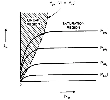
connected together. The characteristic curves are shown in Fig. 4.Figure 4
-I-V Characteristics
for
n-&
p-transistors'V -V,| - iVj gi l at
UJ
M^
These
characteristics, as mentioned earlier, are extractedfrom
the electron (orhole)
inversionlayer
under the gate whichforms
theconduction channel
from drain
to source.Modeling
canbe
performed atvarious
levels
with the generaltradeoff
being
complexity
versus accuracy.The basic
analytic models are obtainedusing
charge control arguments within thegradual-channel
approximation.
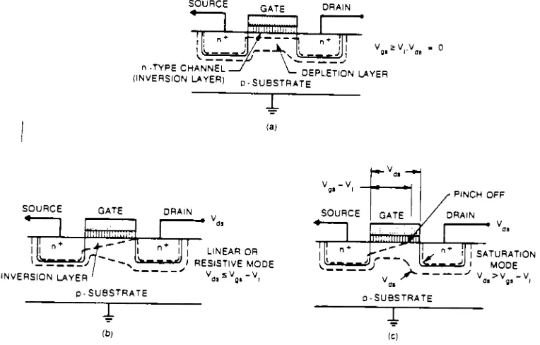
Consider
the crossectionshown in
Figure
5
below.
Figure
5
- nMOSDevice
Conducting
Channel Behavior
SOURCE GATE DRAIN
T
l
^
v 2V,v - o n-TYPECHANNEL, ^
ncp,ftiomiavcd
(INVERSIONLAYER,
.SUBSTRATE
0 "
X
(a)
SOURCE GATE DRAIN
iii^-si'yf-^
iiiin;li!!iiii[
r^*rINVERSION LAYER
I LINEAR OR '^-^> RESISTIVEMODE VSVV. p-SUBSTRATE
T
(b) V -V SOURCE GATE SMnrjg. PINCH OFF DRAIN T I SATURATION I MODE JT~ 'V >V -V at g) I Sa -r~ J
P-SUBSTRATE
I
(C)
To
induce currentflow,
two conditions are necessary.First,
VGS>VTn
is required to create a channel.SecondVos
mustbe
applied toproduce the channel electric
field E.
Thisfield forces
electronsfrom
thesource to the
drain,
thereby
giving
currentflow
ID
In the oppositedirection.
[8]
After a rather complex set ofderivations
andintegrations,
severalvariables ofinterest are obtained.
The
first
ofthese is the processtransconductance
KP
(or process gainfactor),
which equals[inCox
[image:38.543.86.468.217.461.2][A/V2].
The
device
geometry
plays avery
important role, which iscompletely
specifiedby
thedesigner.
This
roleforms
the aspect ratio(W/L),
which in turndetermines
the current.Since
the aspect ratio isset
by
thedevice
layout,
it is the easiest parameter to controlfor
circuitdesign.
From
this set ofvalues, thedevice
transconductance (orp)
canbe
obtainedfrom
the equation /3 =Kp(W/L)
[A/V2],
and is used tocharacterize a specific
device.
From this set of equations and thegradual-channel analysis, the
basic device
equations are obtained asfollows.
There are, as mentioned
before,
several models that can beconsidered.
Among
them are the square-law model, thebulk-charge
model and the simplified
bulk-charge
model. The square-law
modelassumes that
VTn
is a constant in the channel. This model isusually
chosen
for
circuit analysisdue
to thesimplicity
it shows. Since thisapproach ignores some fundamental device physics, errors are
automatically
introduced into the analysis. This should not be aproblem as
long
asonly
general calculations are made with theseequations.
A more accurate equation set is obtained
by
noting
that thechannel voltage V is underneath the oxide and increases the effective
bias
on the MOS system. On the otherhand,
the increasedcomplexity
can offset the desire
for
precision, particularly whenperforming
calculator-based estimates. This is the mam reason the square-law
model is more commonly used
for
manual computations.A
simpler model which retains some of theaccuracy
ofthebulk-charge analysis can
be
obtainedby
performing
aTaylor
series expansionon the voltage terms in the
bulk-charge
equation.[8]
Including
thebody-bias factor
andconsidering
only
first
order terms givesCox
i(2qeslNa(2-ABS(<j>F)+V+VSB))i/2
Yf.2-ABS(4>F)+VSB)i/2-dV,
where d =
y/[2(2-ABS0M+Vsb)1/2]
is the slope.Thus,
with the use of the current integral equation (seedevice
physics
bibliographical
reference) and the above equationsgivesIon
=(Pn/2)!2(VGS
-VTn)VDS
-(1+3)^].
The presence of the
(1+d)
term reduces the current to a morecorrectvalue. The threshold voltage is interpreted as the value needed to
invert the surface at the source end of the channel. The saturation
voltage is given
by VDS
sat =(VGS
-VTn)/(l+d),
which in turn giveIon
=!pV(2(1+3))](Vgs
- VTn)2[l +MV^
- VDS>sat)].The accuracy ofthese analytical models is
limited
by
thefact
thatthe gradual-channel approximation is a 1-dimensional approximation to
the 3-dimensional MOSFET structure. Computer simulations provide
the
key
to understanding the details ofthe transistor operational modes.Now,
the effective channellength
is afactor
to consider whenscaling
ispresent in the design ofstructures
for
VLSI systems. This channellength
can
be
approximatedby:
Leff
=L
-[2E0(ESi/qN)(VDS
-(VGS
- VTn))]/2.This
is a simple
way
to approximate the effects of the channellength
modulation
factor
k,
which is ever present in the current-voltagerelationships in
MOSFETs.
In
the case of pMOStransistors,
the sameequations apply,
only
changing
some signs to makeup
for
thedifferences
in
threshold
voltage effects, as well as other intricacies of thedevice
physics of
holes
asmajority
carriers.Moreover,
therehave
tobe factors
to make
up for
thefact
that thedrift
and maximumvelocity
of thecarriers in n-type
devices
is about2.5
times that of p-typedevices.
Continued discussion
of thedetails
ofMOSFETs
couldlead
to along
discussion
offacts
and equations that arehard
to visualize and toocomplex
for
the scope ofthis thesis.Therefore,
the relevant equations toconsider, as well as others that relate them to others are shown in table
2
asfollows.
It isleft
to the reader tostudy
the theoretical conceptsbehind
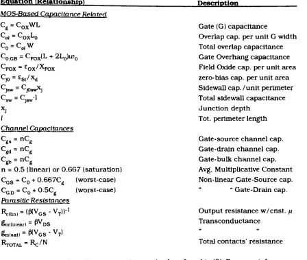
those equations and parameters ofinterest in this table.Table
2
MOSFET
Characteristic Equations
ofRelevance
Equation (Relationship) Description
Threshold VoltaoeRelated
vfb
=*ra-%/Cox)-Cox-l/0*>x(xVxovtoovfxW Flatband Voltage^GS= "^M'
*Slmc"=u g<="-c; W6ik functioniliffcicnCc between Gate & Substrate
<I>ClS
s -(kT/q)ln((NaNd;poly)/
n,2
) (porysilicongate)
kT/q
Thermal Voltageq= 1.602E-19 Coulombs Electronic chargeConstaT
k=6.62E-5eV/"K
4>S
~2-ABS(<ty)
ABS^stkT/qllnfN^n,)
Boltzmann Constant
Surface Potential
Bulk Fermi Potential(p-type)
table
2
(continued)
Equation(Relationship)
MOS-Based Capacitance Related
Cg
=CQXWLS>l =
*-"OX^0
*-"0,GB
=^-TO^L +2L0)UJ0
*-TOX
=OX'*FOX
^p
=S1'"d
^Jsw
=^-JOsw*)
r =c 1/ Channel Capacitances
Cgs
-"Cg
Cgd
=nCg
Cgb
=nCg
n =0.5 (linear)or0.667 (saturation)
Description
-GS
C0
+0.667Cg
:
C0
+0.5Cg
ParasiticResistancesRenin.
=(P(VGS-VT))-1Smlllnear)
= P*DS
gm....)=P(VGs-VT)
Rtotal
=Rc/N(worst-case)
(worst-case)
Gate (G)capacitance
Overlap
cap. per unitGwidthTotal overlapcapacitance
Gate
Overhang
capacitanceField Oxidecap.per unitarea
zero-biascap. perunitarea
Sidewallcap./unitperimeter Totalsidewallcapacitance
Junction depth Tot.perimeterlength
Gate-source channelcap.
Gate-drainchannel cap.
Gate-bulkchannel cap.
Avg. MultiplicativeConstant Non-linearGate-Sourcecap.
"
Gate-Draincap.
Outputresistancew/cnst.n
Transconductance
Totalcontacts' resistance
Note: Thistable isbased upon equations and values foundin[8]. Formore info., please readDevice PhysicsandVLSIDesign
theory
bibliographicalreferences.2.2.2
InvertersThe simplest, and yet most fundamental
logic
structurebeyond
that of the MOSFET is the inverter. The reasonfor
this is thatany
structure, whether nMOS, pMOS or CMOS can
be
reduced to an inverterequivalent which can
hold
thetiming,
capacitance and resistancecharacteristics of the larger structure. There exist two main types of
[image:42.543.54.502.79.458.2]MOS
inverters which arebeing
used today.These
are: the nMOS inverterconsisting
of two nMOStransistors,
onedepletion
mode and oneenhancement mode; and the
CMOS
inverterconsisting
of twoenhancement
devices,
one nMOS and one pMOS. In order to understandthe
function
and electricaldifferences
between
these twokinds
ofinverters,
adiscussion
follows for
each ofthem.2.2.2. J
The nMOSInverter
It consists of a "load" resistance R called the
pull-up
resistor, anda pull-down transistor
T
connected in seriesbetween supply
voltageVdd
and ground GND. The resistor is sized to
limit
thepull-up
current tosome
fraction
of maximum pull-down current providedby
thetransistor.!9]
This is shown in Fig.6 below.
Figure
6
- nMOSInverter Basic Structure
v'
O-Vdd
I
17
1
Gnd
f
t
Gnd(a)
-oV0
-" y
K
Gna
(b)
As
canbe
seen above, the inputvoltageVln
is applied to the gate ofT,
which provides avery high
input impedance via the gate capacitanceC
This,
in turn, will drive a similar output capacitanceC.
If
Vln
isless
[image:43.543.113.457.381.561.2]than the
threshold
voltage ofT,
theload
capacitanceC
willbe
charged toVdd.
Although
Vwt
will neverbe
equal toVdd
due
to a small leakagecurrent
flowing
through
T,
but
it will approach it.If
Vin
israised beyondthreshold,
T willinitially
conduct in saturation,C
will startdischarging
(pulling
down
V^)
and1^
will increasedue
to thelarge
value ofVgs
(Vln)
until T moves into the
linear
region of operation.When
Vin=Vdd
theoutput voltage will
be
givenby
V^R^/tR^+R)),
such thatR^
is thechannel resistance at this point and R is the resistance
due
to thepull-up
resistor. In order tohave
Vout
less
than threshold Rs4Rch
must hold.In orderto
be
able toachievehigh
speeds ofoperation, the value ofR must
be very
small,but
not smaller than 4 Rch. There are twoways toachieve this. The
first
isusing
an integrated circuit resistor, which takestoo much silicon area. The other is
by
using
adepletion
mode transistoras
pull-up load
(shown in Fig. 6b).Having
this particular structure,after some mathematical
derivations,
yields the pull-down &pull-up
equations and characteristics shown below.
Table 3
nMOS Inverter Characteristic Equations
Pull-downCurrentEquations
Ipd
=0 whenVin-Vth
< 0 (off)1^
=(6d/2KVln-Vthr2
when 0s
Vln-Vth
sVQut
(saturation)1^
=6d(Vln-Vth
-0.5Vout)Vout whenVin-Vth
>VQut
(linear) suchthat6d
=(^E/TpxXW/L)Pull-up
Current Equations (DepletionTalways conductssinceV^-V^
>0holds)
IpU
=0.56u(ABS(Vdep))2
when ABS(Vdep)s Vdd-
VQut
(saturation)Ipu
= 6U[(ABS(Vdep))-0.5(Vdd-Vout)](Vdd-VQut). ABS(Vdep) >Vdd-VQut
(linear) such that6U
= (/<e/ToxMW/L)Superimposing
theoperating
curves ofboth transistors,
we obtainthe characteristic curves
for
the nMOSinverter.
This
is possible since1^
flows
inboth pull-up
and pull-downtransistors.
Thus,
the voltagetransfer
curve is as shown inFig. 7b
below
along
with theIds
versusVcurve (Fig. 7a).
[image:45.543.97.473.205.420.2]out
Figure 7
- nMOSInverter
Characteristic
Curves
(a)
(b)
Point A
in these curves above corresponds to pull-down off,pull-up