This is a repository copy of
Responsivity of quantum well infrared photodetectors at
terahertz detection wavelengths
.
White Rose Research Online URL for this paper:
http://eprints.whiterose.ac.uk/1685/
Article:
Gadir, M.A., Harrison, P. and Soref, R.A. (2002) Responsivity of quantum well infrared
photodetectors at terahertz detection wavelengths. Journal of Applied Physics, 91 (9). pp.
5820-5825. ISSN 1089-7550
https://doi.org/10.1063/1.1467951
eprints@whiterose.ac.uk https://eprints.whiterose.ac.uk/
Reuse
See Attached
Takedown
If you consider content in White Rose Research Online to be in breach of UK law, please notify us by
derived. The model examines the responsivity, carrier capture probability and quantum efficiency. It is found that the QWIP sensitivity reaches a plateau below the 10 mm detection wavelength and remains nearly constant from 10 to 50mm. © 2002 American Institute of Physics.
@DOI: 10.1063/1.1467951#
I. INTRODUCTION
Quantum well infrared photodetectors~QWIPs!have at-tracted the attention of many researchers during the last decade,1– 4and the detailed physical understanding of QWIP operation has stimulated study of optimum QWIP design. This has resulted in the proposal of several theoretical models5– 8to express primary QWIP characteristics such as responsivity, detectivity, photoconductive gain and photocur-rent. However, the QWIP formulas derived from these dif-ferent models vary due to the diversity in definitions and basic assumptions.
In this article, a simplified unifying model is presented with the aid of some of the definitions and assumptions from the models mentioned before. It starts by defining the photo-current in a simple detector and linking the physical charac-teristics of capture probability, gain, and ultimately the re-sponsivity, to the detection wavelength. The aim is to understand the consequences on the photocurrent of extend-ing the detection wavelength of QWIPs to their far-infrared or terahertz limits.
II. PHOTOCURRENT AND PHOTOCONDUCTIVE GAIN
Figure 1 shows a simple schematic diagram of a detector,9where L is the thickness and Ad is the surface area
of a slab of photoconductive material, andFs is the optical
flux incident normally. The intensity of the flux is usually taken to decrease exponentially with the penetrating depth z,9 hence, the intensity of flux at any depth z is
F~z!5Fs~12r!exp~2az!,
where r is the reflection coefficient of the surface andais the absorption coefficient of the material.
The photocarrier generation rate per unit volume is given by9
G~z!52
1
Ad
dF~z!
dz ,
[G~z!5
a
AdFs~12r!exp~2az!.
At steady state the photogenerated carrier density P(z) is constant i.e.,
]P~z! ]t 50,
hence, the generation rate must be equal to the recombina-tion rate. Say the latter is described by a recombinarecombina-tion life-timet, then
]P~z!
]t 5G~z!2 P~z!
t 50,
and hence
P~z!5tG~z!.
The average photoelectron density is therefore
P ¯51
L
E
0L
2P~z!dz5
1
L
E
0L
G~z!tdz
5aFst
LAd~12r!
E
0L
exp~2az!dz,
[P¯5 Fst
LAd
~12r!@12exp~2aL!#5hFst
LAd
,
whereh is known as the quantum efficiency and is defined here as the probability that a photon is absorbed in a quan-tum well to produce a photoexcited electron. This quanquan-tum well efficiency is shown later
h5~12r!@12exp~2alw!#, ~1!
where the absorbing length L is now taken as the width lwof
the quantum well.10Thus,alw. Recalling that a general
cur-rent density is of the form ‘‘nev,’’ then the photocurcur-rent
Ip5P¯ evAd⇒Ip5~hFs!e
tv
L ,
a!Electronic mail: eenmag@leeds.ac.uk
5820
thus
Ip5eFshg, ~2!
where g is known as the photocurrent gain and can be inter-preted as the ratio of the electron mean free path tv to the
sample thickness L and is interpreted as a measure of the photoelectron transport.9,11 The photoconductive gain is viewed in terms of a quantum well capture probability Pc
and is derived from Fig. 2, see Refs. 7 and 10.
The total photocurrent consists of the remaining photo-current ~i.e., electrons not captured by the well! (12Pc)Ip
and the emitted current from the well (12Pc)ip,
10
see Fig. 2. In order to maintain current continuity
Ip5~12Pc!Ip1~12Pc!ip,
[IpPc5~12Pc!ip
after using the definition in Eq. ~2!, Ip and ip become
10
Ip5eFshng and ip5eFsh,
wherehnis the quantum efficiency of a number N of wells in
a QWIP, and h is the quantum efficiency of a single well with unit gain. Now PcIp5(12Pc)ip, therefore
eFshng Pc5~12Pc!eFsh,
[g5 12Pc
Pc
h hn
.
Recalling thathn5hN, then
g512Pc
Pc
1
N ~3!
as deduced by Levine et al.,7,10
III. RESPONSIVITY
The responsivity of a QWIP is a commonly used figure-of-merit for detector performance and is defined as the pho-tocurrent per unit watt of incident light,9 i.e.,
R5
ehg
hn , ~4!
now
n5cl,
thus, in terms of wavelengthl:
R5ehg
hc l. ~5!
Taking the photoconductive gain g from Eq.~3!, then
R5
eh
hcl 12Pc
Pc
1
N. ~6!
Using this expression, Fig. 3 illustrates the responsivity R as a function of detection wavelength l, for various, but fixed, capture probabilities Pc. It can be seen that there is a
direct proportionality between R andl. The standard capture probability Pc of 0.346 was taken from the 5 mm
Si0.64Ge0.36/Si QWIP of Ref. 12, and the absolute values of
the responsivity were calculated assuming a constant quan-tum efficiency h of 10% which is typical of many n- and p-type devices.7,12,13The number of wells in Fig. 3 was fixed at N510.
[image:3.612.321.552.50.212.2]IV. CAPTURE PROBABILITY
[image:3.612.72.266.51.187.2]Figure 4 shows the results of calculations14of the detec-tion wavelength l versus the quantum well width lw for a
FIG. 1. The geometry of a detector.
[image:3.612.57.268.510.723.2]FIG. 2. Schematic band diagram of a unit gain single well in a QWIP including the total net photocurrent Ip and the emitted photocurrent by a single well.
FIG. 3. Responsivity vs detection wavelength for a range of capture prob-abilities Pcthat are independent ofl. The reference value for Pcof 0.346 was taken from Ref. 12.
[image:3.612.79.268.607.719.2]series of Si12xGex/Si quantum wells. The solid lines show
curves fitted via A and B to the data of the form
l5 A
lwB. ~7!
It was found that the exponent B was always very close to 1, thus for the purpose of this work
l5lA w
~8!
with the parameter A ~having the dimensions of cm2! de-pending on the depth~in this case, the Ge concentration x!of the well. The Si0.64Ge0.36/Si QWIP12mentioned earlier, is to be used as an example device configuration. For this material concentration, it was found that the constant A linking the wavelengthland the quantum well width lw @as in Eq.~8!#
was 2.248310210 cm2. The GaAs/Ga
0.74Al0.26As material
system employed in the QWIPs of Ref. 15 will also be used. In this case A was found to be 4.83310210cm2.
In the previous section the capture probability was as-sumed to have no dependence on l, however, it would be expected in practice that the capture probability increases with increasing well width, as illustrated with the aid of the arrow thickness in each well in Fig. 5. There are two
impor-tant limits
Pc→0 as lw→0
and
Pc→1 as lw→`.
Both of these limits could be fitted empirically by taking the capture probability as
Pc512exp
S
2lwLc
D
, ~9!where Lcis a decay constant defining the rate of increase of
the capture probability Pc with well width lw. Using the
expression for the wavelength dependence on the well width @Eq. ~8!#, then the capture probability can be expressed in terms ofl, i.e.,
Pc512exp
S
2A LclD
. ~10!
Now substituting Eq.~10! into Eq.~6!gives a relation-ship between the responsivity and the detection wavelength which includes this simple model for the capture probability. Thus, the responsivity becomes
R5 eh
hcNl
exp
S
2A LclD
12exp
S
2A LclD
. ~11!
With the aid of Eq.~11!, Fig. 6 replots the data of Fig. 3 ~with the capture probability Pc scaled so that Pc50.346
whenl55mm!to display R as a function oflfor several of the lengths Lc. It can be seen that the responsivity increases
[image:4.612.316.558.51.220.2]superlinearily with detection wavelength. This is because un-der this model the capture probability decreases with increas-ing wavelength, thus increasincreas-ing the photoconductive gain g.
[image:4.612.57.293.52.232.2]FIG. 4. Detection wavelengthlvs well width lwfor different Ge concen-tration with fitted curves.
FIG. 5. Schematic illustration of the proportion of the photocurrent which is captured by subsequent quantum wells.
[image:4.612.98.260.605.732.2]V. QUANTUM EFFICIENCY
To improve the model still further, focus is now redi-rected towards the well quantum efficiencyhwhich has been taken as constant. In Ref. 11, this quantum efficiency is de-fined as
h5P~12r!@12exp~2Balw!#, ~12!
where P is a polarization dependent constant ~P51 for p-type QWIPs!, a is the absorption coefficient and B is a constant depending on the number of paths the infrared ra-diation made through the QWIP active region. In the worst case of a semiconductor/air reflection coefficient r51/3 and B51, the quantum efficiencyhwould become
h523@12exp~2aNlw!#, ~13!
where, in an N well device, Nlwis the total width of absorb-ing material. Usabsorb-ing the relationship between the well width and the detection wavelength given in Eq.~8!, we get
h52
3
S
12expF
2aN Al
GD
. ~14!The absorption coefficient a depends on the material system and the doping density. From Ref. 12, we obtain a
536.153103 cm21 for those particular 10 Si0.64Ge0.36/Si
quantum wells which are homogeneously doped with boron giving a sheet concentration of ps51.231012 cm22.
Whereas, from Ref. 15a525.43103 cm21for the 25 period
GaAs/Al0.26Ga0.74As QWIP with a doping density ND51.4
31018cm23 and surface grating to allow normal incidence.
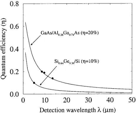
Then, substituting these values into Eq.~14!, we obtain theh
curves shown in Fig. 7. Then, returning to Eq. ~11!we cal-culated the effect of the wavelength dependent quantum ef-ficiency h summarized in Eq. ~14! upon the responsivity-versus-wavelength relationship, but this time reverting back to the case of constant capture probability~see Fig. 8!. The model assumes that the peak absorption coefficient is con-stant for all devices made from the same material, regardless of their absorption wavelength. In fact, the absorption
coef-ficient depends on the doping density, so for a constant dop-ing density within the quantum wells, the absorption coeffi-cient would become a function of the well width lw and,
hence, it would also be a function of the detection wave-lengthl. For generality and to remove an additional variable from the analysis, the assumption is made that a series of devices could be designed to have the same absorption coef-ficient. This would be achieved by increasing the doping density as the width of the quantum wells is decreased—in order to achieve the same sheet density of carriers.
VI. COMPLETE MODEL
[image:5.612.320.552.47.238.2]Figure 9 shows the behavior of the responsivity when both the capture probability and the quantum efficiency are allowed to be functions of the detection wavelength. We sub-stituted Eq. ~14! into Eq. ~11! as shown in Eq. ~15!, thus completing the model
FIG. 7. Quantum efficiency as a function of detection wavelength for the example material systems~see Refs. 12 and 15!.
[image:5.612.59.290.51.243.2]FIG. 8. Responsivity as a function of detection wavelength for a constant capture probability and a variable quantum efficiency in SiGe/Si and GaAs/ AlGaAs quantum wells. Lc5150 Å.
FIG. 9. Responsivity as a function of detection wavelength for a variable capture probability and quantum efficiency~as a function of detection wave-length!. Lc5150 Å.
[image:5.612.322.554.538.722.2]R5hcNe l
exp
S
2A LclD
12exp
S
2A LclD
2
3
S
12expF
2aN Al
GD
. ~15!In Fig. 9 we took A52.248310210cm2 and N
510 as for the SiGe devices of Ref. 12 and A54.83310210cm2
and N525 as for the GaAs/AlGaAs devices of Ref. 15. It can be seen that there is almost a direct proportionality, mir-roring the simple constants-based model at the beginning of this work. However, the absolute magnitudes of the respon-sivity are now more justified. Further consideration needs to be given to this data because although the responsivity in-creases with detection wavelength, it does not tell the full story. The unit of the responsivity is milliamps per watt with the latter representing the incident power. As the detection wavelength increases the photon energy decreases, hence, there are more photons per watt, which may be expected to produce more photoelectrons and thus more photocurrent.
In effect
R5Ip
P,
where Ip is defined in Eq.~2!and the incident power is
P5Nphn5Np
hc l .
Np is the number of photons per second. Hence, the
com-plete photocurrent Ip equation becomes
Ip5R P5Np
e
N
exp
S
2A LclD
12expS
2ALcl
D
2
3
S
12expF
2aN A lGD
. [image:6.612.326.546.49.228.2]~16!
Figure 10 shows the photocurrent per incident photon (Np51) as expressed in Eq.~16!.
This is perhaps more vividly illustrated in Fig. 11 where
the current is now given in terms of the number of photoex-cited electrons per second
Number of photoexcited electrons51.6 Ip 310219C.
~17!
Both figures show that in these terms the sensitivity of the QWIPs reaches a plateau and for increasing wavelength a constant number of electrons can be expected to be photoex-cited per incident photon. ~It maybe disconcerting to see SiGe QWIPs with 10% quantum efficiency having higher responsivity than 20% efficient GaAs/AlGaAs QWIPs. No significance should be attached to this, because the devices have different numbers of quantum wells and different dop-ing densities, etc.!
VII. CONCLUSION
This article has derived two essential relationships for the capture probability and the quantum efficiency, each one as a function of the detection wavelength. These dependen-cies have enabled the responsivity to be expressed in terms of the detection wavelength. Subsequently, a photocurrent model was established by focusing on the remaining factor: the incident power ~i.e., P5Ip/R!. As the latter was
re-stricted to the power of a single photon, then the number of photoexcited electrons~to produce the photocurrent!was de-termined. It was found that the number of photoelectrons per incident photon is likely to tend towards a constant as the wavelength of the incident light is increased beyond 10 mm and into the terahertz region of the spectrum. This is an encouraging result and suggests that far-infrared QWIPs may have a sensitivity no less than those in the midinfrared re-gion. The realization of such devices will therefore be depen-dent upon the dark current in order to obtain a viable signal-to-noise ratio.14,16 –19
1S. D. Gunapala et al., SPIE Conference on Infrared Detectors and Focal
Plane Arrays V, April 1998, p. 3379.
2S. Gunapala, G. Sarusi, J. Park, T. L. Lin, and B. Levine, Phys. World 7,
35~1994!.
[image:6.612.54.288.51.244.2]FIG. 10. Photocurrent as a function of detection wavelength when the power is 1 photon per second. Np51.
[image:6.612.70.296.298.352.2]3P. Kruck, A. Weichselbaum, M. Helm, T. Fromherz, and G. Bauer,
Super-lattices Microstruct. 23, 61~1998!.
4D. J. Robbins, M. B. Stanaway, W. Y. Leong, J. L. Glasper, and C.
Pick-ering, J. Mater. Sci.: Mater. Electron. 6, 363~1995!.
5B. F. Levine, Semicond. Sci. Technol. 8, S400~1993!. 6
C. H. Liu, Appl. Phys. Lett. 60, 1507~1992!.
7
B. F. Levine, J. Appl. Phys. 74, R1~1993!.
8M. Ershov and H. C. Liu, J. Appl. Phys. 86, 6580~1999!.
9K. K. Choi, The Physics of Quantum Well Infrared Photodetectors~World
Scientific, Singapore, 1997!.
10
B. F. Levine, A. Zussman, S. D. Gunapala, M. T. Asom, J. M. Kuo, and W. S. Hobson, J. Appl. Phys. 72, 4429~1992!.
11Handbook of Nanostructure Materials and Nanotechnology; Optical
Properties, edited by H. S. Nalwa~Academic, New York, 2000!, Vol. 4.
12T. Fromherz, P. Kruck, M. Helm, G. Bauer, J. F. Nutzel, and G. Abstreiter,
Appl. Phys. Lett. 69, 3372~1996!.
13R. People, J. C. Bean, G. C. Bethea, S. K. Sputz, and L. J. Peticolas, Appl.
Phys. Lett. 61, 1122~1992!.
14M. A. Gadir, P. Harrison, and R. A. Soref, Superlattices Microstruct.
Su-perlattices Microstruct. 30, 135~2001!.
15
Intersubband Transitions in Quantum Wells: Physics and Device Applica-tion 1; Semiconductors and Semimetals, edited by H. C. Liu and F. Ca-passo~Academic New York, 2000!, Vol. 62.
16N. E. I. Etteh and P. Harrison, IEEE J. Quantum Electron. 37, 672
~2001!.
17
N. E. I. Etteh and P. Harrison, J. Appl. Phys.~accepted for publication!.
18N. E. I. Etteh and P. Harrison, Physica E~Amsterdam! ~submitted!. 19M. A. Gadir, P. Harrison, and R. A. Soref, Physica E~Amsterdam! ~
sub-mitted!.