100 Gbit/s COMPUTER OPTICAL INTERCONNECT
Ivan Glesk½
, Robert J. Runser, Kung-Li Deng, and Paul R. Prucnal Department of Electrical Engineering, Princeton University, Princeton, NJ08544
Received 23 September 1999, accepted 16 November 1999
An experimental demonstration of an error free 100Gbit/s optical time division multiplexing (OTDM) broadcast star computer interconnect is presented. A highly scalable novel node design provides rapid inter-channel switching capability on the order of the single channel bit period (1.6 ns).
PACS:42.79.Sz, 42.79.Ta
1 Introduction
Although lightwave technology is meeting the demand for point-to-point and long-haul transport of digital information, routing packets at the nodes of the network has typically been carried out using electronically switched backplane routers. The growing capacity on the Internet is plac-ing an ever greater demand on electronic routplac-ing technologies. While WDM can support large aggregate traffic bandwidths, it is difficult to perform routing functions which may involve chal-lenging techniques such as dense wavelength conversion. Additionally, present WDM laser and filter tuning techniques rely upon slow technologies which increase the channel access latency and reduce the effective network bandwidth.
Recent advances in optical time division multiplexing (OTDM) have proven this technolo-gys capability to handle the switching and routing needs for future. Channel access in OTDM networks is achieved by using time slot tuners and all-optical demultiplexers. Timing precision of less than 1ps is required to tune, multiplex, and demultiplex individual channels within the OTDM frame.
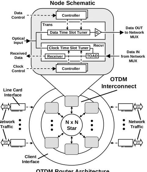
The computer interconnect we are constructing is based upon an OTDM broadcast star ar-chitecture. The high-level architecture and node design is shown in Fig. 1. Nodes transmit information at a slow data rate, , by modulating picosecond optical pulses. By using a scalable time slot tuner, the pulse is appropriately delayed to correspond to the desired destination time slot. Data pulses from all nodes are multiplexed into a time frame with an aggregate bandwidth of , where is the number of nodes in the network. The pulse spacing between adjacent
channels is
½
or typically less than 10ps to achieve 100+ Gbit/s. Ultrafast all-optical de-multiplexers like the TOAD are used to extract the desired channel from the high capacity OTDM
½
E-mail address: [email protected]
Optical Input Trans Recvr Data OUT to Network MUX
•
•
•
•
•
•
N x N Star Client Interface OTDM Interconnect Controller G Receiver Clock Control Received Data TOAD
Clock Time Slot Tuner
OTDM Router Architecture
Line Card Interface Network Traffic
•
•
•
I/O I/OData Time Slot Tuner
[image:2.612.194.435.38.320.2]Data IN from Network MUX Network Traffic
•
•
•
I/O I/OFig. 1. OTDM network and node architecture
frame at the node receivers. Nodes can select the received time slot by using a time slot tuner to align the clock with an incoming time slot within the frame for all-optical demultiplexing.
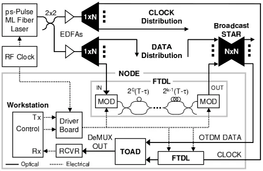
Fig. 2. Experimental OTDM computer interconnect and node architecture
2 Experimental Demonstration and Results
Fig. 2 shows the network and novel node architecture experimental setup. The two key optical components of the node are the recently developed fast tunable delay line (FTDL) [5] and the ter-ahertz optical asymmetric demultiplexer (TOAD) [6]. A controller card residing in a workstation sends electronic NRZ data at the single channel bit rate, B, and control bits to the driver board specially designed to control the two FTDLs on the clock and data fibers. The FTDLs consist of cascaded feed-forward Mach-Zehnder fiber delay lattices designed to produce optical copies of the incoming pulse stream organized into -bit subcells spaced by with inter- subcell bit
spacing [5]. The two modulators controlled by the driver board select one of the
time slots into which one of the copies is transmitted. The FTDLs in the node are used to transmit data into a selected time slot within the OTDM frame and align the clock with a given time slot for optical demultiplexing. Ultimately, the dimensionality of the network,, is determined by , the number of stages in the FTDL. The intermediate processing bandwidth,
¼
, of
the driver controller and the electro-optic modulators is designed to match the repetition rate of the picosecond pulsed fiber laser source and is related to the single channel bit rate as ¼
.
Pulses are amplified by EDFAs and distributed to the individual nodes by splitters. After
node data modulation and time slot selection, the data is multiplexed by precision fiber delays feeding an NxN star coupler. The high bandwidth OTDM frame is broadcast to all nodes in the network. Each node can demultiplex any single channel from the frame using an FTDL on the clock and a TOAD.
In our experimental testbed, we populated 16 time slots in the OTDM frame by
constructing 2 stage FTDLs. The single channel data rate was chosen to match the OC-12
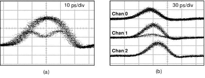
Fig. 3. 100 Gbit/s multiplexed data OTDM subcell eye diagram on bandwidth limited detector, and demul-tiplexed TOAD output eye diagrams for three channels in subcell. (a) 100 Gbit/s muldemul-tiplexed data ODTM subcell eye diagram (b) Demultiplexed TOADF output eye diagrams.
electronic processing bandwidth were set to the OC-48 rate ( ¼
2.48832 GHz). The
simple electronic design of the driver board permits the rapid control of the FTDL and provides low latency, arbitrary channel selection. The driver board was constructed using 4-bit electronic multiplexers (Vitesse) and simple logic operating at the OC-48 rate. To produce an OTDM frame with an aggregate bit rate of 100 Gbit/s, = 10 ps was chosen. Each TOAD was designed with
a demultiplexing window width of about 10 ps at FWHM and a polarization splitter was used to separate data from clock at the output.
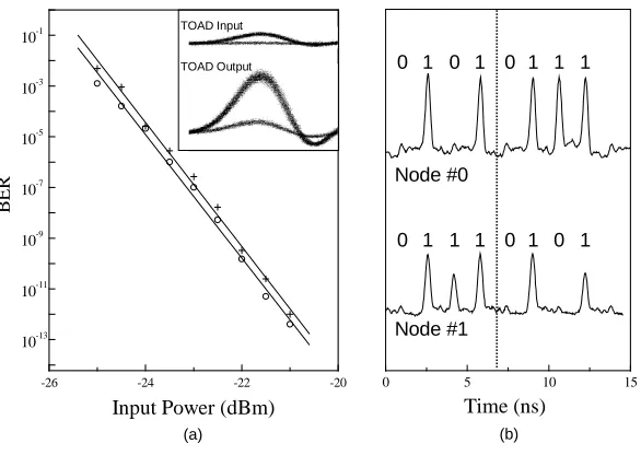
The 100-Gbit/s multiplexing and demultiplexing experimental results are shown in Fig. 3. According to the design of the FTDL, the 16 time slots in our OTDM frame are arranged in 4 subcells each containing 4 time slots spaced by 10 ps. Our network demonstration focused on one of the subcells within the frame. Fig. 3a shows the aggregate eye diagram for a subcell with multiplexed data from 4 nodes with a fixed pattern, 1 -pseudorandom- 1 - 0, on a bandwidth limited detector (34-GHz photodetector, 50-GHz oscilloscope). Upon demultiplexing by TOADs tuned to the individual channels, each is resolved in Fig. 3b (the 4th time slot is omitted as it is 0).
-26 -24 -22 -20
10-13 10-11 10-9 10-7 10-5 10-3 10-1
chan 0 chan 1
BE
R
Input power (dBm)
Input Power (dBm)
(a)
TOAD Input
TOAD Output
(b)
0 5 10 15
time (ns) Node #0
Node #1
0 1 0 1 0 1 1 1
0 1 1 1 0 1 0 1
[image:5.612.162.455.49.257.2]Time (ns)
Fig. 4. BER of channels 0 and 1 against average single channel input power, and demonstration of rapid channel selection on bandwidth limited analogou detector. (a) BER of channels 0 and 1 against average single channel input power. Inset: TOAD input and output eye diagrams demonstrating gain.Æ- channel 0, + - channel 1. (b) Demonstration of rapid channel selection.
trace) of a TOAD demultiplexing a single channel of pseudorandom data with identical oscillo-scope settings. The demultiplexed output is larger in amplitude than the input by approximately 6 dB.
switching among data channels with reliable, error free operation and low latency. Since the ac-tive components of the FTDLs do not scale with the number of nodes [5], simply adding another stage,, (3 dB additional loss per node), scales the interconnect up to 64 nodes
with-out taxing the power budget significantly. If OC-24 ( = 1.24416 GHz) is chosen as the single channel data rate and 10-GHz
¼
intermediate processing bandwidth electronics are used, an
80-Gbit/s interconnect with a rapid inter-channel switching speed of 800 ps is feasible. In such a 64-processor architecture, coherent crosstalk does not limit the BER performance significantly [7]. Since the demultiplexer [8] and other optical components in the node can be integrated, we believe this network is practical for future, high-speed multiprocessor interconnect systems.
Acknowledgement This work has been supported by DARPA Contract No. F30602-97-2-0316.
References
[1] R.A. Barry, V.W.S. Chan, K.L. Hall, E.S. Kintzer, J.D. Moores,et al.: IEEE J. Sel. Areas Commun. 14 (1996) 999
[2] J.K. Lucek, P. Gunning, D.G. Moodie, K. Smith, D. Pitcher:Electron. Lett 33 (1997) 887
[3] M. Tsukada, W. De zhong, T. Matsunaga, A. Masaki, T. Oohara: J. Lightwave Technol 14 (1996) 1979
[4] A.G. Nowatzyk P.R. Prucnal: Proc. 22nd Int. Symp. On Computer Arch., Santa Margherita, Italy (1995)
[5] K.-L. Deng, K.I. Kang, I. Glesk, P.R. Prucnal:IEEE Photon. Technol. Lett. 9 (1997) 1496 [6] I. Glesk, J. P. Sokoloff, P. R. Prucnal:Electron. Lett. 30 (1994) 339