Thesis by
Yulia Tolstova
In Partial Fulfillment of the Requirements for the Degree of
Doctor of Philosophy
California Institute of Technology
Pasadena, California 2016
All Rights Reserved
This thesis would not have been possible without the contributions of many, many people.
First, I would like to thank my adviser, Harry Atwater, for being so incred-ibly inspiring and supportive for all these years. There were so many times when I went into Harry’s office feeling defeated and walked out actually want-ing to get back to work. I am also grateful for havwant-ing the freedom to explore and make (so many) mistakes.
I would like to thank my thesis committee — Professors Bill Johnson, Julia Greer, and Austin Minnich — for their helpful feedback and taking the time to review my thesis.
My research experience would not have been the same without mentorship from several people. Ali Ghaffari has been an incredible source of support, vacuum system knowledge, and optimism. I want to thank Carol Garland for her mentorship at the TEM and also giving me the opportunity to help teach the TEM lab. I learned so much from this experience (including the best recipe for brownies).
There are many people at Caltech whose assistance is essential to the suc-cess of many research projects: Mike Roy (CCE Instrument shop), Rick Ger-hart (Glass shop), Rick Germond (Facilities stockroom), Joe Haggerty and Ali Kiani (GALCIT shop), Mike Walsh (Biology electronics shop), Chi Ma (GPS SEM facility), Nils Asplund (KNI), Bruce Brunschwig, and all the GLAs at the MMRC.
I would like to thank all the members of the Earth Abundant semiconduc-tor project with whom I’ve had the privilege of working: Samantha Wilson, Amanda Shing, Greg Kimball, Davis Darvish, Chengxiang Xiang, Naomi Coro-nel, Jeff Bosco, and Faisal Tajdar. It was great to collaborate with several sci-entists from Dow, including Rebekah Feist, Robert Wright, Melissa Mushrush, Manish Sharma, Jim Stevens, Pete Nickias, and Steve Rozeveld. I would also
like to acknowledge my WAVE student Raymond Blackwell. I would like to es-pecially thank Stefan Omelchenko for collaboration and friendship and sharing pots of tea during the last several years.
Many other members of the Atwater, Lewis, and other groups have been incredibly helpful throughout the years. Chris Chen, Hal Emmer, Rebecca Saive, Sunita Darbe, Jung-Shun Huang, Ron Grimm, Nick Strandwitz, Seok-min Jeon, Ragip Pala, Victor Brar, Woochul Jung, Anna Beck, Kate Foun-taine, Ana Brown, Carissa Eisler, Cris Flowers, John Lloyd, Dagny Fleishman, Michelle Sherrott, Krishnan Thyagarajan, and so many others. Thank you all for making my time at Caltech what it was. I would also like to acknowledge the denizens of Watson 250, it was a pleasure to share an office with you guys: Seyoon Kim, Colton Bukowsky, Nick Batara, Muhammad Alam (thank you for providing a broader perspective on life after grad school and lots of useful advice). My daily experiences would not have been the same without the help of Tiffany Kimoto, Jennifer Blankenship, Christy Jenstad, Lyra Haas, Ma-bel Chik, Michelle Aldecua, Connie Rodriguez, Liz Jennings, and Lyann Lau. Your support has made all our lives easier.
Lastly, I would like to thank my family and friends for their support, es-pecially: Amanda “Woman” McNally and my second family (Roberta, Mike, Frank, Nick) — thank you for being there for me all these years; Jennifer Buz, I’m lucky to have had you by my side through high school, college, and grad school; Yinglu Tang, for somehow surviving as my roommate for 4 years and cooking delicious food together. I am most indebted to my mother, Irena Tolstova, for making so many sacrifices to make my life easier, and my grand-father, Nikolai Ostapenko, for taking care of me even from far away. And lastly I want to thank my partner Eliot Hijano for being patient and support-ive during the best and worst of times.
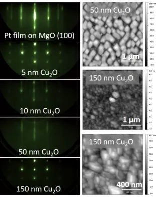
Cuprous oxide (Cu2O) is an earth abundant semiconductor that has several
promising photovoltaic properties, including high absorption in the visible range, high minority carrier diffusion length, and high majority carrier mo-bility. Cu2O can be easily synthesized by oxidation of copper foils in air. One
important advantage that makes Cu2O highly relevant to today’s solar cell
markets dominated by crystalline silicon is its wide bandgap of 1.9 eV at room temperature, which makes it an ideal candidate for a top cell in tandem with a crystalline silicon bottom cell. The detailed balance efficiency of such a device exceeds 44%.
In this work we aim to address several issues that have limited Cu2O solar
cell efficiency. We address the intrinsic p-type nature and chemical instabil-ity of Cu2O by pairing it with an appropriate n-type heterojunction partner
Zn(O,S), which allows us to achieve devices with open circuit voltages exceed-ing 1 V. We identify presence of a current blockexceed-ing layer and reduce it, which results in more than doubling the short circuit current to exceed 5 mA/cm2. Light beam induced current measurements shed light on some of the issues in-herent to polycrystalline Cu2O solar cells, including grain dependent collection
and current losses due to presence of grain boundaries.
In order to address the issues affecting Cu2O made by thermal oxidation we
also develop thin film growth of Cu2O by molecular beam epitaxy on several
substrates including MgO and heteroepitaxial noble metal templates that act as ohmic back contacts. These studies culminate in achievement of the first Cu2O/Zn(O,S) solar cells incorporating an absorber layer grown by molecular
beam epitaxy.
Acknowledgements iii
Abstract v
List of Figures viii
List of Tables xi
List of Publications xiii
1 Introduction 1
1.1 Basics of photovoltaics . . . 1
1.2 Motivation for Cu2O photovoltaics . . . 3
1.3 Energy band alignment . . . 4
1.4 Scope of this thesis . . . 6
2 Molecular Beam Epitaxy of Cu2O Thin Films on MgO 8 2.1 Introduction to Molecular Beam Epitaxy . . . 8
2.1.1 Reflection high energy electron diffraction . . . 9
2.1.2 Thin film growth modes . . . 11
2.2 Growth of Cu2O on MgO . . . 13
2.2.1 Experimental Setup . . . 13
2.2.2 Growth using pure oxygen plasma . . . 15
2.2.3 Growth using 90%Ar/10%O2 plasma . . . 18
3 Heteroepitaxial Ohmic Templates for Cu2O Growth 22 3.1 Metal Films on Dielectric Substrates . . . 23
3.2 Bias-assisted sputtering . . . 25
3.3 Growth of Pt and Au on MgO by Bias-Assisted Sputtering . . 28
4 Cu2O Growth on Heteroepitaxial Ohmic Templates 36
4.1 MBE of CuxO on Pt . . . 36
4.2 MBE of Cu2O on Au . . . 44
5 Cu2O Device Synthesis and Characterization 46 5.1 Device Preparation Scheme . . . 46
5.2 Bulk Cu2O-Zn(O,S) devices . . . 47
5.2.1 Zn(O,S) as a Heterojunction Partner to Cu2O . . . 48
5.2.2 Current-voltage analysis . . . 49
5.2.3 External quantum efficiency characterization of solar cell deposited at 100 ◦C . . . 52
5.2.4 XPS characterization of Zn(O,S)/Cu2O interfaces . . . 54
5.2.5 Structural Characterization of Zn(O,S)/Cu2O interface 57 5.3 LBIC characterization of polycrystalline Cu2O solar cells . . . 59
5.3.1 LBIC setup . . . 59
5.3.2 Electron backscatter diffraction . . . 65
5.4 Thin Film Cu2O Devices . . . 67
6 Conclusions and Outlook 70 A Oxide MBE User Guide 74 A.1 Sample loading . . . 74
A.2 General growth procedure . . . 76
A.2.1 Heating Cu source . . . 76
A.2.2 Heating substrate . . . 77
A.2.3 Plasma . . . 78
A.2.4 RHEED . . . 79
A.3 Shutdown . . . 80
A.4 Notes and Troubleshooting . . . 80
A.5 Bakeout . . . 81
B PLD User Guide 82 B.1 Cleaning and loading . . . 82
B.2 Pumpdown . . . 85
B.3 Pre-deposition . . . 86
B.3.1 Temperature Control . . . 86
B.3.3 Laser warm-up . . . 88
B.4 Pre-ablation & deposition . . . 89
B.5 Annealing & Cooling Down . . . 90
B.6 Venting . . . 90
B.7 Note . . . 91
B.8 Laser Refill Procedure . . . 91
B.9 LN2 tank . . . 92
1.1 Basic solar cell schematic . . . 1
1.2 Current-voltage behavior and equivalent circuit of a solar cell . 2 1.3 Thermodynamic phase diagram of Cu-O . . . 4
1.4 Energy band diagram for a heterojunction solar cell . . . 6
2.1 Schematic of oxide MBE chamber . . . 9
2.2 Ewald sphere construction of RHEED geometry . . . 10
2.3 Effect of film structure on RHEED pattern . . . 11
2.4 Thin film growth modes . . . 12
2.5 HRXRD spectra of CuxO films grown on MgO with pure O2 . 15 2.6 RHEED images of Cu2O growth on MgO using pure oxygen plasma . . . 16
2.7 HRXRD spectra of CuxO grown using argon-oxygen . . . 18
2.8 MBE regime phase diagram for growth of CuxO . . . 19
2.9 RHEED images of Cu2O growth on MgO using argon-oxygen plasma . . . 20
2.10 AFM and TEM analysis of Cu2O on MgO . . . 21
2.11 HRTEM of Cu2O on MgO . . . 21
3.1 Potential variation near a cathode . . . 25
3.2 Sputtering system schematic . . . 27
3.3 XRD of Pt and Au films on MgO . . . 29
3.4 φ scans of Pt on MgO . . . 30
3.5 AFM of Pt on MgO . . . 32
3.6 AFM of Au on MgO . . . 33
3.7 Effect of deposition rate on film orientation . . . 34
4.1 HRXRD of CuxO films grown on Pt heteroepitaxial templates 38 4.2 Phase diagram of Cu-Pt system. . . 39
4.3 RHEED and AFM images of Cu2O on Pt (1 0 0) . . . 40
4.4 RHEED images of Cu2O on Pt (1 1 0) and (1 1 1) . . . 41
4.5 Cross sectional TEM of CuxO heterostructure . . . 42
4.6 Cross-sectional HRTEM of CuxO films grown on Pt heteroepi-taxial templates . . . 43
4.7 Selected area diffraction of CuxO films grown on Pt heteroepi-taxial templates . . . 44
4.8 HRXRD of CuxO films grown on Au heteroepitaxial templates 45 4.9 Phase diagram of Cu-Au system. . . 45
5.1 Solar cell fabrication scheme . . . 46
5.2 J-V characteristics of Cu2O/Zn(O,S) solar cells deposited at varying T . . . 49
5.3 External quantum efficiency of solar cell deposited at 100 ◦C . 53 5.4 XPS spectra of Zn(O,S)/Cu2O interfaces . . . 56
5.5 TEM of Zn(O,S)/Cu2O solar cell deposited at 100 ◦C . . . 58
5.6 Schematic beam path of LBIC setup . . . 60
5.7 LBIC characterization of solar cell at 2.5x magnification . . . 62
5.8 LBIC characterization of solar cell at 10x magnification . . . . 63
5.9 Comparison of LBIC map with EBSD orientation map . . . . 65
5.10 Structure of thin film solar cells . . . 67
5.11 Photographs of thin film solar cells . . . 67
5.12 J-V curves of thin film solar cells deposited at room temperature 68 5.13 J-V curves of thin film solar cells deposited at 100◦C . . . 69
6.1 Schematic of epitaxial lift off of solar cell . . . 72
A.1 Oxide MBE system . . . 75
A.2 Oxide MBE controls . . . 76
A.3 Substrate heater calibration using thermocouple wafer . . . 77
A.4 Process gas control . . . 78
B.1 Main control panel . . . 82
B.2 Target flange . . . 83
B.3 Sample shutter . . . 84
B.4 Target motor control . . . 85
B.5 Vacuum control . . . 86
3.1 Mean free path of Ar . . . 26
5.1 Solar cell results . . . 51 5.2 Laser spot size and power density as a function of wavelength 61
Portions of this thesis have been drawn from the following publications:
Y. Tolstova, S. T. Omelchenko, and H. A. Atwater, “Light beam induced cur-rent characterization of polycrystalline Cu2O solar cells,”in preparation.
Y. Tolstova, S. T. Omelchenko, R. E. Blackwell, A. M. Shing, and H. A. At-water, “Analysis of polycrystalline Cu2O photovoltaic devices incorporating
Zn(O,S) buffer layers,” in preparation.
Y. Tolstova, S. T. Omelchenko, A. M. Shing, and H. A. Atwater, “Heteroepi-taxial growth of Pt and Au thin films on MgO single crystals by bias-assisted sputtering,” Scientific Reports, 6 (2016) 23232.
Y. Tolstova, S. S. Wilson, and H. A. Atwater, “Single phase, single orientation Cu2O (1 0 0) and (1 1 0) thin films grown by plasma-assisted molecular beam
epitaxy,” Journal of Crystal Growth 410 (2015) 77-81.
Y. Tolstova, S. S. Wilson, S. T. Omelchenko, N. S. Lewis, and H. A. Atwater, “Molecular Beam Epitaxy of Cu2O Heterostructures for Photovoltaics,” 42nd
IEEE PVSC (2015).
S. S. Wilson, J. P. Bosco, Y. Tolstova, D. O. Scanlon, G. W. Watson, and H. A. Atwater “Interface stoichiometry control to improve device voltage and modify band alignment in ZnO/Cu2O heterojunction solar cells,”Energy and
Environmental Science, 7 (2014), 3606-3610.
Introduction
1.1
Basics of photovoltaics
A basic solar cell consists of a junction between a p-type (or hole-doped)
and an n-type (or electron-doped) semiconductor, as shown in Figure 1.1. In
thermal equilibrium, the potential difference between the two sides will cause
holes from the p-type region to move into the n-type region, and electrons
from the n-type region to move into the p-type region, establishing a depletion
(or space-charge) region. At equilibrium, the electric field established by the
space charge region will balance the diffusion of carriers.
Figure 1.1: Basic solar cell schematic.
Absorption of photons with energies above the band gap will excite an
electron from the valence band of the semiconductor to the conduction band,
leaving behind a hole. These generated charges will then diffuse until they
enter the space charge region, where electrons will be swept by the electric
field towards the n-type layer and holes will be swept towards the p-type layer
[image:16.612.192.418.226.509.2]and eventually to the contacts to drive an external load.
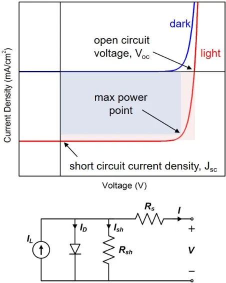
Figure 1.2: Current-voltage behavior and equivalent circuit of a solar cell.
Figure 1.2 shows the current-voltage behavior of a solar cell and illustrates
some important parameters that define solar cell performance. The
open-circuit voltage (VOC) is related to the band offsets between the n and p-type
materials as well as the quality of the interface. The short circuit current (JSC)
is a measure of the photocurrent collected by the solar cell. In addition, the
fill factor (FF) is a measure of the squareness of the J-V curve and is typically
1.2
Motivation for Cu
2O photovoltaics
Cuprous oxide (Cu2O) was one of the first known semiconductors, but its
po-tential application in photovoltaics was not seriously explored until alternative
materials for solar first garnered attention during the oil crisis of the 1970s.
[1] Many of Cu2O’s photovoltaic properties were characterized at that time,
however device efficiencies were limited by several factors, many of which are
still pertinent today. The second wave of research on earth-abundant solar
ma-terials came during the silicon crisis of the mid-2000s; however, current trends
seem to indicate that silicon is going to remain the dominant player in the solar
industry. One interesting advantage held by semiconductors like Cu2O that
have large bandgaps is that instead of competing with the dominant silicon
technologies, the addition of a Cu2O top cell to make a tandem cell stack can
potentially improve upon the performance of a crystalline silicon bottom cell.
In such a tandem configuration, the Cu2O solar cell needs to have a power
conversion efficiency above 8%. As we will see shortly, this is already a reality,
which makes Cu2O a highly relevant material. The detailed balance efficiency
limit for a single junction Cu2O solar cell has been calculated to exceed 20%
and for a dual junction with a crystalline Si bottom cell, this efficiency is 44%
[2].
Cu2O is composed of earth-abundant and non-toxic elements and can be
easily fabricated by oxidizing copper foils in air and cooling within the
ther-modynamic region of stability of the Cu2O phase. A thermodynamic phase
diagram is shown in Figure 1.3. A more detailed phase diagram of the high
temperature region can be found in [3]. This method of preparation has yielded
material with high absorption coefficient in the visible region, hole mobilities
exceeding 100 cm2V−1s−1, and minority carrier diffusion lengths in excess of
Figure 1.3: Thermodynamic phase diagram of Cu-O. [1]
1.3
Energy band alignment
Several important issues have impeded production of high efficiency Cu2O
devices. One of the main challenges stems from the intrinsically p-type nature
of Cu2O due to copper vacancy doping. This requires a heterojunction partner
material with a suitable energy band alignment in order to enable charge
separation in the device.
The low electron affinity of Cu2O (3.2 eV) limits potential heterojunction
candidates to those with similarly low conduction band edge energies. In
ad-dition, the small heat of formation of Cu2O (-170.7 kJ/mol) [6] means that
the surface is susceptible to reduction and oxidation. Prior work shows that
a stoichiometric Cu2O interface produces the highest efficiency devices [2, 7].
It is thus imperative to find a heterojunction partner material that has an
ap-propriate band offset and allows formation of a stoichiometric Cu2O interface.
Much of previous work has paired Cu2O with ZnO; however, the staggered
Voc to less than 600 mV, which is significantly less than the entitlement for
Cu2O of 1.5 V.
Recently, Ga2O3 [8, 9, 10], Zn(O,S) [2, 11, 12], and Zn1−xGexO [13] have
emerged as suitable heterojunction partner candidates for Cu2O due to their
favorable band alignment, and solar cells with open circuit voltages exceeding
1 V have been fabricated. Currently, the highest efficiency device, which
in-corporates a polycrystalline Cu2O absorber and a Zn1−xGexO buffer layer, is
8.1% [13].
What does an ideal band alignment look like for a heterojunction? Figure
1.4 shows idealized energy band positions for the components (a) in isolation,
and (b) after bringing the materials together after equilibration of the Fermi
level, EF. In order to maximize the open circuit voltage of the device, the
conduction band of the buffer layer needs to be slightly above the conduction
band of Cu2O, such that ∆EC is approximately 0.3 eV or less. This ensures
that electrons generated in the Cu2O by photon absorption can travel through
the buffer and window layers towards the front contact without experiencing
too much of a barrier. At the same time a slightly positive ∆EC will help
minimize surface recombination between the Cu2O and buffer. In the case of
the valence band offset, ∆EV, we want the valence band of the Cu2O to sit
much higher than the valence band of the buffer, which will block holes from
traveling into the buffer and causing recombination.
The heterojunction partners that have so far produced high open circuit
voltages, namely Ga2O3 and Zn(O,S), have demonstrated a slight positive
Figure 1.4: Idealized energy band positions for a heterojunciton solar cell with a p-type absorber (a) in isolation, and (b) after bringing the materials together. [14]
1.4
Scope of this thesis
This thesis seeks to identify and address the issues that limit photovoltaic
efficiency of Cu2O solar cells.
• Development of Cu2O growth by molecular beam epitaxy: We
have identified several undesirable properties in bulk thermally oxidized
wafers, as well as sputtered and electrodeposited thin films of Cu2O.
One way to overcome these issues is to use molecular beam epitaxy,
which is a UHV thin film growth technique that can potentially produce
high quality material by allowing precise control of growth parameters.
In chapter 2, we develop this technique to grow single phase, single
orientation thin films of Cu2O initially on MgO single crystals, which
are the closest lattice matched substrates and therefore ideal for epitaxy.
However, to make a solar cell we need to be able to contact the back
surface of the Cu2O film and since photolithography recipes have not
it heteroepitaxially on an ohmic contact material. In chapter 3, we use
bias-assisted sputtering to develop such templates. In chapter 4, we
explore growth of Cu2O by molecular beam epitaxy on these templates.
• Study of Cu2O/Zn(O,S) heterojunctions: In chapter 5 we explore
the suitability of Zn(O,S) as a heterojunction partner using Cu2O bulk
thermally oxidized wafers. We identify sources of high series resistance,
namely ZnSO4, which forms at the interface between Cu2O and Zn(O,S)
at low temperature. The formation of this undesirable, yet
thermody-namically favorable phase can be mitigated by depositing at elevated
substrate temperatures, and we find that 100◦C is the temperature at
which the short circuit current and the efficiency are maximized. We
also conduct light beam induced current measurements, which show that
bulk polycrystalline Cu2O devices exhibit grain-dependent photocurrent
collection and identify grain boundaries are photocurrent sinks.
• First devices incorporating MBE-grown Cu2O absorber: We
con-clude chapter 5 by fabricating and analyzing the first Cu2O/Zn(O,S)
so-lar cells made using molecuso-lar beam epitaxy to grow the Cu2O absorber
layer.
• Appendices: Oxide MBE and PLD user guides: Much of my time was spent using, fixing, and maintaining the oxide molecular beam
epi-taxy and the pulsed laser deposition systems. In an attempt to transfer
Molecular Beam Epitaxy of
Cu
2
O Thin Films on MgO
2.1
Introduction to Molecular Beam Epitaxy
The term “epitaxy” refers to growth of a crystalline film on a crystalline
strate, such that the crystallographic structure and orientation of the
sub-strate influences that of the film. [17, 18] Furthermore, growth of material A
on substrate B is referred to as “heteroepitaxy.” Molecular beam epitaxy is
a physical vapor deposition technique which is typically carried out in
ultra-high vacuum (UHV), i.e. at pressures below 10−9 Torr. The source material is
typically thermally evaporated from a solid or liquid elemental source, forming
a “molecular beam” that settles on the substrate. [19, 20, 21] When reactive
deposition of materials is necessary, process gases or plasma sources can be
added to the system. In the case of experiments detailed in this thesis, an
RF atom source is used to partially split O2 molecules into monatomic oxygen
using an RF plasma. These oxygen atoms can then travel to the substrate and
react to form oxides.
Figure 2.1 shows the basic layout of the system used in this thesis. The
system was home built by R. T. Brewer. [22]. A detailed procedure for
oper-ation of this instrument is presented in Appendix A. Samples are loaded into
the load lock and pumped down using a small turbo-drag pump. The samples
are then transferred into the main chamber, which is actively pumped by a
cryogenic pump operating at 11 K. The chamber is equipped with a residual
gas analyzer (RGA), which detects and quantifies the gaseous species present
in the chamber. The Cu source is a high temperature effusion cell with a
py-rolytic boron nitride conical crucible filled with 6N pure Cu metal pellets. The
vapor pressure of Cu is low in the solid phase, so the cell needs to be heated
[image:23.612.169.444.343.578.2]above 1200◦C to achieve an appreciable Cu flux.
Figure 2.1: Schematic of plasma-assisted MBE chamber.
2.1.1
Reflection high energy electron diffraction
(RHEED). The system consists of a focused electron beam of 15 - 20 keV
en-ergy that is incident on the sample at a grazing angleθ, as shown in Figure 2.2,
and a CCD camera that records the diffraction pattern incident on a phosphor
screen. Diffracted intensity is seen when the reciprocal lattice of the surface
material crosses the Ewald sphere. The resulting surface diffraction pattern
is very useful for determining the surface structure of both the substrate and
the growing film.
Figure 2.2: Ewald sphere construction of RHEED geometry.
Figure 2.3 shows the features typically seen in RHEED patterns. An
amor-phous surface would not show any features besides a diffuse scattering of
elec-trons. A polycrystalline sample will show a RHEED pattern consisting of rings
because the reciprocal space of a polycrystalline sample is a set of concentric
spheres, which, when crossing the Ewald sphere will appear as rings. A rough
but oriented crystalline surface will produce a three-dimensional transmission
electron diffraction pattern, similar to ones seen in TEM. When the film grows
in islands this is the most common pattern, as we will see later in this chapter.
The reciprocal space of a perfect surface consists of infinite rods in the
and other defects in the crystal. In addition, broadening of the Ewald sphere
itself can occur as a result of energy variations in the electron beam. Thus
the RHEED pattern of a single crystal consists of streaks. The streaks will be
shortened by presence of an non-zero offcut of the sample surface or atomic
[image:25.612.173.443.202.483.2]steps on the surface, with larger steps producing longer streaks.
Figure 2.3: Effect of film structure on RHEED pattern.
2.1.2
Thin film growth modes
The mode of growth of an epitaxial film depends on several factors, including
the surface structure and quality of the substrate, lattice mismatch between the
two materials, growth conditions such as temperature and flux, and energies
associated with all the possible interfaces. There are three basic growth modes
that can occur, and they are shown schematically in Figure 2.4. The
occurs when the surface energy of the substrate is higher than the interface
energy between the film and substrate and consequently the film atoms have a
strong preference for binding to the substrate. This mode is also characterized
by the presence of fast diffusion of surface atoms such that they can find the
lowest energy sites. The two-dimensional growth mode is typically preferred
because it yields the highest crystalline quality and smooth surfaces.
Figure 2.4: Thin film growth modes. Θ refers to monolayer (ML) coverage of the surface.
Initial layer-by-layer growth can turn into island growth in the
Stranski-Krastanov growth mode. This typically occurs due to a change in energetics
beyond a critical layer thickness, which is related to the chemical potential
of the film as well as strain. Once layer-by-layer growth breaks down, the
subsequent layers form from the nucleation and coalescence of islands. The
third growth mode is the island, or Volmer-Weber mode. This arises when
the film atoms are more likely to bind to each other than to the substrate.
2.2
Growth of Cu
2O on MgO
Arguably the strongest motivation for Cu2O in photovoltaic applications is its
relatively large band gap of 2.1 eV (and exciton gap at 1.9 eV), which make
it a promising candidate as a top cell in a tandem solar cell combined with a
crystalline silicon bottom cell. In order for such a tandem cell to improve upon
existing Si cell efficiency, a Cu2O cell efficiency approaching 10% is required
[23]. The development of such a structure would require synthesis by thin
film methods, and molecular beam epitaxy (MBE) provides precise control
over many deposition parameters and generally yields high quality material.
MBE synthesis of Cu2O on MgO substrates has been demonstrated using pure
atomic oxygen [24, 25, 26], however no reports of a diluted oxygen plasma have
been made to date. Also, growth on MgO (1 1 0) surface has been reported
by sputtering [27] and pulsed laser deposition [28], but not by MBE. DFT
calculations [29] show that the Cu2O (1 1 0) surface has the lowest energy,
so it is reasonable to assume that a substrate that promotes growth in this
direction may foster Cu2O phase stability over a larger range of deposition
parameters, and this is consistent with results of this work. We compare the
structural properties of Cu2O films grown using a pure oxygen atmosphere to
films grown using a 90%Ar/10%O2 premix, on (1 0 0) and (1 1 0) orientations
of MgO.
2.2.1
Experimental Setup
Thin films of CuxO were grown in a custom molecular beam epitaxy system
equipped with an Oxford RF atom source. RF atom sources dissociate
molec-ular species (such as O2 or N2) into atomic species for increased reactivity
are associated with creation of point defects. Ionic components of the plasma
that escape the atom source were further filtered out by ion deflection plates.
Thus the current of gas species was composed of atomic argon and/or oxygen.
Oxygen (Air Liquide, 99.9999% purity) partial pressure was varied between
1×10⁻⁷ and 1×10⁻⁵ Torr. For growths with argon/oxygen premix (Air Liq-uide, 99.9999% purity, 10.0% oxygen, balance argon), the gas partial pressure
of argon was correspondingly an order of magnitude higher. The presence of
argon allowed for stability of the plasma, while decreasing the partial pressure
of reactive oxygen species. Partial pressures were monitored by a residual gas
analyzer (RGA). Atom source plasma power was varied between 100 and 200
W and plasma optical emission voltage ranged from 1 V to 3 V during film
deposition. Plasma emission voltage corresponds to the intensity of light
emit-ted from the plasma and correlates with the efficiency of dissociation of the
molecular gas into its atomic components. The growth chamber base pressure
was <3×10⁻⁹ Torr. Copper metal (6N, Alfa Aesar) was evaporated from a
high temperature effusion cell at a temperature ranging from 1250-1300 ◦C.
CuxO was formed reactively at the surface of the substrate kept at a
tem-perature ranging from 400-650 ◦C. MgO was chosen as a substrate because
it is the closest lattice matched commercially available single crystal; it is
also refractory, transparent, and non-conductive, which makes it suitable for a
variety of electrical and optical characterization techniques. MgO substrates
were cleaned in situ by annealing at deposition temperature for an hour and subsequently plasma cleaned for 10 minutes. In situ reflection high energy electron diffraction (RHEED, with electron beam energy of 20 keV) was used
to confirm cleanliness and orientation of the substrate surface and monitor film
transmis-sion electron microscopy (TEM, FEI Tecnai F30 with S-TWIN objective, 300
keV electron energy), and atomic force microscopy (AFM, Asylum Research
MFP 3D). TEM cross sections were prepared using standard focused ion beam
milling on an FEI Versa 3D).
2.2.2
Growth using pure oxygen plasma
Figure 2.5: HRXRD spectra of CuxO films grown on MgO (1 0 0) at (a) 1×10⁻⁶
Torr and (b) 5×10⁻⁶ Torr oxygen, both cases corresponding to presence of undesirable phases and (c) pure phase Cu2O film grown on MgO (1 1 0) at
9×10⁻⁶ Torr.
Growth of CuxO on MgO was initially studied by varying oxygen partial
pressure (using pure oxygen gas) and substrate temperature, while fixing the
Cu effusion cell temperature at 1275 ◦C, atom source plasma power at 100
W, and plasma optical emission voltage at 1 V (which corresponds to the
lower range of stability of the plasma source). As illustrated in Figure 2.5
(a-b), the growth window for the Cu2O phase on MgO (1 0 0) was found to
be too narrow to reproducibly grow single phase films. Raising the pressure
of oxygen by only half an order of magnitude, while maintaining otherwise
identical growth parameters and low oxygen plasma power, changed the film
composition from a mixture of Cu2O and Cu to CuO. Figure 2.5 (c) shows that
single-phase epitaxial growth of Cu2O on MgO (1 1 0) is achievable within a
narrow range of deposition parameters using pure oxygen. It should be noted
are commonly present.
The difficulty of growing single phase, single orientation Cu2O on MgO
(1 0 0) has been demonstrated before, and it is known that the (1 1 0) MgO
orientation is more amenable to unidirectional Cu2O epitaxy, and regardless
of substrate orientation, growth of Cu2O in the (1 1 0) direction is usually
preferred compared to (1 0 0). Although reasons for this are still debated and
different epitaxial relationships have been reported [24, 25, 30, 31], density
functional theory calculations show that the Cu2O (1 1 0):CuO surface has the
lowest energy, and generally the nonpolar Cu2O (1 1 0) surfaces have lower
energies than the polar Cu2O (1 0 0) surfaces [29]. Lattice mismatch seems to
be less important than surface energy in determining the preferential growth
direction [24].
Figure 2.6: RHEED images of Cu2O growth on MgO using pure oxygen
plasma. (a) Plasma cleaned MgO (1 0 0) surface along the [1 1 0] azimuth, (b) 100 nm of Cu2O showing growth initiates and persists in the Volmer-Weber or
island regime and the pattern is a superposition of the Cu2O [1 1 1] and [2 1 1]
zone axis transmission patterns; (c) indexing of diffraction spots in (b) along [1 1 1] zone axis (black) and [2 1 1] zone axis (gray); (d) plasma cleaned MgO (1 1 0) surface along the [1 1 1] azimuth, (e) 10 nm of Cu2O along [1 1 1] again
initiates with island growth (for spot indexing refer to Fig. 2.6 (f)), (f) after 100 nm of Cu2O viewed along [1 1 1], islands merge into a smooth film with
steps, as evidenced by a streaky pattern.
Growth of Cu2O initiates with islands corresponding to two symmetrically
equivalent variants of the Cu2O (1 1 0) surface such that the pattern in Figure
2.6 (b) is a superposition of the Cu2O [1 1 1] and [2 1 1] zone axis transmission
patterns. Figure 2.6 (c) shows the schematic indexing of the diffraction spots.
These results are consistent with the literature results of Cu2O growth on
MgO (1 0 0) [24, 31]. Figure 2.6 (b) (d-f) shows that growth of Cu2O on MgO
(1 1 0) starts in the Volmer-Weber or island regime, and the islands eventually
merge to form a smooth and continuous film with some surface disorder as
evidenced by the streaky nature of the pattern [32]. Note that the RHEED
pattern corresponds to only a single orientation of the film, which indicates
that nucleation of the second orientation is not spatially uniform and most
likely predominates away from the center of the sample.
Despite some success in growing single phase Cu2O films on the (1 1 0) MgO
orientation, reproducibility was still an issue due to the limited oxygen partial
pressure growth window. The partial pressure of oxygen needed to produce a
stable plasma in the RF atom source needed to exceed 1×10⁻⁶ Torr, and the
growth window for pure Cu2O was found to be close to this limit for pure
oxy-gen. There are several ways to enable growth of single phase, single crystalline
orientation Cu2O, which include raising substrate temperature, raising the Cu
flux, and using a different oxidant. The substrate temperature was already
approaching the limits of the system, and higher growth temperature is
gener-ally undesirable in terms of substrate compatibility and cost. Raising the Cu
flux by increasing source filament temperature is also problematic in terms of
operation costs and effusion cell lifetime. Instead, oxygen partial pressure was
diluted using an inert balance gas (90%Ar/10%O2 premix) to enable stable
2.2.3
Growth using 90%Ar/10%O
2plasma
Figure 2.7 shows HRXRD data of various films of CuxO grown on (a) MgO
(1 0 0) and (b) MgO (1 1 0). The XRD peak intensities are lower compared
to those of Figure 2.5 because film thickness is substantially reduced using a
90%Ar/10%O2 gas mixture. Growth rate using pure oxygen at 550 ◦C was
measured by x-ray reflectivity to be 100 nm/hr, while growth using the Ar/O2
gas mixture was measured to be 20 nm/hr. For growth on MgO (1 0 0), Cu2O
Figure 2.7: HRXRD spectra of CuxO grown on (a) MgO (1 0 0) and (b) MgO
(1 1 0) using argon-oxygen plasma. Spectra are labeled with deposition tem-perature, plasma power, and plasma optical emission voltage.
films are obtained at low plasma optical voltages and powers, and intermediate
substrate temperatures. Plasma emission voltage, which is a function of gas
flow rate and plasma power, was found to better correlate with the epitaxial
film quality than either the gas flow rate or the plasma power. The epitaxial
growth phase diagram in Figure 2.8 (a) summarizes these results. As shown
in Figure 2.7, films grown on MgO (1 1 0) all have a single orientation in the
(1 1 0) Cu2O direction, for a wide range of plasma parameters and substrate
temperatures.
Figure 2.8: MBE regime phase diagram for growth of CuxO on (a) MgO (1 0 0)
and (b) MgO (1 1 0), using argon-oxygen plasma.
grown on MgO (1 0 0); growth starts in the Volmer-Weber island growth mode
and after 60 nm starts to smooth out into a continuous film as evidenced by
the appearance of streaks. Growth on the MgO (1 1 0) surface is shown in
Figure 2.9 (d-f). In contrast to films grown using pure oxygen that exhibited
two variants of the Cu2O (1 1 0) orientation, films grown using Ar/O2 exhibit
only one variant, at least within the region probed by the RHEED electron
beam. Looking at the [1 1 1] Cu2O azimuth in Figure 2.9 (e), all spots can be
indexed to the corresponding transmission diffraction pattern shown in Figure
2.9 (f), and no extra spots corresponding to the [2 1 1] azimuth are present.
The pattern looks very similar to that of Figure 2.6 (e). Growth remains
3-dimensional possibly due to the fact that the film thickness is not large enough
to completely cover the MgO surface, as seen in AFM and TEM examination
of the film in Figure 2.10.
The epitaxial relationship of Cu2O (1 1 0) on MgO (1 1 0) was confirmed
directly by TEM, as shown in Figure 5.5. The selected area diffraction pattern
in Figure 5.5 (b) shows the Cu2O lattice directly overlaps the MgO lattice and
Figure 2.9: RHEED images of Cu2O growth on MgO using argon-oxygen
plasma. (a) Plasma cleaned MgO (1 0 0) surface along the [1 1 0] azimuth, (b) 60 nm of Cu2O proceeds with island growth shown here along the [1 0 0]
azimuth, and islands start to merge into a smooth film, as evidenced by the appearance of streaks, but growth remains 3-dimensional, which may be at-tributed to lower film thickness than in the pure oxygen films. (c) schematic spot indexing along [100] zone axis of Cu2O. (d) Plasma cleaned MgO (1 1 0)
surface along the [1 1 1] azimuth, (e) 60 nm of Cu2O shown here along the
[1 1 1] azimuth showing growth initiates and persists in the island regime, (f) schematic spot indexing along the [1 1 1] zone axis of Cu2O.
Conclusion
Single phase, single orientation Cu2O thin films have been grown on MgO by
plasma-assisted molecular beam epitaxy using both pure oxygen and
argon-oxygen gas mixtures. Growth using argon-argon-oxygen opens up the stability
win-dow of the Cu2O phase by giving access to lower partial pressures of oxygen
while still maintaining a stable plasma. The film growth rate using
argon-oxygen is reduced compared to pure argon-oxygen; however film mosaicity and
tex-ture are also reduced, yielding a film with increased crystallinity. The results
of this work facilitate the development of high quality absorber layers for an
Figure 2.10: (a) AFM image of a 20 nm Cu2O film grown on MgO (1 1 0)
using an argon-oxygen plasma showing island-type film morphology. (b) TEM micrograph showing cross sectional morphology of Cu2O on MgO (1 1 0)
con-firming island-growth regime.
Figure 2.11: (a) High resolution cross-sectional TEM of (1 1 0) Cu2O on MgO
(1 1 0) viewed down the [1 1 1] zone axis shows epitaxial relationship between film and substrate. (b) Selected area electron diffraction pattern shows a superposition of the Cu2O [1 1 1] and MgO [1 1 1] zone axis diffraction patterns,
Heteroepitaxial Ohmic
Templates for Cu
2
O Growth
The crystallographic orientation of a metal affects its surface energy and
struc-ture, and has profound implications for surface chemical reactions and interface
engineering, which are important in areas ranging from optoelectronic device
fabrication to catalysis. However, it can be very difficult and expensive to
manufacture, orient, and cut single crystal metals along different
crystallo-graphic orientations, especially in the case of precious metals. One approach
is to grow thin metal films epitaxially on dielectric substrates. In this work,
we report on growth of Pt and Au films on MgO single crystal substrates of
(1 0 0) and (1 1 0) surface orientation for use as epitaxial templates for thin
film photovoltaic devices. We develop bias-assisted sputtering for deposition
of oriented Pt and Au films with sub-nanometer roughness. We show that
bi-asing the substrate decreases the substrate temperature necessary to achieve
epitaxial orientation, with temperature reduction from 600 to 350 ◦C for Au,
and from 750 to 550 ◦C for Pt, without use of transition metal seed layers. In
addition, this temperature can be further reduced by reducing the growth rate.
Biased deposition with varying substrate bias power and working pressure also
enables control of the film morphology and surface roughness.
3.1
Metal Films on Dielectric Substrates
Epitaxial growth of metal films on dielectric substrates has been the subject of
intense study due to its fundamental role in technologically important
appli-cations, such as optoelectronic devices and catalysis, as well as understanding
crystalline growth. Material properties can vary widely with surface
struc-ture and symmetry; however, oriented single crystals are expensive and often
unavailable. Therefore, thin film growth is a promising tool to study
orienta-tion dependence of material properties without having to manufacture single
crystalline samples. The purpose of this study was to develop oriented thin
films of Au and Pt on MgO single crystalline substrates for use as ohmic
het-eroepitaxial templates for growth of semiconductor oxides, such as cuprous
oxide, for thin photovoltaic applications. The requirements for a
heteroepi-taxial template include single film orientation and minimal surface roughness.
Typically, metals like Au and Pt tend to adapt the (1 1 1) orientation when
substrate effects are screened by surface contaminants, so high temperature
processing and careful surface preparation are required to achieve epitaxy for
other crystallographic orientations [33, 34]. In this work, we grow thin films
of Au and Pt in the (1 0 0) and (1 1 0) orientations with sub-nanometer
sur-face roughness on MgO substrates while reducing the substrate temperature
necessary for epitaxy using bias-assisted sputtering.
MgO is chosen as a substrate because it is transparent, refractive,
insulat-ing, and does not react with Pt or Au, forming a clean atomically flat interface.
which can form silicide precipitates at the interface and impact the
epitax-ial relationship [35]. MgO is also well lattice matched to many metals with
face-centered-cubic symmetry and can grow biaxially textured on amorphous
substrates, providing a path for large-area deposition of oriented films on
amor-phous substrates [36]. The use of Fe or Ni layers to seed cube-on-cube epitaxy
of Pt (1 0 0) on MgO (1 0 0) has been studied for catalysis applications [35];
however, these transition metals create deep level electronic defects in many
semiconductors, and so are of less interest for photovoltaic film applications.
Nucleation and growth of Pt and Au particles on MgO has been the subject
of intense study, and reviews exist on the subject [37]. Thin film growth of Pt
on MgO has been explored by molecular beam epitaxy [38], pulsed laser
depo-sition [35], electron beam evaporation [39], as well as sputtering [34, 40, 41].
Fewer studies of Au thin film growth on MgO exist [42], although nucleation
of Au particles has been studied extensively [43, 44, 45].
We chose sputter deposition because it is an economical and industrially
scalable process. In addition, sputtering allows for the use of substrate bias,
which has been shown to have many beneficial effects on film growth, including
in situ substrate cleaning and control over the energy of atoms impinging on
the surface citemattox. In this report, we show that substrate bias facilitates
epitaxial growth of Pt and Au films on MgO by increasing mobility of surface
adatoms, influencing the number and density of nucleation sites, increasing
film density, and disrupting columnar grain growth. These effects result in
Figure 3.1: Potential variation near a cathode for a DC discharge plasma.
3.2
Bias-assisted sputtering
During sputtering, target material is ablated by bombardment of energetic
ions. Ar is a common choice due to its low reactivity, low cost, and
appropri-ate atomic weight for many elements, while Ne is better suited for sputtering
lighter elements and Xe and Kr allow more efficient sputtering of heavier
ele-ments. The ejected target atoms impinge on the substrate forming a film. The
substrate can be left grounded or be negatively biased using an RF power
sup-ply — RF is necessary to prevent charging in electrically insulating substrates.
The purpose of negatively biasing the substrate is to modify the behavior of
charged particles in the vicinity of the substrate by controlling their flux and
energy. We can control and magnify the potential drop that normally occurs
between the plasma, which is slightly positive, and the substrate, thus
control-ling the electric field that can accelerate target atoms onto the growing film.
This is demonstrated schematically in Figure 3.1. In the case of RF bias, the
In order to understand the particle energies involved in sputtering, it is
useful to look at the mean free path (λ), or the average distance a particle
travels before colliding. The mean free path can be calculated using a simple
billiard ball model [47]:
λ= √ 1
2πd2n
where d is the effective particle diameter, and n is the gas density, which can
be calculated using the ideal gas law. The particle diameter of Ar is 3.64 ˚A
[48]. The mean free path at different temperatures and pressures relevant to
this study is shown in Table 3.1.
Table 3.1: Mean free path of Ar at different temperatures and pressures.
Pressure (mTorr) 25◦C 350◦C 550◦C 700◦C
1 5.2 cm 11 cm 14 cm 17 cm
3 1.7 cm 3.7 cm 4.8 cm 5.7 cm
5 1.0 cm 2.2 cm 2.9 cm 3.4 cm
7 0.7 cm 1.6 cm 2.1 cm 2.4 cm
At 1 mTorr, the mean free path of an Ar atom is approximately 5 cm
at room temperature, and increases as the temperature increases [47]. Thus
the mean free path is larger than the width of the dark space over which the
plasma is non-neutral and the electric field is largest, which was measured
to be approximately 3 cm. Thus Ar ions impinging on the substrate surface
at these conditions have energies corresponding to the bias potential plus the
plasma energy, which is typically on the order of 10 eV.
All of the films analyzed in this study were grown using a sputter
deposi-tion system with a base pressure of 1.3×10⁻⁷ Torr, shown schematically in
Figure 3.2: Sputtering system schematic.
sources. Substrate heating is provided by two halogen lamps situated behind
the substrate chuck plate.
Single crystal MgO substrates of (1 0 0) and (1 1 0) orientation purchased
commercially were annealed and cleaned in situ prior to deposition. The
im-portance of substrate surface preparation to epitaxy cannot be overstated,
particularly in the case of MgO, which is a highly hygroscopic material.
Com-mercially available MgO crystals are typically prepared by mechanical
polish-ing, which has been shown to amorphize the top few layers of the crystal and
therefore necessitates a high temperature oxidative anneal to reconstruct the
rocksalt structure and remove adventitious hydroxide. [49]
The substrates were heated to 700 ◦C in vacuum for an hour, and then
annealed in 5 mTorr of oxygen for another hour. The temperature was then
ramped down at 30◦C/minute to the deposition temperature. The substrates
were plasma cleaned with a RF substrate bias of 30 W (corresponding to a
This cleaning procedure was found to result in clean MgO surfaces, as
evi-denced by reproducibly achieving an epitaxial relationship between the film
and substrate.
Pt or Au thin films were then deposited at 100 W DC power. Substrate
temperature, working pressure, and RF substrate bias magnitude were varied
during the study. Temperature was ramped down at a rate of 30 ◦C/min
directly following deposition. All samples had a film thickness around 50 nm,
as measured by x-ray reflectivity. Films were characterizedex situ using high-resolution x-ray diffractometry (HRXRD) and non-contact ambient atomic
force microscopy (AFM).
3.3
Growth of Pt and Au on MgO by
Bias-Assisted Sputtering
Figure 3.3 shows the orientation relationship between (a) Pt and (b) Au films
grown on MgO (1 0 0) and (1 1 0) single crystals. All films in this figure were
deposited with an RF substrate bias of 15W (corresponding to 180 eV
imping-ing atom energy). For the case of Pt films, at 500 ◦C both MgO orientations
exhibit Pt (1 1 1), which disappears completely for 550 ◦C, resulting in
epi-taxially oriented Pt films on MgO. For the case of Au films, at 300 ◦C, the
(1 1 1) orientation has the highest intensity on both MgO (1 0 0) and (1 1 0)
substrates. At 350◦C, the dominant orientation is aligned with the substrate
for both (1 0 0) and (1 1 0) MgO orientations. Although we never completely
eliminate the Au (1 1 1) for growth on MgO (1 0 0), the relative magnitude of
this peak suggests that the fraction of (1 1 1) orientation is less than 1%. It is
important to note that without substrate bias, the temperatures necessary to
Figure 3.3: X-ray diffraction spectra of (a) Pt films on MgO (1 0 0) and (1 1 0), and (b) Au films on MgO (1 0 0) and (1 1 0). Black circles (•) indicate substrate peaks.
for Au.
Figure 3.4 (a) shows the φ scan of the Pt (1 0 0) film deposited at 550 ◦C
and MgO substrate collected at a ψ tilt of 54.74◦ such that the {1 1 1} planes satisfy the diffraction condition. Figure 3.4 (b) shows the φ scan of the Pt
(1 1 0) film deposited at 550 ◦C and MgO substrate collected at a ψ tilt of
35.26◦ such that the {1 1 0} planes satisfy the diffraction condition. The film is again epitaxially oriented with the substrate. The φ scans for Au (1 0 0)
and (1 1 0) films show the same symmetry as that seen for Pt films. Based on
these in-plane and out-of-plane orientation relationships, we conclude that the
epitaxial relationship is cube-on-cube, i.e., (1 0 0)/(1 0 0) and (1 1 0)/(1 1 0).
In addition to being able to grow oriented Au and Pt films on MgO, it is
essential for epitaxy that these films have minimum roughness. To provide a
reference, AFM topography scans were used to measure the surface roughness
of the MgO substrate before and after substrate cleaning by RF etching.
Sev-eral literature studies suggest that an increase in substrate surface roughness
sup-Figure 3.4: (a) φ scans of Pt (1 0 0) films showing Pt and MgO {1 1 1} at
ψ=54.74◦ showing in-plane symmetry, and (b)φscans of Pt (1 1 0) films show-ing Pt and MgO{1 1 0} atψ=35.26◦.
press nucleation of the Pt (1 1 1) orientation [50, 51]. However, in our study the
root-mean-square roughness (rRMS) decreased after the substrate clean. For
MgO (1 0 0), rRMS decreased from 0.36 nm to 0.20 nm, and for MgO (1 1 0),
rRMS decreased from 0.17 nm to 0.13 nm. Thus we conclude that the main
result of the substrate treatment, which includes heating to 700 ◦C, annealing
in oxygen, and plasma etching the substrate, is the removal of adventitious
surface contamination instead of increase of surface roughness. Without the
plasma cleaning prior to deposition, we could not reproducibly achieve
epi-taxial orientation until heating to very high substrate temperatures and Pt
and Au (1 1 1) orientation was frequently present even in these circumstances,
indicating that the absence of surface contamination is essential in achieving
an epitaxial growth relationship.
Figure 3.5 shows the morphological features of the surface, as well as the
root-mean-square roughness of Pt films deposited on different orientations of
tempera-ture while maintaining a working pressure of 3 mTorr Ar, a substrate bias of
15 W, and a target power of 100 W. At 500 ◦C, when based on XRD
anal-ysis the film is composed of multiple crystallographic orientations, including
(1 0 0), (1 1 0), and (1 1 1), the film morphology consists of three-dimensional
islands and the roughness is on the order of a few nanometers. As the
tem-perature is increased to 550 ◦C, and substrate-film interactions dominate the
orientation relationship resulting in epitaxial growth, the morphology of the
film changes drastically. In the case of the (1 0 0) MgO surface, rectangular
grains with sides oriented along h1 1 0i form a crossing pattern, and the films have sub-nanometer roughness of approximately 5 ˚A. In the case of the (1 1 0)
MgO surface, rectangular grains again grow along h1 1 0i; however, no cross-ing of grains is evident and they are all oriented along the same direction.
Film roughness is greater for this substrate orientation, at around 1.3 nm. As
the substrate temperature increases, grain size increases as well, and therefore
film roughness also increases. In order to attempt to decrease the roughness
of Pt films grown on MgO (1 1 0), we adjusted working pressure and substrate
bias while keeping the substrate temperature at 550◦C, which was the lowest
temperature at which epitaxy occurs for the given growth rate. The results,
illustrated in Figure 3.5 (b), show that increasing the substrate bias from 15
W to 30 W, or increasing the working pressure from 3 mTorr to 7 mTorr,
or the combination of both, decreases surface roughness of the films into the
sub-nanometer range. This can be explained by the increase in the number of
heterogeneous nucleation sites due to both higher pressure, and higher energy
of atom bombardment. Figure 3.5 (b) also indicates that for growth on MgO
(1 0 0) surfaces, increasing substrate bias while keeping working pressure
con-stant increases grain size. Increased substrate bias effectively raises the energy
Figure 3.5: AFM topography maps of Pt films on MgO (1 0 0) and (1 1 0) deposited under different conditions. Families of directions h1 0 0i and h1 1 0i denote direction normal to the substrate surface, as well as the horizontal and vertical directions in the AFM images. (a) Effect of changing substrate temperature while maintaining a working pressure of 3 mTorr and bias of 15 W. (b) Effect of changing substrate bias and working pressure while maintaining substrate temperature at 550 ◦C.
of surface adatoms settling into the lowest available energy sites, thus
pro-moting grain growth. In contrast, raising working pressure while maintaining
the same substrate bias results in smaller grains due to a larger number of
nucleation sites for the film and a decrease in the energy of atoms hitting the
surface.
Figure 3.6 shows the morphological features of Au films grown on MgO.
At 300 ◦C, when the film exhibits multiple orientations, the film structure is
dominated by three-dimensional islands and the roughness is about 20 nm.
As the temperature is increased to 350 ◦C, and an epitaxial relationship is
Figure 3.6: AFM topography maps of Au films on MgO (1 0 0) and (1 1 0) deposited at different substrate temperatures. All images are 5 µm by 5 µm.
(1 0 0) substrate. However, on the MgO (1 1 0) surface, Au islands do not form
a continuous film, and therefore the roughness is on the order of film thickness.
This is due to the high surface energy of the MgO/Au interface. Growing at
higher working pressures and with larger bias did not result in smooth films
appropriate for epitaxy.
Lastly, there have been literature reports showing that the substrate
tem-perature required to achieve an epitaxial relationship decreases as the growth
rate decreases [50, 51]. Therefore, we looked at the effect of deposition rate
on the temperature at which the (1 1 1) orientation disappears and the
cube-on-cube orientations start to dominate. Figure 3.7 demonstrates the effect of
deposition rate on the orientation relationships for (a) Pt on MgO grown at
Figure 3.7: Effect of target power on the orientation relationships for (a) Pt on MgO grown at 500 ◦C and (b) Au on MgO grown at 300 ◦C. A decrease in substrate power, with a corresponding decrease in growth rate, promotes an epitaxial relationship.
by changing the target power from 100 W to 25 W, keeping other deposition
parameters constant. The corresponding decrease in growth rate for Pt is from
0.8 ˚A/s to 0.2 ˚A/s, and for Au is from 1.5 ˚A/s to 0.4 ˚A/s. It is indeed the case
that a lower target power, and correspondingly a lower growth rate, promotes
growth of epitaxial films in both Pt and Au.
Conclusion
The main results of this work illustrate the effects of substrate preparation,
temperature, and bias, on the morphology of Pt and Au thin films grown on
single crystalline MgO substrates of (1 0 0) and (1 1 0) orientation. We
estab-lish an effective in situ substrate preparation and cleaning technique for MgO.
Introduction of substrate bias during film growth provides a way to control film
morphology and encourage an epitaxial growth relationship. Proper substrate
preparation and bias during deposition allow us to decrease the temperature
550 ◦C for Pt. This temperature can be further decreased by decreasing the
growth rate. We achieve sub-nanometer film roughness needed to make these
films suitable as epitaxial templates for device fabrication. In addition, we
illustrate the effects of changing the magnitude of substrate bias and working
Cu
2
O Growth on
Heteroepitaxial Ohmic
Templates
4.1
MBE of Cu
xO on Pt
In this chapter, CuxO thin films are deposited by plasma-assisted molecular
beam epitaxy (MBE) on noble metal heteroepitaxial templates, which were
developed in Chapter 3. We focus this study on Pt because it produces
con-tinuous, oriented thin films with sub-nm roughness for both MgO (1 0 0) and
(1 1 0) orientations. Some results on Au thin films are also included, although
only the Au (1 0 0) orientation successfully produced a sub-nm continuous film.
MgO is used as a heteroepitaxial template for the growth of CuxO
heterostruc-tures because it is a close lattice match to both FCC metals and CuxO and
can be grown biaxially textured on an amorphous substrate [36], providing a
path to dual junction cells.
Thin films of CuxO were deposited by plasma-assisted MBE with chamber
base pressure around 3x10⁻⁹ Torr, using an evaporation cell with Cu metal
and a pure oxygen plasma provided by an Oxford RF Atom source.
Deposi-tion pressure during growth was kept at approximately 1.5x10⁻⁵ Torr oxygen,
with plasma power around 150 W and plasma optical emission voltage (which
correlates with the efficiency of dissociation of O2 gas into its atomic
com-ponents) kept under 1 V. These conditions were found to stabilize the CuxO
phase. The substrates were heated to 550 ◦C and annealed in vacuum for 30
minutes prior to deposition of CuxO. Substrate temperature was kept at 550
◦C during deposition. Reflection high energy electron diffraction (RHEED)
with a 15 keV electron beam was used to monitor film structure in situ during
growth. Films were grown for 1 hour, which resulted in a thickness of
approx-imately 150 nm. Films were cooled in vacuum at a rate of approxapprox-imately 15
◦C per minute and analyzed ex situ using x-ray diffraction and non-contact ambient AFM. As we will show, the stability window of the Cu2O phase needs
to be re-optimized for every substrate orientation.
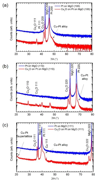
Figure 4.1 (a) shows the x-ray diffraction spectra of CuxO thin films
de-posited on Pt (1 0 0), which was sputtered on MgO (1 0 0). The Cu2O film is
primarily oriented in the (1 0 0) direction with some (1 1 1) orientation present.
The polar (1 0 0) surface of Cu2O is favored by the epitaxial relationship to the
Pt (1 0 0) film; however, the nonpolar hkl(111) surface of Cu2O is lower energy
than the polar (1 0 0) surface [29] and is typically present as well. It may also
be present due to a small amount of Pt (1 1 1) that can be seen in the x-ray
diffraction data of the original Pt template. There is also a wide shoulder on
the Pt (2 0 0) peak corresponding to formation of an alloy of Cu and Pt, which
is expected based on the thermodynamic phase diagram in Figure 4.2. The
alloy poses no issue as long as there is no shunting and the contact remains
Figure 4.1: HRXRD of CuxO films grown on Pt heteroepitaxial templates (a)
Figure 4.2: Phase diagram of Cu-Pt system. [52]
with the Cu2O film resistance on the order of 200 Ω.
Figure 4.1 (b) shows the x-ray diffraction spectra of CuxO thin films
de-posited on Pt (1 1 0), which was sputtered on MgO (1 1 0). Unlike the (1 0 0)
case, this orientation promotes formation of the monoclinic CuO phase, which
can be assigned to the unlabeled peaks. Growth on Pt (1 1 1), based on MgO
(1 1 1), is shown in Figure 4.1 (c). While the Cu2O phase has a single
orien-tation (1 1 1) and the peak is relatively sharp with a small FWHM, there are
several undesirable features. Atom mobility along close-packed planes in
cu-bic materials is higher, which may lead to increased alloy formation, as shown
by the larger magnitude of the Pt-Cu alloy peak. In addition, there is now
evidence of Cu formation, which is problematic for device performance.
Figure 4.3 shows the nucleation morphology and RHEED patterns of a
Cu2O film grown on Pt (1 0 0). The RHEED images indicate that the sputtered
Figure 4.3: RHEED and AFM images of Cu2O on Pt (1 0 0).
size is on the order of about 100 nm or larger on average. This is confirmed
by AFM topography scans of Chapter 3. Cu2O growth initiates in island
growth mode as evidenced by the spotty nature of the RHEED pattern at a
thickness of about 5 nm. At around 10 nm, the RHEED pattern starts to
exhibit streaks, which indicates a two-dimensional growth mode. This growth
mode dominates until the individual islands merge; however, at 150 nm the
RHEED pattern once again shows spots, which means there is a small growth
window for the two-dimensional mode, but that easily breaks down into island
grain size exceeds that of the underlying Pt film.
Figure 4.4: RHEED images of Cu2O on (a) Pt (1 1 0) and (b) Pt (1 1 1).
Figure 4.4 (a) shows surface structural properties of Cu2O deposited on
Pt (1 1 0). As can be seen from the RHEED images, the Pt film grown on
MgO (1 1 0) is rougher than that grown on MgO (1 0 0), and the resulting
Cu2O film is also rough as shown by the wide RHEED spots after 5 nm of
deposition. After 150 nm, growth is predominantly in the (1 1 0) direction;
however, multiple orientations as well as the presence of the CuO phase cause
the film to be highly polycrystalline, as evidenced by the appearance of rings in
the RHEED pattern. Under these conditions, the Pt/MgO (1 1 0) orientation
is less favorable for growth of phase pure Cu2O, however further optimization
of growth parameters may yield more favorable results. Figure 4.4 (b) shows
RHEED images of the Pt (1 1 1) template and subsequent growth of Cu2O.
The Pt (1 1 1) surface is very smooth, and has a roughness lower than both
the Pt (1 0 0) and (1 1 0) surfaces, as indicated by long and narrow streaks in
but has a single orientation, with the zone axis corresponding closely to [1 1 2].
Figure 4.5 shows two cross-sectional bright field TEM micrographs of a
Cu2O film grown on Pt (1 0 0) on MgO, corresponding to different sections
of the same film. The MgO/Pt and Pt/Cu2O interfaces appear to be very
smooth and flat, and the Pt film thickness is highly uniform. The Cu2O film
has a three-dimensional structure, with facets clearly shown in (a). There is
a defective layer at the interface between Cu2O and Pt that may be due to
epitaxial strain relaxation; this layer is on the order of 50 nm. In part (b)
the Cu2O layer appears to have some beam-induced recrystallization, which is
likely due to damage cause by the focused ion beam during sample preparation.
Figure 4.5: (a) Cross sectional TEM of CuxO grown by MBE on a sputtered
heteroepitaxial template of Pt on MgO, (b) different area of the same sample.
High resolution TEM micrographs of the (a) Pt/MgO interface and (b)
the Pt/Cu2O interface are shown in Figure 4.6. The Pt/MgO interface has a
strained layer that’s less than 5 nm thick and the two lattices seem to be in
registry, confirming epitaxial growth. The Pt/Cu2O interface exhibits a higher
degree of roughness, but the interface is still relatively sharp and although some
chemical mixing is present, as shown by x-ray diffraction studies, there is still
Figure 4.6: (a) Interface between Pt and MgO, (b) interface between Pt and Cu2O. Zone axis ish1 0 0i.
Selected area diffraction patterns are shown in Figure 4.7. These patterns
were acquired using a 10 µm selected area aperture, beam spot size 8, and 4
second exposure time. Selecting only the Pt film and MgO substrate yields the
pattern in (a). The zone axis is h1 0 0i and growth of Pt appears to be “cube-on-cube.” Figure 4.7 (b) includes contributions from the Cu2O, Pt, and MgO.
Since Cu2O is simple cubic, there are no reflections absent due to structure
factor rules, which limit the mixed odd and even (h, k, l) from appearing in
Figure 4.7: (a) Selected area diffraction pattern of Pt film on MgO, (b) selected area diffraction of a Cu2O film deposited on Pt on MgO.
4.2
MBE of Cu
2O on Au
Growth of Cu2O on Au sputtered films was also investigated. XRD spectra
in Figure 4.8 show that the Cu2O films on Au are highly oriented, just like
on Pt. In chapter 3 we found that the Au (1 1 1) orientation persists even at
high temperature, and the x-ray spectra of Figure 4.8 show a large Au (1 1 1)
peak on MgO (1 0 0). This results in growth of predominantly Cu2O (1 1 1),
with some (1 0 0) and (1 1 0). Interestingly, there is no alloy peak for Cu-Au,
although it is expected based on the phase diagram for these elements [53].
As shown in Figure 4.8 (b), the (1 1 0) substrate orientation leads to a single
phase, single orientation Cu2O (1 1 0) film, again with no peak for Cu-Au alloy.
While this indicates that growth of phase pure Cu2O films may be easier to
achieve on Au than on Pt in a wider growth parameter window, we found in
chapter 3 that the Au (1 1 0) film is not continuous on MgO under the growth
Figure 4.8: HRXRD of CuxO films grown on Au heteroepitaxial templates of
(1 0 0) and (1 1 0) orientation.
Cu
2
O Device Synthesis and
Characterization
[image:60.612.110.494.411.612.2]5.1
Device Preparation Scheme
Figure 5.1: Solar cell fabrication scheme.
Figure 5.1 illustrates the basic device fabrication procedure. Polycrystalline
Cu2O wafers were produced from 6N purity Cu foils, which were heated in a
quartz tube furnace to 1025 ◦C under N2 flow for 4 hours. The foils were
then oxidized in air for 24 hours and cooled under N2 flow to room
temper-ature. Cu foil thickness was 0.5 mm and the final Cu2O wafer thickness was
approximately 0.8 mm, with typical carrier concentration of 101
![Figure 1.3: Thermodynamic phase diagram of Cu-O. [1]](https://thumb-us.123doks.com/thumbv2/123dok_us/15620.1122/18.612.147.468.68.311/figure-thermodynamic-phase-diagram-of-cu-o.webp)


![Figure 4.2: Phase diagram of Cu-Pt system. [52]](https://thumb-us.123doks.com/thumbv2/123dok_us/15620.1122/53.612.136.476.82.337/figure-phase-diagram-of-cu-pt-system.webp)