5-12-2014
Digital Circuit Projects: An Overview of Digital
Circuits Through Implementing Integrated Circuits
- Second Edition
Charles W. Kann Gettysburg College
Follow this and additional works at:https://cupola.gettysburg.edu/oer
Part of theDigital Circuits Commons, and theSystems Architecture Commons Share feedbackabout the accessibility of this item.
This open access book is brought to you by The Cupola: Scholarship at Gettysburg College. It has been accepted for inclusion by an authorized administrator of The Cupola. For more information, please [email protected].
Kann, Charles W., "Digital Circuit Projects: An Overview of Digital Circuits Through Implementing Integrated Circuits - Second Edition" (2014).Gettysburg College Open Educational Resources. 1.
Description
Digital circuits, often called Integrated Circuits or ICs, are the central building blocks of a Central Processing Unit (CPU). To understand how a computer works, it is essential to understand the digital circuits which make up the CPU. This text introduces the most important of these digital circuits; adders, decoders, multiplexers, D flip-flops, and simple state machines.
What makes this textbook unique is that it puts the ability to understand these circuits into the hands of anyone, from hobbyists to students studying Computer Science. This text is designed to teach digital circuits using simple projects the reader can implement. But unlike most lab manuals used in classes in Digital Circuits or Computer Organization classes, this textbook is designed to remove the barrier of a laboratory
infrastructure needed in a face-to-face environment at a college or university. This textbook is designed to be used by the reader to create the circuits in their own homes. The textbook is free. The cost of the kits needed to do the labs is reasonable. And the projects are well documented and can be implemented by even novices to electronic projects.
This text allows professors to add laboratory projects in digital circuits to students in online classes in Computer Organization. This enhances these classes with interesting and fun exercises that reinforce the classroom topics.
This text can also be used by a hobbyist who wants to learn more about digital circuits and how computers work. The material is presented at a level that someone with no experience in digital circuits and electronics can successfully complete the projects, and gain an understanding of the circuits which go into making up a computer.
The second edition of this includes a chapter on Boolean Algebra for professors who would like to include a more formal background into digital circuits. It also changed the chapter designed to give a context for the CPU to reference a relatively simple CPU developed by the author in Logisim.
For someone who is interested in digital circuits, this book is worth downloading.
Note: Often it is easier to use a MS Word file rather than a pdf file. If you would like the book as a Word document and not a pdf, please contact the author at ckann(at)gettysburg.edu, and he will mail it to you. The main reason for this is to get some sort of feedback on who is using the text.
Keywords
Digital Circuits, System Architecture, Computer Organization, Integrated Circuits, Computer Logic, Central Processing Unit (CPU), Processor Architecture, Multiplexer, Decoder, Arithmetic Logic Unit, Register File, Flip-Flop, Memory, Memory Latch, Adder, Full Adder, Half Adder, State Computer, State Machine, Mod 4 Counter, 7400 Series, Digital Circuit Lab Manual, Electronic Circuits, Electronic Projects, Digital Circuit Projects, Computer Science Online, Online Laboratory Manual, Laboratory Manual
Disciplines
Digital Circuits | Systems Architecture
Please contact the author [email protected] you adopt this book for a course - thanks!
Creative Commons License
This work is licensed under aCreative Commons Attribution 4.0 License.
DIGITAL CIRCUIT
PROJECTS
Understanding Digital Circuits through Implementation Second Edition
ABSTRACT
This text explains some of the most basic digital circuits by implementing them on a breadboard. The use of the circuits in a CPU is then illustrated. This text is intended as a laboratory manual for a class is Computer Organization, or for use by a hobbyist who just wants to learn more about computer hardware.
Charles W. Kann
© Charles W. Kann III 277 E. Lincoln Ave. Gettysburg, Pa
All rights reserved.
This book is licensed under the Creative Commons Attribution 4.0 License
This book is available for free download from http://cupola.gettysburg.edu/oer/1/.
Table of Contents
Chapter 1 Before you start... 13
1.1 Introduction ... 13
1.2 Computers and magic ... 13
1.3 Reading this text ... 14
1.4 Materials Needed ... 14
1.4.1 Logisim ... 14
1.4.2 Hardware ... 14
1.5 Some notes ... 16
1.6 Conclusion ... 17
Chapter 2 Background Material ... 19
2.1 Introduction ... 19
2.2 A Universal Set of Boolean Operations ... 19
2.3 Truth Tables ... 20
2.4 Disjunctive Normal Form(DNF) ... 21
2.4.1 Boolean Relationships ... 22
2.5 Karnaugh Maps (K-maps) ... 23
2.5.1 Gray Codes ... 23
2.5.2 2-Variable Karnaugh Maps ... 24
2.5.3 3-Variable Karnaugh Maps ... 25
2.5.4 4-Variable Karnaugh Maps ... 27
2.5.5 Don’t care conditions ... 30
2.6 Conclusion ... 31
2.7 Exercises ... 32
Chapter 3 Getting started ... 35
3.1 Introduction ... 35
3.2 Logisim circuit to turn on a light ... 35
3.3 Implementing the switch circuit to turn on a light ... 36
3.3.1 The breadboard... 37
3.3.2 Stripping wires ... 38
3.3.3 Powering the Circuit ... 40
3.3.4 Installing the switch ... 43
3.3.5 Completing the Circuit ... 44
3.4 Debugging the circuit ... 45
4.1 Introduction ... 47
4.2 Boolean logic and binary values ... 47
4.3 Unary operations ... 47
4.4 Binary Operations ... 48
4.5 Implementing the AND gate circuit ... 49
4.5.1 ICs and the 7408 chip ... 49
4.5.2 The datasheet ... 50
4.5.3 Creating the AND circuit ... 51
4.6 Exercises ... 52
Chapter 5 Associative Boolean operators ... 55
5.1 Introduction ... 55
5.2 Modeling associative operations in Logisim ... 55
5.3 Implementing the circuit ... 56
5.3.1 Implementing the serial AND circuit ... 56
5.3.2 Implementing the parallel AND circuit ... 58
5.4 Conclusion ... 58
5.5 Exercises ... 58
Chapter 6 Adders ... 61
6.1 Introduction ... 61
6.2 Half adder ... 61
6.2.1 Adding binary numbers ... 61
6.2.2 Half adder circuit ... 62
6.2.3 Half adder implementation ... 63
6.3 Full adder ... 64
6.3.1 Full adder circuit ... 65
6.3.2 Full adder implementation ... 66
6.4 2-bit adder circuit ... 68
6.5 Conclusion ... 69
6.6 Exercises ... 69
Chapter 7 Decoders ... 71
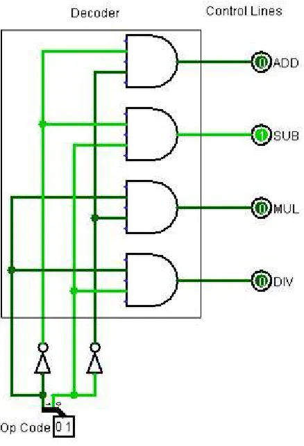
7.1 Introduction ... 71
7.2 Decoder circuit ... 71
7.3 2-to-4 decoder implementation ... 72
7.4.1 The 74139 chip ... 74
7.4.2 Implementing one 2-to-4 decoder using the 74139 chip ... 76
7.5 Conclusion ... 77
7.6 Exercises ... 77
Chapter 8 Multiplexers ... 79
8.1 Introduction ... 79
8.2 Circuit Diagram for a MUX ... 81
8.3 Implementing a MUX ... 83
8.4 74153 MUX chip ... 85
8.5 74153 circuit diagram ... 85
8.6 Implementing the 74153 circuit ... 86
8.7 Conclusion ... 87
8.8 Exercises ... 87
Chapter 9 Memory basics - flip-flops and latches ... 89
9.1 Introduction ... 89
9.2 Background material ... 89
9.2.1 State ... 89
9.2.2 Static and dynamic memory ... 90
9.2.3 Square Wave ... 90
9.3 Latches ... 90
9.3.1 D latch ... 91
9.3.2 Circuit diagram for a D latch ... 92
9.3.3 Implementing the D latch ... 93
9.3.4 D latch as a single IC chip ... 95
9.3.5 Implementation of a D latch using a 7475 chip ... 96
9.3.6 Limitations of the D latch ... 96
9.4 Edge triggered flip-flop ... 98
9.5 Conclusion ... 100
9.6 Exercises ... 100
Chapter 10 Sequential circuits ... 101
10.1 Introduction ... 101
10.2 Debouncing ... 101
10.3 Implementing a state machine ... 102
10.3.1 Mod 4 counter ... 102
10.3.4 Read Only Memory ... 105
10.3.5 Implementation of the Mod 4 counter ... 106
10.4 Conclusion ... 109
10.5 Exercises ... 109
Chapter 11 Use of these ICs in a CPU ... 111
11.1 An overview of the CPU. ... 111
11.2 Flip Flops ... 112
11.3 Muxes ... 112
11.4 Adder ... 112
11.5 Decoder ... 113
Table of Figures
Figure 3-1: Logisim circuit to turn on light. ... 36
Figure 3-2: Typical breadboard... 37
Figure 3-3: Breadboard layout ... 38
Figure 3-4: Wire strippers ... 39
Figure 3-5: A stripped wire ... 40
Figure 3-6: 7805 voltage regulator... 41
Figure 3-7: Powering the breadboard ... 41
Figure 3-8: LED ... 42
Figure 3-9: Toggle switch ... 43
Figure 3-10: Completed circuit ... 44
Figure 3-11: Debugging the circuit ... 45
Figure 4-1: Buffer and inverter gates ... 48
Figure 4-2: Buffer and inverter circuit in Logisim ... 48
Figure 4-3 Truth table for AND and OR ... 48
Figure 4-4: AND, OR, and XOR gates ... 49
Figure 4-5: AND, OR, and XOR gate circuit ... 49
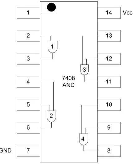
Figure 4-6: 7408 chip, circle indicates top of chip. ... 50
Figure 4-7: 7408 chip, notch indicates top of chip. ... 50
Figure 4-8: 7408 pin configuration diagram ... 51
Figure 4-9: 7408 AND gate circuit ... 52
Figure 5-1: Serial AND circuit ... 55
Figure 5-2: Parallel AND circuit ... 56
Figure 5-3: 7408 pin configuration diagram ... 57
Figure 5-4: Serial AND implementation ... 57
Figure 5-5: Parallel AND implementation ... 58
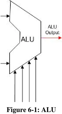
Figure 6-1: ALU ... 61
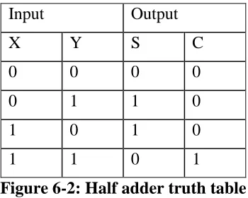
Figure 6-2: Half adder truth table ... 62
Figure 6-3: Half adder circuit ... 62
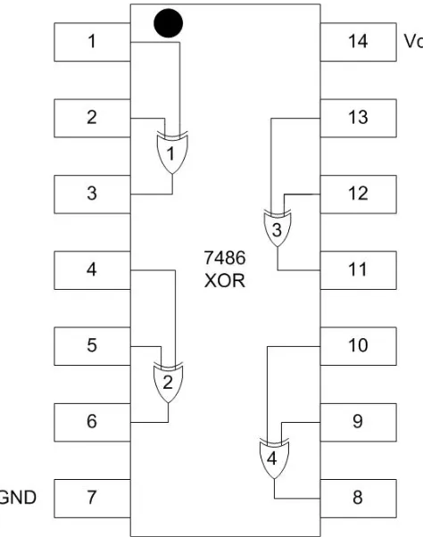
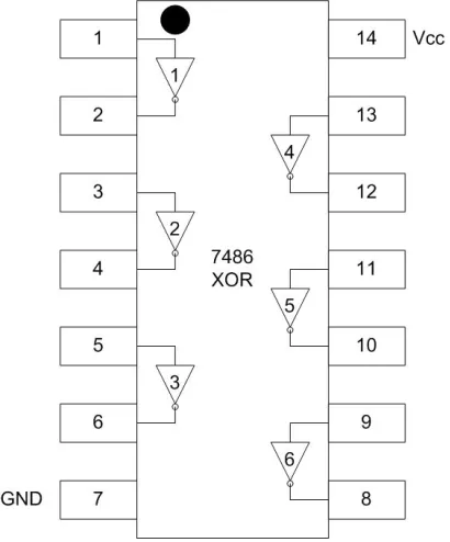
Figure 6-4: 7486 pin configuration diagram ... 63
Figure 6-5: Half adder implementation ... 64
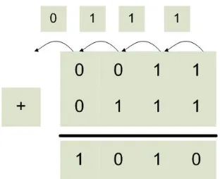
Figure 6-6: Addition problem showing a carry bit... 65
Figure 6-7: Full adder truth table ... 65
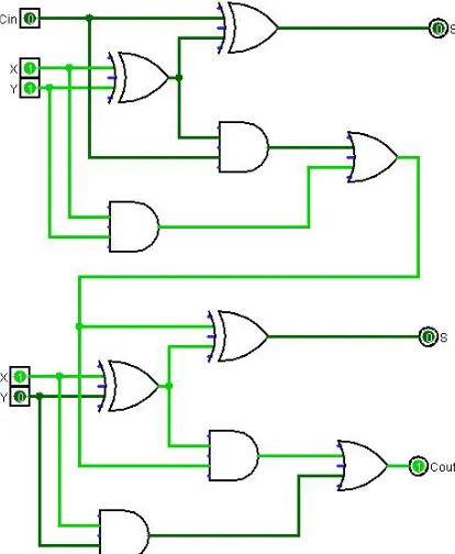
Figure 6-8: Full adder circuit ... 66
Figure 6-9: Full adder implementation ... 67
Figure 6-10: 2 bit full adder circuit ... 68
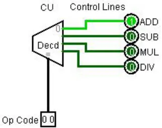
Figure 7-1: Control lines for ALU ... 71
Figure 7-2: Decoder used to set ALU control lines ... 71
Figure 7-3: Decoder circuit ... 72
Figure 7-4: 7404 pin configuration diagram ... 73
Figure 7-5: Decoder circuit ... 74
Figure 7-6: 74139 pin configuration diagram ... 75
Figure 7-7: 74139 decoder circuit ... 76
Figure 8-1: Multiplexer as a memory selector ... 79
Figure 8-2: Truth table for a MUX ... 80
Figure 8-3: 1-bit 4-to-1 MUX ... 80
Figure 8-6: Schematic of a MUX ... 82
Figure 8-7: Decoder used to implement a MUX ... 83
Figure 8-8: 4-to-1 MUX ... 84
Figure 8-9: 74153 circuit diagram ... 85
Figure 8-10: 74153 pin configuration diagram ... 86
Figure 8-11: 74153 circuit ... 87
Figure 9-1: Memory in a CPU ... 89
Figure 9-2: Square Wave ... 90
Figure 9-3: D latch ... 91
Figure 9-4: Characteristic truth-table for a D latch ... 91
Figure 9-5: D latch with enable bit ... 92
Figure 9-6: Truth-table for a D latch with enable bit ... 92
Figure 9-7: Circuit diagram for a D latch ... 92
Figure 9-8: Implementation of a D latch ... 93
Figure 9-9: 7475 pin configuration ... 94
Figure 9-10: 7475 pin meanings ... 95
Figure 9-11: : D latch using a 7475 chip ... 96
Figure 9-12: State transition with multiply operation ... 97
Figure 9-13: State transition with add operation ... 97
Figure 9-14: Two D latches to hold correct state ... 98
Figure 9-15: Small time delay rising edge ... 98
Figure 9-16: Edge trigger time in square wave ... 99
Figure 9-17: Illustrative example of D flip-flop ... 99
Figure 9-18: Actual implementation of a D flip-flop ... 99
Figure 10-1: State diagram for a mod 4 counter ... 102
Figure 10-2: State transition table for a mod 4 counter ... 103
Figure 10-3: Circuit overview for a state machine... 103
Figure 10-4: Hardware implementation for a mod 4 counter ... 104
Figure 10-5: ROM implementation of a mod 4 counter ... 105
Figure 10-6: Mux implementation of next state logic for a mod 4 counter ... 106
Figure 10-7: 74153 pin layout diagram ... 107
Figure 10-8: 7474 pin layout ... 107
Figure 10-9: Mod 4 counter ... 108
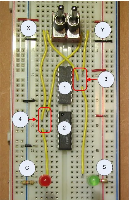
Figure 10-10: ALU Implementation ... 113
I
Forward
This text is designed provide an overview of the basic digital integrated circuits (ICs) that make up the Central Processing Unit (CPU) of a computer. The coverage of the material is at a sufficiently deep level that the text could be used as a supplemental text for a class in Computer Organization, but the material should be easily understandable by a hobbyist who wants a better understanding of how a computer works.
I.1
Why this book?
This book is designed to address three issues. The first is that textbooks are far too expensive. As having completed my 4th book shows, I understand the large amount of effort that goes into writing, editing, producing, and distributing these books. But the work involved no way justifies the exorbitant prices that are charged, and the resultant extravagant lengths people go to in order to avoid paying those prices. It all plays into a hyper-materialistic capitalism that can only eventually fail as it pits consumers against producers, and ignores the overall societal good. I hope by releasing free books (or books with nominal costs) that we can start to have a discussion about the relative merits of this type of unfettered capitalism, and perhaps come up with better, more sustainable market based economic models.
The larger problem with high priced textbooks is the cost alone becomes an impediment to many people who wish to learn the material. Social good is advanced when information can be easily disseminated, shared, and discussed. I view providing this book for free as my contribution to those who want to learn this material.
The second reason for this text is to provide a way to incorporate labs into classes in Computer Organization, particularly online classes. As many colleges and universities moving more classes online, there is a need to translate beneficial methodologies from face-to-face
environments to formats where they are useful in an online environment. One such instructional methodology that is hard to translate is laboratory experiences. A class in Computer
Organization benefits immensely from labs that allow the students to create physical circuits. Labs provide reinforcement for the material covered in class, and the labs represent a fun and exciting way for students to interact with this material. This text is meant to provide a way to incorporate labs into any class on Computer Organization, but especially online classes.
Finally, this text book is written for hobbyists who want to better understand digital circuits and how they work. It is designed for the complete novice, someone who has never seen a
breadboard or IC chip. In fact, it is hoped that people who are afraid they could never get a circuit to work, or understand what it does, will try the exercises in this book and find out just how much talent they have when it comes to understanding and creating circuits.
I.2
Intended Audience
The intended audience is central to what material is covered, the order in which it is covered, and how it is covered. Thus understanding the intended audience will help the reader understand how the book is oriented and how to use it.
in a CPU, and to give a rough idea of how they are used.
The second audience for this text is students who are taking a class in Computer Organization, which is the study of how a CPU works, and the various issues in the design of computers. The text is intended as a lab manual for a Computer Organization class, and in particular targeted at students who are taking this class in an online environment.
Understanding the target audience for this book is important understand how it is written. First the book is written to make understanding and implementing circuits as simple as possible for novices who have little support in implementing these labs. The labs assume no institutional infrastructure or support. No lab space or extra equipment should be needed, and students should be able to complete these labs at home with only the equipment listed in chapter 1.
Second the book is written to address the interests and needs of both the hobbyist and CS students. Both groups have similar but somewhat different levels of interests and the text attempts to address the needs of both groups.
How the text supports these two groups is explained in the next two sections.
I.3
Easy to understand circuit design and implementation
One important characteristic of the target readers for this book is that they will have little or no face-2-face support when implementing the components. Thus the book is written to help maximize the chance for success in implementing the circuits in each chapter. To do this the book does the following:
1) All parts that are needed for all circuits are listed, and can be easily obtained from a number of online sources. There is no need to start a project and reach a point where some extra part is needed.
2) An attempt was made to keep the kits as low cost as possible. This text is free for
download. When the text was written, a complete lab kit (without tools) could be ordered as parts for $20-$25, with $5-$10 extra if wire strippers or pliers are not available. This is a reasonable cost considering many textbooks today can sell for $100 or more.
3) Even simple steps, such as how to strip wires, are covered.
4) An overview of each circuit is given, where the functioning of the circuit and how it is used is explained. Detailed step-by-step instructions with photographs are included with each lab so that the actual wiring of the circuit can be examined.
5) Extensive use is made of a powerful yet easy to use circuit design tool named Logisim. Logisim allows the reader to interact with the circuits and components presented in each chapter to understand how they work, and to modify these circuits to implement
enhanced functionality for the component.
I.4
Material covered in the text
Students using this text as a lab manual are more interested in understanding the details of digital circuits, in particular how to the circuits in their Computer Organization class, and often beyond. Since the students will often be online, success in the projects is also a major goal; as is having fun. Let's face it, actually implementing working, physical objects that turn light bulbs on should be, and is, fun. There is no reason not to have fun while enhancing learning.
This book is designed to engage both types of readers. Chapters 2, 3 4, and 5 of the book are designed to give the reader some basic understanding of Boolean algebra, how a CPU works, and how to build a circuit on a breadboard. The material on Boolean algebra is not rigorous, and a class in Computer Organization would need to supplement this material. The description of a CPU needs to be greatly extended for a class in Computer Organization. But the material in this text is sufficient for the reader to understand enough Boolean algebra to understand basic
circuits, and how they are used in a CPU.
Each subsequent chapter will cover one digital component. The chapter will contain an overview of the component, and a brief description of how it can be used in a CPU. For instructors who desire that students do more with the circuits than what is presented in the chapter, exercises (both in Logisim and with the breadboards) are given at the end of each chapter.
II
Additional text materials
This text can be downloaded from http://cupola.gettysburg.edu/oer/1. Additional materials for the text, including a complete parts list from commercial suppliers with part numbers and prices can be found at http://chuckkann.com.
III
About the second edition
Other than numerous edits to fix errata in the first edition, the main reason for this new release of the text are two fold, and based on the feedback I have received from the first edition.
1. Chapter 2 has been changed to provide a more theoretic background in Boolean algebra for the cases where this book is being used in a course on Computer Organization. This chapter can safely skipped by a hobbyist only interested in how digital circuits work.
2. The chapter 2 in the first edition was intended to give a context for the ICs developed in this text. It seemed out of place and disjointed from the rest of the text. The role of chapter 2 has been moved to chapter 11, which shows the ICs in the context of a working CPU developed by the author.
IV
Using this book in a class on Computer Organization
subtraction, multiplication, and division), and floating point number format.
The next five weeks of the semester are spent covering assembly code. I find this is important for two reasons. First the students should know how their higher level programs are translated into programs which the computer can execute. It allows the students to see all data in a computer as just a binary number, and to understand concepts such as variables and pointers to variables. Second teaching assembly shows the translation by the assembler of the student's program into machine language, and the format of machine code. Understanding how a
program is presented to the hardware is important to the understanding of how the CPU executes the program.
This leaves the last 5 weeks of a semester for actually studying the data path which defines the CPU.
In this type of semester, I do not cover the digital components in this book as a single entity. Chapters 1, 2, and 3 are assigned the first week, and each subsequent chapter assigned each subsequent week. A short overview of each circuit is provided in class, but the students are largely left on their own to do the problems associated with the circuit. By the eighth week, all of the circuits have been covered and the students are ready to begin studying the data path of the CPU. The digital circuits that have been covered in this text form the basis for the
components in the CPU.
A sample 15-week schedule follows. Note that the assignments from this text are the second topic in each week. The first assignment each week represent material used in covering Computer Organization using a MIPS programming text.
Week Topic Circuit Assignment
1 1. Review: Boolean Algebra, Binary Arithmetic
2 1. Floating Point Numbers
2. Basic circuits Due: Chapter 3: Exercise 1 Chapter 4: Exercises 3, 4A, 5, 6
3 1. Introduction to MIPS assembly: Hello World Program
2. Associative operators
Chapter 5: Exercises 1 & 2. Implement the circuit for one type of gate only (your choice)
4 1. MIPS operators
2. Adders Chapter 6: Exercises 2 & 3
5 1. Non-reentrant subprograms, accessing
2. Decoders
6 1. Program Control Structures (branches and loops)
2. Multiplexers
Chapter 8: Exercises 1, 2, 3 & 4
7 1. Reentrant subprograms and program stack
2. Latches and flip-flops Chapter 9: Exercise 1
8 1. Arrays
2. State machines Chapter 10: Exercises 2, 3, &4
9 1. Multiplication and Division circuits, Parallel Adders
10 1. MIPS data path
11 1. Pipelining
12 1. Pipelining (continued)
13 1. High performance memory or concurrency
14 1. I/O or other topics
1.1 Introduction
This chapter provides an overview of the entire text, and what the reader can expect to learn. It also provides a listing of all materials needed to implement the circuits covered in this text.
1.2 Computers and magic
While most would not admit it, people believe that computers actually obey the laws of magic. Computers do such wild and miraculous things that somehow we all believe computers are not really machines at all, but there is something very strange and magical which must go on inside of a computer. Computers seem to do things which are beyond the physical laws of nature. And the growth in the capability of the devices which we use every day, which are small and simple to use yet so amazing in what they can do, reinforces this idea that computers are indeed magic.
In reality, we know computers are simply machines. The first machine ever designed that had all the functionality of a modern computer, the analytical engine, was designed by Charles Babbage in 1838. The analytical engine was to be purely mechanical and designed to run on steam. While it was never implemented, it is a perfectly workable design, and incorporates all the necessary functionality of a modern computer.
The analytical engine shows that computers can be understood in purely mechanical terms. To aid in understanding computers, this text will look at the heart of all computers, the Central Processing Unit (CPU). The first step in understanding computer is to understand a CPU.
A CPU is entirely made up of wires and logic components called gates. These gates are very, very tiny, and very, very fast, but they are just electronic circuits which perform simple
operations. The only operations these gates need to provide are the Boolean AND, OR, and NOT operators, which will be explained in Chapter 4. More surprisingly, AND, OR and NOT
functions are more than what is needed. All of the logic in a computer can be implemented using only one type of gate, the Not-AND, or NAND, gate. Thus a computer is simply a collection of these wires and gates, and can be completely explained as a mechanical device using only one type of computational element, the NAND gate. This really is almost as amazing as computers being made of magic, but much more useful.
To simplify the CPU, collections of AND, OR and NOT gates are organized into digital
components (called Integrated Circuits, or ICs) which are used to build the CPU. These digital ICs are called multiplexors, decoders, flip-flops (registers) and Arithmetic Logic Units (ALUs). Some of these components, such as the ALU, are made up of other digital components, such as adders, subtracters, comparators, and circuits to do other types of calculations. This book will cover these digital ICs, explaining how they are used in a CPU, showing how these digital components are made using simple gates, and actually implementing the circuits on a breadboard using IC chips.
1.3 Reading this text
This textbook is intended for multiple audiences. Chapter 2 of this text is an overview of Boolean algebra and included largely for when the text is use in classes covering digital circuit design. Chapter 2 is not necessary to the understanding of the rest of the book, and can be safely skipped by someone using this text as a lab manual. I would recommend that a hobbyist using this book for bread board project skip Chapter 2 altogether.
Chapter 11 is an implementation of a CPU in Logisim, and shows how a CPU can be designed using only wires, gates, and the ICs that are covered in this text. The implementation is a real CPU which can be programmed, producing input and output. However even this simple CPU is too complex to implement in a Breadboard.
Chapters 3 to 10 are the chapters which implement the projects. These chapters are the important chapters for someone interested in implementing the ICs used in a CPU.
1.4 Materials Needed
This section will outline the materials you will need for the rest of the book. There are two types of materials you will need. The first will be a software program called Logisim, and the second will be physical parts needed to implement the circuits on a breadboard.
1.4.1 Logisim
Logisim is a tool which is used to describe the circuits found in this book. Logisim is free and easy to use, and can be found at http://ozark.hendrix.edu/~burch/logisim/. There is a download link at that site, as well as tutorials and videos which can help you get started.
All circuits in this book are implemented in Logisim, and can be found at
http://www.chuckkann.com/
1.4.2 Hardware
The following is a complete list of hardware that is needed to implement the basic circuits in the text. It is broken down into 3 sections; chips, tools, and miscellaneous parts. For a complete list of parts with part numbers from various retailers, please go to http://www.chuckkann.com.
When buying the hardware, users will often have some of the needed material already on hand. Things like wire stripper, needle-nose pliers, and a small flat-blade screw driver are common items that many people will have readily available. Other items like wire or 9 volt batteries are often available from other uses. If you already own some of the parts or equipment listed below, there is no need to buy them again.
Chips
Except for the 7805 voltage regulator, all of the chips are standard 7400 series chips. For more information about 7400 series logic chips, see http://en.wikipedia.org/wiki/7400_series. A complete list of 7400 series chips can be found at
http://en.wikipedia.org/wiki/List_of_7400_series_integrated_circuits.
where
• 74: indicates the chip is a 7400 series chip
• ttt: the type of logic used. In this text, the following are valid: o blank - transitor-transitor logic (ttl)
o HC - high speed CMOS
o HCT - high speed CMOS, ttl compatible
• sss: The type of chip. For example: o 7408 is a quad 2-input AND gate chip o 7432 is a quad 2-input OR gate chip
• n: Indicates the packaging of the chip. Only type n is used in this text. For most of the 7400 series chips below, ttl, HC, and HCT chips can be considered
interchangeable in the circuits in this text1. So for a 7408 quad 2-input AND gate chip, the following chips would all be valid:
7408N, 74HC08N, 74HCT08N
However the following chips could not be used:
7408D - Any chip designated D is a surface mounted chip, and will not work with the breadboard. Other types of packaging might be encountered, and should be assumed not to be compatible.
74LS08N - There are numerous technologies used to implement 7400 components. For this text, only ttl, HC, and HCT types of chips are recommended. Some type of chips (ACT, BCT, FCT, etc) would probably work, and others (LS, ALVC, etc) will definitely not work. For readers interested in a more detailed discussion of the chip technology, please refer to the Wikipedia page referenced above.
To simplify the process of obtaining the correct chips, a web site is maintained at
www.chuckkann.com/books/DigitalCircuits/kits.html. It lists a number of retailers who sell these chips, and the retailers part numbers for each chip.
A complete list of follows.
7805 5V voltage regulator 1
7400 quad 2-input NAND gate 1 7402 quad 2-input NOR gate 1 7404 hex Inverter (NOT gate) 1 7408 quad 2-input AND gate 2 7414 hex Schmitt Trigger Inverter (NOT gate) 1 7432 quad 2-input OR gate 1 7474 dual D positive edge triggered flip-flop 1 7486 quad 2-input XOR gate 1
74139 dual 2-line to 4-line decoder 1 74153 dual 4-to-1 Multiplexor 1
Important Note: In this text all chips will be referred to using their generic numbers. So while the circuits in the text will generally use a 74HCT08N chip, the text will refer to the chip as a 7408 chip.
Tools
A few tools are useful to implement the labs in this text. The wire strippers are the only required tool, but needle nose pliers are very handy when doing wiring, and a flat blade screw driver makes it much easier to pry chips from the board safely. These tools are often in toolboxes that the reader might already have. If the reader does not have one or more of these tools, they should be obtained.
wire stripper 1
needle nose pliers 1
small bladed screw driver 1
Miscellaneous
A number of miscellaneous parts are needed to implement the circuits in this text. The number of type of these parts is limited specifically to keep the cost of the kits to a minimum. For example, the labs in the text use 4 colors of wire for clarity: red, black, yellow, and green. The kits below only include black wire. The reader can obtain multiple colors of wire if they desire, but the circuits can be implemented using a single color wire.
Be careful of substitutions. For example, a 400 point solderless breadboard is cheaper than the 830 point solderless breadboard which is recommended, and a thrifty reader might be tempted to substitute the smaller board since it looks very similar. However several of the circuits in this text will not fit on the 400 point version.
Wire, black 1 25 foot spool
830 point solderless breadboard 1
9V battery snap 1
9V battery 1
toggle switches 4
red LED 3
green LED 3
1k resistor 1 package of 10
0.1µf capacitor 1 package of 10
0.22µf capacitor 1
mini push button switch (tactile button switch) 1
1.5 Some notes
output LED. Green wires are used for wires which recycle backwards towards the battery (the use of green wires will become clearer when the latch and counter circuits are implemented). The only reason these colors were chosen is to enhance the readability of the circuits for the text. The standard material for the lab kit only recommends purchasing black wire. The color of the wire is inconsequential to the working of the circuit, though using only black wire means your circuits will appear slightly different from the ones in the text, and be harder to read.
Be careful when doing the labs: The exercises in this book require the reader to strip wire and to use simple logic chips. While a young person could do the exercises in this book, it is intended for an adult audience or at least adult supervision. The parts are small, pointy and sharp, and care should be used when handling them. Clipping and stripping wires can result in small pieces of plastic and metal becoming airborne. The components used in these circuits can become very hot, especially if installed backwards. While there is nothing inherently dangerous in working with the circuits, care should be used. Safety glasses are recommended, and if any chip or part of the circuit become hot, quickly remove the power by disconnecting the battery. Do not touch any hot chips or other components, and wait for chips or other components to cool before handling them.
1.6 Conclusion
2.1 Introduction
This chapter introduces the necessary Boolean algebra for understanding circuits. It covers truth tables, Disjunctive Normal Form (DNF) for Boolean functions, Boolean relationships, how to use Boolean Algebra to manipulate and reduce Boolean functions, and how to use Karnaugh maps to minimize Boolean functions.
While the material in this chapter can be understood by someone with a good understanding of algebra, it can be a bit esoteric and is not needed to understand the rest of the textbook. This chapter can be safely skipped by someone using this book as a lab manual. I would suggest that this chapter be skipped by hobbyists using this textbook for bread boarding projects.
2.2 A Universal Set of Boolean Operations
When thinking about Boolean algebra, it is important to realize that Boolean values are binary, so any Boolean variable is limited to two values. Often these values will be True or False, but in reality any binary values can be used. In this textbook, the value 0 will be used for False, and 1 for True. The reason for using 0 and 1 is that it is a more natural and useful way to represent these values in an engineering context, which will hopefully become apparent to the reader as they continue their study of computer organization.
To be useful some minimum set of operations which can be used to manipulate those Boolean variables. For Boolean algebra this minimum set of operations will include just 3 operations, they are AND, OR, and NOT. The AND and OR operations are binary operations (operations that take two operands), and the NOT is a unary operation (operation that takes one operand). These operations will be defined formally using truth tables in the next section. For now they will be defined informally as follows:
• the AND operator is f(A,B), where f(A,B) is 1 (true) where A, B are both 1 (true) otherwise it is 0 (false).
• the OR operator is f(A,B), where f(A,B) is 1 (true) is A or B or both A and B are 1(true), otherwise it is 0 (false).
• the NOT operator is f(A), where f(A) is 1 (true) if A is 0 (false), and f(A) is 0 (false) if a is 1 (true).
This leads to a question as to why these three, and only these three, operations are chosen. The answer is that these three operations are universal Boolean operations. In this context, universal means that any Boolean function can be reduced to combinations of these three operations. Therefore, there is never a need to define any other Boolean operations to calculate a Boolean function. Other useful Boolean operations will be introduced in this textbook, but realize that these operations can be reduced to simply AND, OR, and NOT operations2. The proof of this will be left to the exercises at the end of this chapter.
2 This result, and AND, OR, and NOT are Universal over Boolean functions is even more amazing when it is realized
In this textbook, the AND operation will be written using the multiplication sign, "*", and the result call a product; the OR operation will be written using the "+" sign, and will be called a sum; the NOT operation will be shown by following the variable with a single "'" mark, e.g. A' is NOT-A. Note also that the "*" symbol can be dropped as in standard algebra, so "A*B" can also be written simply as "AB".
2.3 Truth Tables
Boolean functions are functions that perform operations on sets of Boolean variables. For example, a Boolean function f, which takes 2 input values A and B, would produce an output value, f(A,B). The input values A and B are binary, as is the output value f(A,B). It is possible to completely characterize the function f(A,B) by enumerating all the possible input
combinations and A and B (00, 01, 10, 11), and specifying the output f(A,B) for each input combination.
A truth table is standard way to represent a Boolean function which enumerates all the possible outputs of that function. So assume f(A,B) is the AND operator. The truth table for this
operation is:
Input Output
A B AND
0 0 0
0 1 0
1 0 0
1 1 1
Table 2-1: AND truth table
More than one function can be represented in a truth table. A truth table that represents two functions, AND and OR, would be the following:
Input Output
A B AND OR
0 0 0 0
0 1 0 1
1 0 0 1
1 1 1 1
Table 2-2: AND and OR truth table
All Boolean functions can be represented using truth tables (the proof for this is left for the exercises at the end of this section), though the size could become quite large, or possibly
Input Output
A B C f1(A,B,C) f2(A,B,C)
0 0 0 0 0
0 0 1 0 1
0 1 0 0 0
0 1 1 0 1
1 0 0 1 0
1 0 1 1 1
1 1 0 1 0
1 1 1 1 1
Table 2-3: Truth table for f1(A,B,C) and f2(A,B,C)
2.4 Disjunctive Normal Form(DNF)
Disjunctive Normal Form (DNF) is a standard way to write Boolean functions. It can be
described as a sum or products, and an OR and ANDS3. To understand DNF, first the concept of a minterm will be covered.
A minterm is a row in the truth table where the output function for that term is true. For example, in Table 2-3, the function f1(A,B,C) has a minterm when A=1, B=0, and C=0. We can write this minterm a AB'C' (A and not-B and not-C), since A is true, and B and C are both false. Function f1(A,B,C) also has three other minterms, AB'C, ABC', and ABC. So the DNF for the function f1(A,B,C) would be written as:
f1(A,B,C) = AB'C' + AB'C + ABC' + ABC
Note that these minterms are numbers 4, 5, 6, and 74 in the table so a short hand to write the DNF is the following:
f1(A,B,C)= Σ(4,5,6,7) Likewise f2(A,B,C) can be written as:
f2(A,B,C) = A'B'C + A'BC + AB'C + ABC =Σ(1, 3, 5, 7)
Note that any Boolean function can be written in DNF, and DNF requires only 3 types of operations, the AND, OR, and NOT. This is why AND, OR, and NOT are universal. The proof of this is left for the exercises at the end of the chapter.
3 Another way to represent the function is Conjunctive Normal Form (CNF). CNF can be described as a product of
sums, or an AND or ORs. The use of CNF is left to the problems at the end of the chapter.
2.4.1 Boolean Relationships
The next question to be asked is if any Boolean function can be written in DNF, should DNF be used to represent all Boolean functions? The answer to this question comes from the engineering the circuit. At some point, a computer has to implement the Boolean function as a circuit. That circuit will need 1 gate for each operation. And in engineering the circuit, the goal is to
minimize the number of gates needed.
Why should the number of gates be minimized? When a gate is actually included in a circuit, it has 3 bad effects:
• Every gate requires power to operate it. The more gates in the circuit means that power will be needed to operate the computer.
• Since gates require power, they produce heat as a result. More gates mean more heat from the CPU.
• There are always delays in propagating the signal across the gates. The speed of light is very fast, but it is not infinite. The further the electricity has to go to reach the end of the circuit, the longer it takes. So the more gates in the circuit, the slower the CPU. And in modern computers, the speed of light is often the limiting factor in how fast the CPU can cycle, and thus in the speed of the CPU.
Thus the goal in any circuit design is to limit the number of gates in the circuit. For the function f1(A,B,C) in Table 2.3, the number of AND gates is 8, or gates is 3, and not gates is 4, or a total of 15 gates. The question is whether or not the circuit can be implemented in less than 15 gates.
Boolean algebra is the mechanism which is used to answer this question. Boolean algebra is just like traditional algebra in that there are a set of relationships that can be applied to a function to transform it. And those operations are generally somewhat analogous to the operations in traditional algebra, making the transition to Boolean algebra somewhat easier. A list of these relationships is given in table 2.4.
Relationship Rule
No. Relationship Rule No.
x + 0 = x 1 x * 0 = 0 2
x + 1 = 1 3 x * 1 = x 4
x + x = x 5 x * x = x 6
x + x’ = 1 7 x * x’ = 0 8
x + y = y + x 9 xy = yx 10
x + (y + z) = (x + y) + z 11 x(yz) = (xy)z 12 x(y+z) = xy + yz 13 x + yz = (x+y) (x+z) 14 (x+y)’ = x’y’ 15 (xy)’ = x’ + y’ 16
(x’)’ = x 17
All of these relationships except for 15 and 16 should can be easily derived. Relationships 15 and 16 are known as DeMorgan's Laws, and should simply be memorized.
= AB'(C'+C) + AB(C'+C) (rule 13)
= AB'(1) + AB(1) (rule 7)
= AB' + AB (rule 4)
= A(B'+B) (rule 13)
= A(1) (rule 7)
= A (rule 4)
This expression is obviously simpler than the original, and the number of gates needed for this circuit has been reduced from 15 to 0. This reduction was obviously worth the effort.
But how did we know to continue to reduce this expression after "AB' + AB"? This was a significant reduction in itself, form 15 to 4 gates. Since we have now shown that DNF does not necessarily (and often does not) result in a minimum expression, how can we know if a
minimum expression has been reached? That is the topic of the next section of this chapter.
2.5 Karnaugh Maps (K-maps)
Karnaugh Maps (K-maps) are a mechanism for creating minimum Boolean expressions from a truth table. K-maps rely on Gray Codes to create the mapping space, so this chapter will first cover Gray Codes. The chapter will continue with how to set up a map, how to solve a K-map, and how to solve a K-map with don't care conditions.
2.5.1 Gray Codes
Gray codes are simply binary codes where the numbers adjacent numbers differ by a single digit. A single digit number only has a single digit, so it is trivial. Now consider the Gray Code for a two digit numbers. It would be:
00 01 11 10
Table 2-4: 2-digit Gray Codes
In this Gray Code, each number differs from its neighbor by 1 digit. 00->01->11->10->00 (note that the Gray code is circular or wraps around from the bottom to the top). A 3 digit Gray Code can be created by reflecting (like a mirror) the 2 digit Gray Code through a plane, and
Table 2-5: 3-digit Gray Codes
Once again that all values in this table differ from the adjacent values by 1 digit, but in addition the table has been group into collections of 2-bit groupings. For example, the rows 0 and 1 both contain 00x, rows 1 and 2 contain 0x1, rows 2 and 3 contain 10x, rows 3 and 4 contain x10, etc (where x is 0,1). Note that once again the table wraps, so rows 7 and 0 both contain x00.
Gray Codes are useful in partitioning a space to group like elements together, and this property will be used in the next section on K-maps.
2.5.2 2-Variable Karnaugh Maps
A Karnaugh map (or simply K-map) is a mapping of a truth table that partitions the truth table so that elements that have the same values are placed adjacent to each other. It is then easier to see what terms are in common, and to reduce the Boolean expression. For example a 2-variable K-map for a function F(A,B) would be represented as follows, with the values of A in rows and the values of B in the columns.
A/B 0 1
0 A'B' A'B
1 AB' AB
Table 2-6: 2-Variable K-Map
In this table, the rows correspond to A and not-A, and the columns correspond to B and not-B.
Table 2-7: A/A' for 2-variable K-map
equation. For example, consider the following truth table:
Input Output
A B AND
0 0 1
0 1 1
1 0 1
1 1 0
Table 2-9: Truth Table for 2-variable K-map problem.
This truth table maps to the following K-map. In this K-map groups of 2n adjacent items are found, which for a 2-variable K-map can only be groups of 4, 2 and 1. In this map there are 2 groups of 2, as shown below.
Table 2-10: Solving a 2-variable K-map
The two grouping found correspond to A' and B', so the final equation for this K-map is A'+B'.
Two variable K-maps are trivial, and so not very interesting. The next two section will show how to solve the K-maps for more 3 and 4 variables.
2.5.3 3-Variable Karnaugh Maps
3-variable K-maps correspond to Boolean functions of the form f(A, B, C). The K-maps again allow a truth table to be mapped so that rows that differ by 1 or 2 values are placed next to each other. To do this, the Gray Codes that were introduced earlier are used. Note how the values for variables B and C are numbered as Gray Codes in the 3-variable K-map table.
A/BC 00 01 11 10 0 A'B'C' A'B'C A'BC A'BC' 1 AB'C' AB'C ABC A'BC'
Note that once again this number has resulted in regions in the K-map where the variables differ by 1 digit, as shown below. Note that the region C' wraps around the table.
Table 2-12: A/A' region of a 3-variable K-map
Table 2-13: B/B' region of a 3-variable K-map
Table 2-14: C/C' region of a 3-variable K-map
To use the K-map to solve 3 variable functions, once again groupings of 2n are found, which for a 3-variable K-map are 8, 4, 2, and 1. The larger the grouping, the fewer the terms, so groupings of 8 are chosen over groupings of 4, groupings of 4 are chosen over groupings of 2, and
groupings of 2 are chosen over groupings of 1.
The following is an example of how to use a K-map to solve a Boolean expression. Consider a function f(A,B,C) has the following truth table:
Input f(A,B,C)
A B C AND
0 0 0 1
0 0 1 0
0 1 0 0
0 1 1 0
1 0 0 1
1 1 1 1
This expression can be represented as the following sum of products.
f(A,B,C) = Σ(0, 4, 5, 6, 7)
The minimum function for this K-map consists of one group of 4 and one group of 2, and
corresponds to the equation f(A,B,C) = A+B'C'. Note the cell AB'C' is used in both equations, which is rule 5 from the Boolean relationship table, X+X = X, and means that any term in the summation can be used more than once in minimizing the circuit.
To show that the final equation corresponds to the initial truth table, algebra will be used to reduce the expression from DNF to the final form.
f(A,B,C) = Σ(0, 4, 5, 6, 7)
= A'B'C' + AB'C' + AB'C + ABC' + ABC
= A'B'C' + AB'C' + AB'C' + AB'C + ABC' + ABC (rule 5) = (A+A') B'C' + (AB' + AB)(C+C') (rule 13)
= (1) (B'C') + (AB' + AB) (1) (rule 7) = B'C' + AB'+ AB (rule 4)
= (B'C') + A(B'+B) (rule 13) = (B'C') + A(1) (rule 7) = (B'C') + A (rule 4)
2.5.4 4-Variable Karnaugh Maps
While K-maps larger than 4 variables exist, they require more than 2 dimensions and are thus hard to solve by hand, though there are algorithmic ways to do this and there are many programs online that can solve them. This text is only interested in presenting the concept of K-maps and how they are solved, so it will end with presenting 4-Varable K-maps.
AB/CD 00 01 11 10 00 A'B'C'D’ A'B'C’D A'B’CD A'B’CD’ 01 A’BC’D’ A’BC’D A’BCD A'BC'D’ 11 ABC’D’ ABC’D ABCD ABCD’ 10 AB’C’D’ AB’C’D AB’CD AB’CD’
Note that once again this number has resulted in regions in the K-map where the variables differ by 1 digit, as shown below. Note that the regions B' and D’ wrap around the table.
To use the K-map to solve 3 variable functions, once again groupings of 2n are found, which for a 4-Variable K-map are 16., 8, 4, 2, and 1. The larger the grouping, the fewer the terms, so groupings of 16 are chosen over groupings of 8, groupings of 8 are chosen over groupings of 4, groupings of 4 are chosen over groupings of 2, and groupings of 2 are chosen over groupings of 1.
The following is an example of how to use a K-map to solve a Boolean expression. Consider a function f(A,B,C) has the following truth table:
Input f(A,B,C)
A B C D AND
0 0 0 0 1
0 0 0 1 0
0 0 1 0 0
0 1 0 1 1
0 1 1 0 1
0 1 1 1 1
1 0 0 0 1
1 0 0 1 0
1 0 1 0 0
1 0 1 1 0
1 1 0 0 1
1 1 0 1 1
1 1 1 0 1
1 1 1 1 1
This expression can be represented as the following sum of products.
f(A,B,C) = Σ(0, 4, 5, 6, 7, 8, 12, 13, 14, 15)
To show that the final equation corresponds to the initial truth table, Boolean algebra can be used. The derivation of the final equation from the DNF is left as an exercise.
2.5.5 Don’t care conditions
Sometimes when specifying an equation there are a number of situations where the input is not used. If the input is not used, then any value (0 or 1) can be used, and these are called don’t care
conditions. For example, consider a 7-segment display which is used for many time clocks for sporting events. The display consists of 7 segments that are used to display the 10 decimal numbers 0..9. A 7-segment display along with the names for each segment (A..G) is shown below.
Each digit 0-9 will lights 1 or more segments to create the number. For example the digit 0 would light segments A,B,C,D,E,F; the number 1 would light segments B,C; the number 2 would light segments A,B,D,E,G; etc. Therefore, there will be 7 Boolean functions, one for each
segment.
Next, knowing that 10 digits can be represented using a minimum of 4 bits, a truth table can be created where the input 4 digits represent the decimal number, and a truth table developed for each of the 7 segments making up the number. When doing this, note that input values for the truth table must always be between 0-9, so there are 6 values (10-15) that are not used, so those rows in the table are never accessed. The values for the segments for those rows are don’t cares
because they are never used; the component does not use those values, so it does not care how they are set. This gives the result for the 7-segment display truth table, where X=don’t care, which is shown below.
Input Output
A B C D A B C D E F G
0 0 0 0 1 1 1 1 1 1 0
0 0 0 1 0 1 1 0 0 0 0
0 1 0 0 0 1 1 0 0 1 1
0 1 0 1 1 0 1 1 0 1 1
0 1 1 0 1 0 1 1 1 1 1
0 1 1 1 1 1 1 0 0 0 0
1 0 0 0 1 1 1 1 1 1 1
1 0 0 1 1 1 1 0 0 1 1
1 0 1 0 X X X X X X X
1 0 1 1 X X X X X X X
1 1 0 0 X X X X X X X
1 1 0 1 X X X X X X X
1 1 1 0 X X X X X X X
1 1 1 1 X X X X X X X
The K-map for each segment now can be evaluated to give the corresponding minimum Boolean expression. The don’t cares (Xs) in the map are important because we can assume they are 1 when they help us minimize an expression, and assume they are 0 otherwise. In short, we can use them to create larger groupings, but they do not have to be used.
The K-map for segment A is the following:
The result is two groups of 8 (in red and purple) corresponding to A and B, and two groups of 4, one (in black) corresponding to BD, and one (in yellow, crossing the 4 corners of the map) corresponding to B'C', resulting in the following equation for segment A,
fA(A,B,C,D) = A + C + BD + B'D'
2.6 Conclusion
Boolean algebra, or functions where the values are binary or two digit values, is the basis for the circuits that will be presented in this text. Boolean functions can always be represented in a truth table, and then translated directly into DNF. Thus any Boolean function can be written using only AND, OR, and NOT operations.
To instantiate these functions into hardware for a computer, circuits will be used. For a number of reasons, including making the circuit faster and decreasing the amount of electricity used and the amount of heat generated, it is of interest to designers to make the circuits as small as
It is difficult to know if a circuit has been reduced to a minimum using just DNF, so the concept of a K-map was introduced which is a mechanical way to ensure minimum circuits.
2.7 Exercises
1. DeMorgan’s Law:
a. Show that DeMorgan’s Law is correct for two variables, (A’B’)’ = A+B by using a truth table.
b. Does DeMorgan’s Law hold for 3 variables? What about 4 variables?
2. Simplify the following Boolean expressions using Boolean algebra
a. A + AB b. A + A’B c. AB’C’ + ABC’
d. AC + AC’ + A’B + A’B’
3. The operations AND, OR, and NOT are universal in that any Boolean function can be implemented using just these three gates.
a. Prove by construction that the NAND gate is universal by creating AND, OR, and NOT gates using only the NAND gate.
b. Prove by construction that the NOR gate is also universal.
c. Why are the AND and OR gate not universal? (e.g. what simple operation cannot be created with just an AND or OR gate?)
4. For inputs A and B, show how to use an XOR gate to create a NOT gate if B is 1, and a buffer if B is 0.
a. Give the DNF equation for the table. b. Minimize the equation using a K-map.
c. Show that the DNF is equivalent to the minimum representation using Boolean algebra.
A B C F(A,B,C)
0 0 0 0
0 0 1 1
0 1 0 1
0 1 1 0
1 0 0 0
1 0 1 1
1 1 0 1
1 1 1 0
7. For the following truth table
a. Give the DNF equation for the table. b. Minimize the equation using a K-map.
c. Show that the DNF is equivalent to the minimum representation using Boolean algebra.
A B C F(A,B,C)
0 0 0 1
0 0 1 1
0 1 0 1
0 1 1 1
1 0 0 0
1 0 1 1
1 1 0 0
1 1 1 1
8. For the following truth table
c. Show that the DNF is equivalent to the minimum representation using Boolean algebra.
A B C F(A,B,C)
0 0 0 1
0 0 1 0
0 1 0 0
0 1 1 1
1 0 0 1
1 0 1 0
1 1 0 0
1 1 1 1
3.1 Introduction
There is an old adage, “A journey of 1000 miles begins with the first step”. The hardest part of any project is getting started. I had taught Computer Organization for years but had always used
virtual circuits to describe the components presented in this text. That meant using pictures, drawings, and eventually tools such as Logisim. Though I knew the circuits in this book, I was afraid to actually touch the hardware. From my conversations with others, this is not an
uncommon feeling even among computer scientists. Like so many people in so much of life, I was afraid of the beginning.
The beginning, when all the fears about the project are apparent. Do I really know enough to do the project? Will it take a lot longer than I think? What happens if I hit a problem that I cannot solve? Too often these fears take over, and useful projects just fail to get started. But once the project is started, the unknowns become known and can be dealt with. The complexity becomes manageable. Incremental progress can be achieved, and each success builds on the last. The trick is to start very simple, and to allow the complexity to evolve. This is the approach of this text.
This text starts as simply as possible. To begin studying circuits, the first step is to understand that digital circuits take electricity into the circuit, and convert it to an output. In our case, the input will always be a switch, and output will always a LED light. So the first project is a circuit which has a switch which turns on a light.
3.2 Logisim circuit to turn on a light
In this text, all circuits are first created in Logisim to allow the reader to see the logic
implemented by the circuit. This is important for a number of reasons. First, it is much easier to build the circuit in Logisim. No wires need to be cut and stripped, and there are no physical problems like loose connections or other problems to debug. The circuit is virtual and it always behaves as it is coded.
Second, Logisim will represent the circuit as a series of logic gates, which closely represent the Boolean expressions used to create the circuit. When the circuit is implemented using the breadboard and chips, and all the chips look the same so visualizing the circuit is difficult. Logisim makes it easier to understand the circuit, and then to translate it into hardware.
Third, implementing the circuit requires as much concentration on the pin configurations on the chips as the actual gates that are used to implement the logic. Using Logisim allows the reader to understand the logic of the circuit without worrying about extraneous implementation details.
Fourth circuits in Logisim are easier to modify, so problems in implementing the circuit can be more quickly addressed and fixed. Different types of designs for the circuits, inputs to the circuits, etc., can be tried in a much more forgiving environment.
Finally, the circuits which are implemented are more easily saved and shared using Logisim. Most of the circuits in this book will have a Logisim implementation which can be downloaded from http://chuckkann.com/
turns a light on/off. The following list is a step-by-step guide to creating this circuit in Logisim. If you are new to Logisim, you might want to start with the tutorials found at the Logisim site.
Figure 3-1: Logisim circuit to turn on light.
1. Make sure the arrow icon is selected.
2. Select the input pin and place it on the board. 3. Select an output pin, and place it on the board,
4. Connect the right side of the input pin to the left side of the output pin by holding the right mouse button and drawing a line from the input pin to the output pin.
5. The circuit is now complete. Select the hand icon to run the circuit.
6. Clicking on the input pin changes its value from 0 to 1 and back. Since it is directly connected to the output pin, you will also change the output pin.
This circuit will now be implemented in using a breadboard, resistor, 9-volt battery, switch, and led light.
3.3 Implementing the switch circuit to turn on a light
3.3.1 The breadboard
This section describes the breadboard in your lab kits. For more information about breadboards please see the following link:
http://en.wikipedia.org/wiki/Breadboard
The following is a picture of a typical breadboard:
Figure 3-2: Typical breadboard
On the breadboard there are two long strips, called rails, running along the side. The red rail is normally connected to a positive (+5 volts) power supply, and the blue rail is normally connected to ground (0 volts). Note that rails must be connected to a battery or other power source to power them.
There are a number of 10 hole rows in the board, separated by a center empty column. In a row, groups of 5 holes on each side of the empty column are connected. There is no connection between the rows.
This wiring of the breadboard is shown in the Figure 3-3. For the positive and ground rails a wire runs the length of the board which connects the holes in the positive and negative rails. Note that the rails on opposite sides of the breadboard are not connected. Powering one side of the rails does not power both sides, and the rails must be connected to fully power the board. This will be done as part of the circuit created in this chapter.
Figure 3-3: Breadboard layout
This breadboard layout also shows that the groups of 5 holes in each row are also connected, though the top and bottom groups of 5 holes are not. Normally the holes in these groups of 5 on the two sides of the board will be kept separate. This will make sense when chips are installed and used.
The groups of five holes are numbered 1 to 60 on each side of the breadboard. Each group of five holes are wired together, so two wires which are placed in holes in the same group on a row are connected. This will be used to wire the circuits.
3.3.2 Stripping wires
off about 1/4 to 1/2 an inch of insulation. The holes in the breadboard will grab the wires when they are placed inside and make a good contact. If you strip too little insulation off of the wire the connection to the breadboard will probably be poor, and your circuits will not work. If you strip too much insulation off, the circuit will have the possibility of short circuiting. So strip enough insulation so that the wires are grabbed in the hole, but not too much more.
Figure 3-4: Wire strippers
Figure 3-5: A stripped wire
3.3.3 Powering the Circuit
You are now ready to implement the circuit. The steps in creating the circuit will be as follows.
1. Power will be provided to the breadboard.
2. A switch will be inserted into the breadboard.
3. The output from the switch will be sent to the LED, which will complete the circuit.
The first step is to provide power to the breadboard. Pictures of how to power the breadboard are shown in the Figure 3-7and Figure 3-9. These figures contains numbers corresponding to the step-by-step instructions below. As was mentioned earlier, wires in this circuit that always carry a positive voltage are red, ground wires are black, and wires that can take on either value are
yellow.
1) Find the 7805 voltage regulator (shown in Figure 3.6). The 7805 voltage regulator will take the input of 9 volts from the battery and convert it to 5 volts needed by the chips which will be used in the circuit5. Place the 7805 voltage regulator so that it straddles rows 1, 2, and 3 on the breadboard as shown in Figure 3-7. The fit may be tight, so be careful to push it in gently so as to not bend the legs.
2) The input to pin 1 (the pin in row 1 of the breadboard) of the 7805 is the positive 9 volts from the battery. In the figure a red wire is used to indicate this is wire is always connected to positive input. Connect a wire to any hole on the first row, leaving one end not connected to anything. This will be connected to the positive lead of the battery when the breadboard is powered. To test if this is correct, connect the long leg of an led to the positive output of the 7805 regulator, and the short end to the ground, as shown in Figure 3-6. Make sure the battery is new and strong, or you might now get power across the 7805 regulator.
5 Chips used in circuits generally use either 5 volts or 3.3 volts. The chips used in this book will all work with 5
Figure 3-6: 7805 voltage regulator
Figure 3-7: Powering the breadboard
one end not connected to anything. This will be connected to the negative lead of the battery when the breadboard is powered
4) Connect the ground rail of the breadboard to row 2. The ground rail is the blue column which runs down the side of the board. Note that row 2 has three connection, the input ground from the battery, the middle pin on the 7805 chip, and the output wire to the blue ground side rail.
5) The 5 volt output from the 7805 is the pin in row 3. To power the board, connect row 3 to the positive rail of the breadboard. The positive rail is the red column which runs down the side of the board.
6) The left half of the board is ready to be connected to the battery. Put a 9 volt battery in the battery snap, and connect the leads from the battery to red and black wires from steps 3 and 4. (Be sure to connect positive wire to positive input, and negative wire to negative input!) The board should now have power. This can be checked by placing an LED between the positive and negative rails on the board. Note that the LED has two legs, and one is longer than the other, as shown in Figure 3-8. Make sure to place the positive (long) leg in the positive (red) rail, and the short leg in the ground (blue) rail. The light should come on. If it does not, you have a debugging problem. Here are some things to try:
a) Make sure that the battery is connected correctly, positive to positive and negative to negative. If it is not, your 7805 chip will quickly start to become hot. If this happens, disconnect the battery and allow the chip to cool. When the chip is cool, reconnect the battery correctly.
b) Make sure the LED is properly oriented. This simple mistakes often causes confusion, and so when using an LED always make sure to orient it correctly.
c) Make sure the battery and the snap are ok by putting the LED directly into the 9 volt battery clip. If the LED lights, move to step d.
d) Make sure that current is getting to the board correctly. Connect the battery to your positive and negative leads (to power the board) and place the LED between rows 1 and 2 of the board to make sure that you have a good connection with the leads. If the LED lights, move to step e.
e) Make sure you have current coming from the 7805 by connecting the LED between rows 3 and 2. If the LED does not light, something is wrong with the 7805. Check that you have installed it correctly (not backwards for instance).
connected. To connect the right half of the breadboard, go to the last row with the blue and red rails. Run a wire from the left red rail (the outside left rail) to the right red rail (the inside right rail) as shown in Figure 3.7. Do the same for the blue rail. This should power the rails on the right side of the breadboard. You can test that both rails are now powered by using the LED between the blue and red rails on the right side of the breadboard as in step 6 above.
The breadboard is now powered.
3.3.4 Installing the switch
This purpose of this first circuit was to have a switch turn on/off a light. This section will describe how to install the switch. The instructions below refer to Figure 3-11.
0. The switch to be installed is shown in Figure 3-10. There are two nuts and two washers on the switch. These will not be used in the circuits in this book, and make the switch harder to use. Remove them. You may want to save them in case you ever use this switch in a different circuit.
1. To install the switch, insert it across 5 rows of the breadboard. In this picture, the switch is placed across rows 9-13. Only the 1st (row 9), 3rd (row 11), and 5th (row 13) rows will be connected to the switch.
Figure 3-9: Toggle switch
3. The third pin is the negative input. Connect the third pin (row 13) in the switch to the negative rail.
4. The second, or middle, pin is the output. Connect the second or middle pin (row 11) to the final output LED by running a wire from the output (4a) of the switch to the LED (4b) at the bottom of the board.
Figure 3-10: Completed circuit
This type of switch always produces the output from the pin opposite the direction of the switch. When the switch is pointing towards the first (positive) input the output of the switch is negative, and when the switch is pointing towards the third (negative) pin the output is positive. There is also a middle position of the switch. The middle position always is an unknown state, so it could go to either positive or negative. Never check a circuit with the switch in the midd