ABSTRACT
CHAMBERS, JAMES JOSEPH. Reactions for Yttrium Silicate High-k Dielectrics. (Under the direction of Dr. Gregory N. Parsons.)
The continued scaling of metal-oxide-semiconductor-field-effect-transistors (MOSFETs) will require replacing the silicon dioxide gate dielectric with an alternate high dielectric constant (high-k) material. We have exploited the high reactivity of yttrium with both silicon and oxygen to form yttrium silicate high-k dielectrics. Yttrium silicate films with
composition of (Y2O3)x ⋅(SiO2)1-x and x = 0.32 to 0.87 are formed by oxidizing yttrium on
silicon where yttrium reacts concurrently with silicon and oxygen. The competition between silicon and oxygen for yttrium is studied using X-ray photoelectron spectroscopy (XPS) and medium energy ion scattering (MEIS). The initial yttrium thickness mediates the silicon
consumption, and a critical thickness (∼40-80 Å) exists below which silicon is consumed to form yttrium silicate and above which Y2O3 forms without silicon incorporation.
Engineered interfaces modify the silicon consumption, and a nitrided silicon interface results in film with composition close to Y2O3. The silicon consumption also depends on the
oxidation temperature, and oxidation at higher temperature generally results in greater silicon
incorporation with an activation energy of 0.3-0.5 eV. Yttrium silicate films (∼40 Å) formed by oxidation of yttrium on silicon have an amorphous microstructure and an equivalent
silicon dioxide thickness of ∼12 Å with leakage current <1 A/cm2. Yttrium silicate
formation on silicon is also demonstrated using plasma oxidation of yttrium on silicon, reactive sputtering of yttrium and annealing/oxidation of yttrium on thermal SiO2. The
REACTIONS FOR YTTRIUM SILICATE HIGH-K DIELECTRICS
by
JAMES JOSEPH CHAMBERS
A dissertation submitted to the Graduate Faculty of North Carolina State University
in partial fulfillment of the requirements for the Degree of
Doctor of Philosophy
CHEMICAL ENGINEERING
Raleigh 2000
APPROVED BY:
Dr. Gregory N. Parsons
For Amanda,
JAMES JOSEPH CHAMBERS, son of Donald and Marge Chambers, was born on March 21st, 1969. Jim grew up in Munster, Indiana where he played the role of younger brother to
his two older sisters, Dawn and April. His family moved to Parker, Texas just prior to high school. Jim attended school in Plano, Texas and graduated from Plano East Senior High School in 1987. The next stage found Jim at the University of Texas at Austin where he pursued an expansive education. Jim then followed his parents to Albuquerque, New Mexico where he attended the University of New Mexico. A change of venue was again in order, and Jim returned to Texas where he got a dog, Randy, and the dog got him a wife, Amanda. Jim and Amanda were married on March 6, 1993. Jim then took his new bride to luxurious accommodations in Albuquerque, New Mexico to return to school. Jim graduated from the University of New Mexico on May 13th, 1995 with a Bachelor of Science in
ACKNOWLEDGEMENTS
I would like to express my deepest thanks to my parents whose constant support and encouragement was unflappable. I would like to thank my in-laws, Jim and Rebecca Morelock, for supporting Amanda and myself while I dragged their daughter back and forth across the country.
I am grateful to my advisor Dr. Parsons who gave me both the direction and the freedom to thoroughly experience the research process. Dr. Parsons had the wisdom to enable me achieve the most that I could after I came into his office and said that I didn’t have enough to do. I just want to let him know that he gave me more than enough to do.
I want to thank Kit Yeung who has been a great technical teacher, a great life teacher and a great friend. I would never have been able to complete my reactor or my car repairs without his help.
I am indebted to my first mentor, Dr. Joseph Cecchi, for spurring my interest in semiconductors and encouraging me to pursue my Ph.D.
I would like to thank my advisory committee, Dr. Lamb, Dr. Ollis and Dr. Ozturk for their excellent mentoring. A special thanks goes to Dr. Kilpatrick and Dr. Misra for joining my mentoring team on short notice.
Thanks to all the guys at the AIF, especially John Phillips, who helped in obtaining the XP spectra.
Thanks to all the cleanroom people, especially Joan, who’s all right by me.
Although this volume is dedicated to my wife Amanda, I also understand that this work has been a hardship on her as well and she deserves special recognition for all that she has been through. I am grateful for our life together past, present and future. To my eternal beloved.
J.C.
TABLE OF CONTENTS
PAGE
LIST OF TABLES... x
LIST OF FIGURES... xi
1. INTRODUCTION... 1
1.1 HIGH-K DIELECTRICS FOR MOSFET TECHNOLOGY ... 1
1.2 OBJECTIVE... 5
1.3 OVERVIEW OF DISSERTATION... 5
1.4 REFERENCES ... 7
ABSTRACT: PHYSICAL AND ELECTRICAL PROPERTIES OF YTTRIUM SILICATE THIN FILMS... 10
2. PHYSICAL AND ELECTRICAL PROPERTIES OF YTTRIUM SILICATE THIN FILMS... 11
2.1 INTRODUCTION... 11
2.2 EXPERIMENTAL ... 13
2.3 RESULTS AND DISCUSSION ... 14
2.4 CONCLUSIONS ... 16
2.5 ACKNOWLEDGEMENTS... 17
2.6 REFERENCES ... 18
ABSTRACT: PHYSICAL AND ELECTRICAL CHARACTERIZATION OF YTTRIUM SILICATE HIGH-K DIELECTRICS... 28
3. PHYSICAL AND ELECTRICAL CHARACTERIZATION OF YTTRIUM SILICATE HIGH-K DIELECTRICS... 30
3.1 INTRODUCTION... 30
3.2 EXPERIMENTAL ... 34
3.2.1 Sputtering and Surface Pretreatment System... 34
3.2.2 Sample Preparation... 35
3.2.3 Sputter Conditions... 35
3.2.4 Silicidation Conditions ... 36
3.2.5 Thermal Oxidation Conditions... 37
3.2.6 X-ray Photoelectron Spectroscopy... 37
3.2.7 Medium Energy Ion Scattering... 38
3.2.8 Electrical Measurements ... 38
3.2.9 Fourier Transform Infrared Spectroscopy... 39
3.2.10 Atomic Force Microscopy ... 39
3.3 RESULTS AND DISCUSSION... 40
3.3.1 Analysis of Thick (4500 Å) Y-O-Si Films Formed by Oxidation of Yttrium Silicide... 40
3.3.2 Analysis of thin (∼40 Å) Y-O-Si Films Formed by Oxidation of Yttrium on Silicon... 43
3.3.2.1 Physical characterization... 43
3.3.2.2 Electrical characterization... 45
3.3.3 Comparison of Thin Films Formed by Oxidation of Yttrium on Silicon with Thin Films Formed by Oxidation of Yttrium Silicide ... 46
3.3.4 Competition Between Silicide Formation and Oxidation... 51
3.3.5 Analysis of Oxidation Kinetics ... 54
3.4 CONCLUSIONS... 56
3.5 ACKNOWLEDGEMENTS... 57
3.6 REFERENCES... 58
ABSTRACT: YTTRIUM SILICATE FORMATION ON SILICON: EFFECT OF SILICON PRE-OXIDATION AND NITRIDATION ON INTERFACE REACTION KINETICS... 95
4. YTTRIUM SILICATE FORMATION ON SILICON: EFFECT OF SILICON PRE-OXIDATION AND NITRIDATION ON INTERFACE REACTION KINETICS... 97
4.1 INTRODUCTION... 97
4.2 EXPERIMENTAL ... 98
4.3 RESULTS AND DISCUSSION ... 98
4.4 CONCLUSIONS ... 101
4.5 ACKNOWLEDGEMENTS... 102
4.6 REFERENCES ... 103
ABSTRACT: INTERFACE REACTIONS DURING YTTRIUM SILICATE FORMATION ON SILICON... 108
5. INTERFACE REACTIONS DURING YTTRIUM SILICATE FORMATION ON SILICON... 110
5.1 INTRODUCTION... 110
5.2 EXPERIMENTAL ... 112
5.3 RESULTS AND DISCUSSION ... 114
5.3.1 Oxidation of Yttrium on Silicon to Form Y-O-Si Films ... 114
5.3.2 Effect of Silicon Surface Pretreatments on Silicon Incorporation... 118
5.3.3 Consumption of SiO2 by Yttrium... 124
5.4 CONCLUSIONS ... 127
5.5 ACKNOWLEDGEMENTS... 128
ABSTRACT: EFFECT OF OXIDATION TEMPERATURE ON YTTRIUM/SILICON INTERFACE REACTIONS
DURING YTTRIUM SILICATE FORMATION ON Si(100)... 152
6. EFFECT OF OXIDATION TEMPERATURE ON YTTRIUM/SILICON INTERFACE REACTIONS DURING YTTRIUM SILICATE FORMATION ON Si(100)... 154
6.1 INTRODUCTION... 154
6.2 EXPERIMENTAL ... 156
6.3 RESULTS ... 157
6.4 DISCUSSION... 161
6.5 CONCLUSIONS ... 166
6.6 ACKNOWLEDGEMENTS... 167
6.7 REFERENCES ... 168
ABSTRACT: CHEMICAL BONDING AND STRUCTURAL CHARACTERIZATION OF YTTRIUM SILICATE FILMS FORMED BY REMOTE PLASMA OXIDATION OF YTTRIUM ON SILICON ... 179
7. CHEMICAL BONDING AND STRUCTURAL CHARACTERIZATION OF YTTRIUM SILICATE FILMS FORMED BY REMOTE PLASMA OXIDATION OF YTTRIUM ON SILICON... 181
7.1 INTRODUCTION... 181
7.2 EXPERIMENTAL ... 183
7.3 RESULTS ... 184
7.4 DISCUSSION... 188
7.5 CONCLUSIONS ... 192
7.6 ACKNOWLEDGEMENTS... 192
7.7 REFERENCES ... 193
ABSTRACT: END-POINT UNIFORMITY SENSING AND ANALYSIS IN SILICON DIOXIDE PLASMA ETCHING USING IN-SITU MASS SPECTROMETRY ... 204
8. END-POINT UNIFORMITY SENSING AND ANALYSIS IN SILICON DIOXIDE PLASMA ETCHING USING IN-SITU MASS SPECTROMETRY... 206
8.1 INTRODUCTION... 206
8.2 EXPERIMENTAL SYSTEM AND PROCEDURE ... 207
8.2.1 ECR Etching System... 207
8.2.2 Mass Spectrometric Process Sensing System... 208
8.3 RESULTS ... 212
8.3.1 Mass Spectrometric Sensing of Etch Process... 212
8.3.2 Mass Spectrometric End-point Uniformity Sensing... 212
8.4 UNIFORMITY ANALYSIS AND DISCUSSION ... 213
8.4.1 Etch End-point Uniformity Sensing... 213
8.4.2 Etch End-point Uniformity Model ... 215
8.5 CONCLUSIONS ... 220
8.6 ACKNOWLEDGEMENTS... 220
8.7 REFERENCES ... 221
9. SUMMARY... 234
9.1 SUMMARY ... 234
9.1.1 Oxidation of Yttrium Silicide ... 234
9.1.2 Oxidation of Yttrium on Silicon... 234
9.1.3 Yttrium/Silicon Interface Reactions ... 235
9.1.4 Plasma Oxidation of Yttrium on Silicon ... 236
9.1.5 End-point Uniformity Sensing... 237
9.2 SUGGESTIONS FOR FUTURE WORK ... 237
APPENDICES... 238
A. THERMAL OXIDATION OF SPUTTERED YTTRIUM... 239
A.1 TWO-STEP OXIDATION ... 239
A.2 SPUTTER AUGER ELECTRON SPECTRSCOPY ... 241
A.3 ADDITIONAL TEM STUDIES... 243
B. PLASMA OXIDATION... 250
B.1 C-V TESTING OF PLASMA OXIDIZED Y-O-Si FILMS... 250
B.2 REMOTE PLASMA OXIDATION OF TANTALUM ON SILICON... 251
C. REACTIVE SPUTTERING OF YTTRIUM... 253
C.1 ELLIPSOMETRY... 253
C.2 FTIR ... 253
C.3 XPS ... 254
LIST OF TABLES
PAGE
3. PHYSICAL AND ELECTRICAL CHARACTERIZATION OF YTTRIUM SILICATE HIGH-K DIELECTRICS
Table 3.1 Free energy of formation per oxygen atom for metal oxides
and the expected oxidation products of their metal silicides. ... 64
8. END-POINT UNIFORMTIY SENSING AND ANALYSIS IN SILICON DIOXIDE PLASMA ETCHING USING IN SITU MASS SPECTROMETRY
Table 8.1 Assignments and sources for masses shown in Fig. 8.3.
LIST OF FIGURES
PAGE 1. INTRODUCTION
Figure 1.1 Physical thickness versus EOT for SiO2, k=15 and k=80. ... 9
2. PHYSICAL AND ELECTRICAL PROPERTIES OF YTTRIUM SILICATE THIN FILMS Figure 2.1a Schematic depicting crystal structure of Y2Si2O7. ... 19
Figure 2.1b Schematic depicting crystal structure of Y2SiO5... 20
Figure 2.2 Y 3d portion of the XPS spectra for Y-O-Si and Y2O3. ... 21
Figure 2.3 Si 2p portion of the XPS spectra for Y-O-Si and SiO2... 22
Figure 2.4 O 1s portion of the XPS spectrum for Y-O-Si, Y2O3 and SiO2... 23
Figure 2.5a Mid-IR region of the FTIR spectrum for Y-O-Si and SiO2... 24
Figure 2.5b Far-IR region of the FTIR spectrum for Y-O-Si and Y2O3... 25
Figure 2.6 AFM image for Y-O-Si with RMS surface roughness of 8.0 nm. ... 26
Figure 2.7 C-V curve for Y-O-Si with EOT = 5.0 nm... 27
3. PHYSICAL AND ELECTRICAL CHARACTERIZATION OF YTTRIUM SILICATE HIGH-K DIELECTRICS Figure 3.1a Schematic depicting crystal structure of Y2Si2O7. ... 61
Figure 3.1b Schematic depicting crystal structure of Y2SiO5... 62
Figure 3.1c Y2O3-SiO2 phase diagram. ... 63
Figure 3.2 Diagram of system used to sputter yttrium and perform vacuum anneals. ... 65
Figure 3.3a Y 3d region of the photoelectron spectra of Y-O-Si and Y2O3... 66
Figure 3.3c O 1s region of the photoelectron spectra of Y-O-Si,
Y2O3 and SiO2. ... 68
Figure 3.4 Mid (a) and Far (b) IR regions of the FTIR spectrum for Y-O-Si,
Y2O3 and SiO2. ... 69
Figure 3.5a Survey spectrum for Y-O-Si film formed by oxidation of ∼8 Å
of yttrium on silicon at 900 °C. ... 70
Figure 3.5b Y 3d spectrum for Y-O-Si film formed by oxidation of ∼8 Å
of yttrium on silicon at 900 °C. ... 71
Figure 3.5c Si 2p spectrum for Y-O-Si film formed by oxidation of ∼8 Å
of yttrium on silicon at 900 °C. ... 72
Figure 3.5d O 1s spectrum for Y-O-Si film formed by oxidation of ∼8 Å
of yttrium on silicon at 900 °C. ... 73 Figure 3.6 TEM cross-section of a 42 Å Y-O-Si film formed by oxidation
of ∼8 Å of yttrium on silicon at 900 °C. ... 74
Figure 3.7 AFM image of an Y-O-Si film formed by oxidation of ∼8 Å
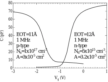
of yttrium on silicon at 900 °C. ... 75 Figure 3.8 Typical C-V curves for thin Y-O-Si films formed by
oxidation of ∼8 Å of yttrium on n- and p-type silicon
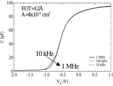
at 900 °C with Al electrodes... 76 Figure 3.9 C-V curves from 10k-1M Hz for a thin Y-O-Si film formed
by oxidation of ∼8 Å of yttrium on n-type silicon at 900 °C
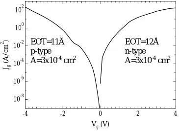
with Al electrode... 77 Figure 3.10 J-V curves for Y-O-Si films on n- and p-type silicon presented
in Fig. 3.8. ... 78
Figure 3.11a Y 3d spectra for 25 Å yttrium films oxidized at 600 °C
and 25 °C. ... 79
Figure 3.11b Si 2p spectra for 25 Å yttrium films oxidized at 600 °C
and 25 °C. ... 80
Figure 3.11c O 1s (c) spectra for 25 Å yttrium films oxidized at 600 °C
Figure 3.12 Si 2p photoelectron spectra for Y-O-Si films formed by
oxidation of yttrium on silicon and yttrium silicide at 900 °C (a)
and 600 °C (b). ... 82 Figure 3.13 Diagram illustrating the processes used to form the films
in Fig. 3.11, 3.12 and 3.14... 83
Figure 3.14a Y 3d spectra for films formed by the oxidation at 600 °C
of yttrium (30 Å) on silicon and yttrium silicide. ... 84
Figure 3.14b Si 2p spectra for films formed by the oxidation at 600 °C
of yttrium (30 Å) on silicon and yttrium silicide. ... 85
Figure 3.14c O 1s spectra for films formed by the oxidation at 600 °C
of yttrium (30 Å) on silicon and yttrium silicide. ... 86
Figure 3.15a Y 3d spectra for ∼8-240 Å yttrium films on silicon oxidized at 900 °C. Initial yttrium coverage <40 Å results in an
Y-O-Si film. ... 87
Figure 3.15b Si 2p spectra for ∼8-240 Å yttrium films on silicon oxidized
at 900 °C. ... 88 Figure 3.15c O 1s spectra for ∼8-240 Å yttrium films on silicon oxidized
at 900 °C. ... 89 Figure 3.16 Diagram illustrating the film structure obtained for thin
and thick initial yttrium coverage. ... 90 Figure 3.17 Si-O/Si area ratio for yttrium films on silicon oxidized at 600 ( )
and 900 °C( ) plotted with thickness data from cross-section TEM images for Y-O-Si films oxidized at 900 °C ( ) and from
ellipsometry for SiO2 films grown at 900 °C ( ). ... 91
Figure 3.18 Cross-sectional TEM image for ∼8 Å yttrium film on silicon
oxidized for 20 minutes at 900 °C... 92
Figure 3.19 Si 2p region for an ∼8 Å yttrium film on silicon oxidized
for 20 minutes at 900 °C... 93
Figure 3.20 Y 3d region for ∼8 Å yttrium films on silicon oxidized
4. YTTRIUM SILICATE FORMATION ON SILICON: EFFECT OF SILICON PRE-OXIDATION AND
NITRIDATION ON INTERFACE REACTION KINETICS
Figure 4.1 Y 3d photoelectron spectra for films formed on a) silicon,
b) silicon oxide, c) nitrided oxide and d) nitrided silicon... 104 Figure 4.2 O 1s photoelectron spectra for films formed on a) silicon,
b) silicon oxide, c) nitrided oxide and d) nitrided silicon... 105 Figure 4.3 Si 2p photoelectron spectra for films formed on a) silicon,
b) silicon oxide, c) nitrided oxide and d) nitrided silicon... 106 Figure 4.4 MEIS energy spectra for films formed on a) silicon
and d) nitrided silicon... 107
5. INTERFACE REACTIONS DURING YTTRIUM SILICATE FORMATION ON SILICON
Figure 5.1a Y 3d region of the XP spectrum for a Y-O-Si film formed by oxidation of an ∼8 Å yttrium film on silicon at 900 °C
for 15 seconds.. ... 131 Figure 5.1b Si 2p region of the XP spectrum for a Y-O-Si film formed
by oxidation of an ∼8 Å yttrium film on silicon at 900 °C
for 15 seconds. ... 132 Figure 5.1c O 1s region of the XP spectrum for a Y-O-Si film formed
by oxidation of an ∼8 Å yttrium film on silicon at 900 °C
for 15 seconds. ... 133 Figure 5.2 MEIS spectrum for a Y-O-Si film formed by oxidation of an
∼8 Å yttrium film on silicon at 900 °C for 15 seconds. ... 134
Figure 5.3a Angle resolved XPS of the Y 3d region for a Y-O-Si film formed by oxidation of a ∼25 Å yttrium film on silicon
at 900 °C for 2 minutes... 135 Figure 5.3b Angle resolved XPS of the Si 2p region for a Y-O-Si film
formed by oxidation of a ∼25 Å yttrium film on silicon
at 900 °C for 2 minutes... 136 Figure 5.3c Angle resolved XPS of the O 1s region for a Y-O-Si film
formed by oxidation of a ∼25 Å yttrium film on silicon
Figure 5.4 Cross-sectional TEM image of a Y-O-Si film formed by oxidation of an ∼8 Å yttrium film on silicon at 900 °C
for 15 seconds. ... 138 Figure 5.5 Typical 1 MHz C-V curve for an Al/Y-O-Si/n-type capacitor... 139
Figure 5.6 Si 2p (a) and N 1s (b) spectra for the silicon surface pretreatments used in this study: (1) clean silicon, (2) plasma oxidized silicon, (3) plasma nitrided-oxidized
silicon, and, (4) plasma nitrided silicon... 140 Figure 5.7a Y 3d regions of the XP spectra for the Y-O-Si films formed
on: (1) clean silicon, (2) plasma oxidized silicon, (3) plasma
nitrided-oxidized silicon, and, (4) plasma nitrided silicon. ... 141 Figure 5.7b Si 2p region of the XP spectra for the Y-O-Si films formed on:
(1) clean silicon, (2) plasma oxidized silicon, (3) plasma
nitrided-oxidized silicon, and, (4) plasma nitrided silicon. ... 142 Figure 5.7c O 1s region of the XP spectra for the Y-O-Si films formed on:
(1) clean silicon, (2) plasma oxidized silicon, (3) plasma
nitrided-oxidized silicon, and, (4) plasma nitrided silicon. ... 143 Figure 5.8 MEIS spectra for the Y-O-Si films formed on: (1) clean silicon,
(2) plasma oxidized silicon, (3) plasma nitrided-oxidized silicon,
and, (4) plasma nitrided silicon. ... 144 Figure 5.9 Calculated MEIS depth profiles for the Y-O-Si films formed
on (1) clean silicon and (4) nitrided silicon. ... 145
Figure 5.10a Y 3d spectra for a 40 Å reference SiO2 and ∼25 Å yttrium films
on 40 Å SiO2 oxidized at 600 and 900 °C for 2 minutes... 146
Figure 5.10b Si 2p spectra for a 40 Å reference SiO2 and ∼25 Å yttrium films
on 40 Å SiO2 oxidized at 600 and 900 °C for 2 minutes... 147
Figure 5.10c O 1s spectra for a 40 Å reference SiO2 and ∼25 Å yttrium films
on 40 Å SiO2 oxidized at 600 and 900 °C for 2 minutes... 148
Figure 5.11a Y 3d spectra for a 40 Å reference SiO2 and a ∼25 Å yttrium film
on 40 Å SiO2 annealed in vacuum at 600 °C for 2 minutes. ... 149
Figure 5.11b Si 2p spectra for a 40 Å reference SiO2 and a ∼25 Å yttrium film
Figure 5.11c O 1s (c) spectra for a 40 Å SiO2 and a ∼25 Å yttrium film
on 40 Å SiO2 annealed in vacuum at 600 °C for 2 minutes. ... 151
6. EFFECT OF OXIDATION TEMPERATURE ON YTTRIUM/SILICON INTERFACE REACTIONS
DURING YTTRIUM SILICATE FORMATION ON Si(100)
Figure 6.1a Y 3d region of the photoelectron spectra for oxidation at
25 to 900 °C of 25 Å yttrium films on silicon... 170 Figure 6.1b Si 2p region of the photoelectron spectra for oxidation at
25 to 900 °C of 25 Å yttrium films on silicon... 171 Figure 6.1c O 1s region of the photoelectron spectra for oxidation at
25 to 900 °C of 25 Å yttrium films on silicon... 172
Figure 6.2 Y 3d angle resolved XPS spectra for take-off angles from 20° to
90° for 25 Å yttrium films on silicon oxidized at 600 and 900 °C. .... 173
Figure 6.3 Si 2p angle resolved XPS spectra for take-off angles from 20° to
90° for 25 Å yttrium films on silicon oxidized at 600 and 900 °C. .... 174
Figure 6.4 O 1s angle resolved XPS spectra for take-off angles from 20° to
90° for 25 Å yttrium films on silicon oxidized at 600 and 900 °C. .... 175 Figure 6.5 MEIS proton energy spectra for 25 Å yttrium films on silicon
oxidized at 600 and 900 °C. ... 176 Figure 6.6 Compilation of the results presented in Figs. 1 and 5. The
Y 3d5/2 ( ) and Si 2p ( ) binding energies, Si-O/Y area
ratio ( ), Si/Y ratio ( ) and thickness (
♦
) are plotted versus
the oxidation temperature. ... 177 Figure 6.7 Arrhenius plot of the Si-O/Si area ratio ( ) and MEIS silicon
fraction times thickness ( ) versus inverse temperature for
7. CHEMICAL BONDING AND STRUCTURAL CHARACTERIZATION OF YTTRIUM SILICATE FILMS FORMED BY REMOTE PLASMA OXIATION OF YTTRIUM ON SILICON
Figure 7.1a Y 3d region of the photoelectron spectra for (1) 30 Å yttrium on silicon remote N2O plasma oxidized for 60 minutes at
100 °C, (2) 30 Å yttrium on silicon remote N2O plasma oxidized
for 60 minutes at 300 °C, and, (3) 30 Å yttrium on silicon remote N2O plasma oxidized for 60 minutes at 100 °C
followed by post-oxidation anneal for 4 hours at
900 °C in 1 atm. N2. ... 194
Figure 7.1b Si 2p region of the photoelectron spectra for (1) 30 Å yttrium on silicon remote N2O plasma oxidized for 60 minutes at
100 °C, (2) 30 Å yttrium on silicon remote N2O plasma oxidized for 60 minutes at 300 °C, and, (3) 30 Å yttrium on silicon remote N2O plasma oxidized for 60 minutes at 100 °C
followed by post-oxidation anneal for 4 hours at
900 °C in 1 atm. N2. ... 195
Figure 7.1c O 1s region of the photoelectron spectra for (1) 30 Å yttrium on silicon remote N2O plasma oxidized for 60 minutes at
100 °C, (2) 30 Å yttrium on silicon remote N2O plasma oxidized
for 60 minutes at 300 °C, and, (3) 30 Å yttrium on silicon remote N2O plasma oxidized for 60 minutes at 100 °C
followed by post-oxidation anneal for 4 hours at
900 °C in 1 atm. N2. ... 196
Figure 7.2.1 Cross-sectional TEM image of a 30 Å yttrium film on silicon
remote N2O plasma oxidized for 60 minutes at 100 °C. ... 197
Figure 7.2.3 Cross-sectional TEM image of a 30 Å yttrium film on silicon remote N2O plasma oxidized for 60 minutes at 100 °C followed
by a post-oxidation anneal for 4 hours at 900 °C in N2... 197
Figure 7.3.1 RHEED image of a 30 Å yttrium film on silicon remote N2O
plasma oxidized for 60 minutes at 100 °C. ... 198 Figure 7.3.2 RHEED image of a 30 Å yttrium film on silicon remote N2O
plasma oxidized for 60 minutes at 300 °C. ... 198 Figure 7.3.3 RHEED image of a 30 Å yttrium film on silicon remote N2O
plasma oxidized for 60 minutes at 100 °C followed by a
Figure 7.4 AFM images for (1) 30 Å yttrium on silicon remote N2O plasma
oxidized for 60 minutes at 100 °C (RMS = 8.9 Å), (2) 30 Å yttrium on silicon remote N2O plasma oxidized for 60 minutes
at 300 °C (RMS = 1.4 Å), and, (3) 30 Å yttrium on silicon remote N2O plasma oxidized for 60 minutes at 100 °C
followed by post-oxidation anneal for 4 hours at 900 °C in
1 atm. N2 (RMS = 1.7 Å)... 200
Figure 7.5 AFM images for 30 Å yttrium on silicon remote N2O plasma
oxidized for zero (a), 5 (b), 10 (c) and 20 minutes (d) at 100 °C. ... 201 Figure 7.6 Results of AFM RMS roughness measurements for 30 Å
yttrium on silicon remote N2O plasma oxidation for
zero, 5, 10, 20 and 60 minutes at 100 °C ( ), remote N2O
plasma oxidized for 60 minutes at 300 °C ( ) and film
post-oxidation annealed for 4 hours at 900 °C in 1 atm. N2 ( )... 202
Figure 7.7 Results of J-V testing of a 30 Å yttrium on silicon remote N2O
plasma oxidation for 60 minutes at 300 °C. ... 203
8. END-POINT UNIFORMTIY SENSING AND ANALYSIS IN SILICON DIOXIDE PLASMA ETCHING USING IN SITU MASS SPECTROMETRY
Figure 8.1 Electron cyclotron resonance plasma reactor used for silicon
dioxide etching. ... 223 Figure 8.2 Schematic of the two stage differentially pump mass spectrometer
system utilized in these investigations. ... 224 Figure 8.3 Real-time intensity signals for the masses monitored in these
investigations. ... 226 Figure 8.4 Real-time CO+ intensity for wafer uniformly (97.7%) covered
by 1000 Å oxide (solid line), 67% thickness uniformity
(50% 1000 Å SiO2 coverage) wafer (dashed line) and 60% thickness
uniformity (75% 1000 Å SiO2 coverage) wafer (dotted line). ... 227 Figure 8.5 Real-time CO+ intensity for uniformity series performed on
uniform oxide films... 228 Figure 8.6 Real-time CO+ intensity for uniformity series performed on
Figure 8.7 Averaged slope of real-time CO+ intensity for 94.7%, 92.1% and
86.2% uniformity versus time... 230
Figure 8.8 Uniformity versus the inverse of the initial slope [s/a.u./1010] for the uniform and non-uniform films (solid points) and first derivative [s-cm3/moles/2.6 X 1012] of the model (solid line)... 231
Figure 8.9 First derivative versus time of COF2 concentration from material balance model. The first derivative at the end-point beginning (t=zo/a) is correlated with the uniformity in Fig. 8.8... 232
Figure 8.10 Average slope of real-time CO+ intensity for the 94.7% uniformity case... 233
APPENDIX A TWO-STEP OXIDATION Figure A.1 C-V curves for one- (a) and two-step (b) oxidation processes. ... 240
Figure A.2 AES surface spectrum (a) and AES depth profile (b) for ∼8 Å yttrium film on silicon oxidized for 15 seconds in 1 atm. air... 242
Figure A.3.1 TEM images for 6 second (a) and 15 second (b) oxidation. ... 244
Figure A.3.2 TEM image for 60 second (c) oxidation. ... 245
Figure A.4.1 TEM images for 1 second (a) and 15 second (b) oxidation. ... 246
Figure A.4.2 TEM images for 1 minute (c) and 2 minute (d) oxidation. ... 247
Figure A.4.3 TEM image for 20 minute (e) oxidation. ... 248
Figure A.5 TEM images for 15 second oxidation taken at different transmission thickness. ... 249
APPENDIX B PLASMA OXIDATION Figure B.1 C-V of Y-O-Si film formed by remote N2O plasma oxidation. ... 250
APPENDIX C REACTIVE SPUTTERING OF YTTRIUM
Figure C.1 Thickness (a) and refractive index (600 nm) (b) from
ellipsometry for reactively sputtered Y-O-Si films. ... 256 Figure C.2 FTIR spectra for reactively sputtered Y-O-Si films. The films
were deposited with a Ar:N2O ratio of 1:2 at a substrate
temperature of 25 °C... 257 Figure C.3 Y 3d, Si 2p and O 1s regions of the XP spectra for Y-O-Si films
deposited by reactive sputtering. ... 258 Figure C.4 C-V characteristic of Y-O-Si film deposited by
CHAPTER 1
INTRODUCTION
1.1 HIGH-K DIELECTRICS FOR MOSFET TECHNOLOGY
Silicon dioxide has been the gate dielectric of choice since 1960 when it was first proposed that thermally grown SiO2 should be used as the gate insulator in
metal-oxide-semiconductor-field-effect-transistors (MOSFETs).1 Research, development and production
over the past four decades have shown SiO2 to exhibit superior low-defect interfacial
properties and to provide excellent passivation of the silicon surface from contamination. The properties of silicon dioxide have been characterized as well as any other dielectric, and SiO2 is entrenched as one of the most basic components in silicon technology. Progress in
silicon integrated circuit technology has been dominated by the reduction in gate length to increase device performance and integration. To keep pace with drive current demands, the silicon dioxide gate dielectric thickness must also scale in accordance with the gate length. In the past, scaling the gate dielectric thickness has simply been handled by a recipe change where either the oxidation time or temperature was decreased to net a thinner dielectric. However, scaling the dielectric thickness has resulted in device degradation in recent years.
As a result of device scaling, boron penetration from the polysilicon gate electrode through the silicon dioxide gate dielectric into the channel region has become a major concern. Boron depletion causes both an increase in the equivalent oxide thickness (EOT) and threshold voltage shifting. However, incorporating nitrogen into the silicon dioxide gate dielectric has been demonstrated to reduce boron penetration, reduce electrically active traps
been explored to achieve the desired nitrogen profiles in the thin silicon dioxide, including furnace annealing, rapid thermal annealing and remote plasma nitridation.3-5 Even though
nitridation has played an important role in device scaling, it is only a near term solution, since the gate dielectric thickness rapidly approaches the quantum tunneling regime where the exponential increase in current with decreasing thickness is one of the more fundamental limits to device scaling.
Since the silicon dioxide thickness is rapidly approaches the quantum tunneling regime, the latest addition to the “show stopper” list is the proposed physical limit of 20-15 Å for the silicon dioxide gate dielectric.6 The physical limit is derived from analysis of the
quantum mechanical tunneling of electrons, which for a change of dielectric thickness of ∼35
to ∼15 Å increases ∼13 orders of magnitude from 10-12 A/cm2 to 10 A/cm2.6 This drastic
increase in leakage current raises severe reliability and power consumption concerns for device operation in this regime, which has prompted interest in the development of alternative high dielectric constant (high-k) materials.
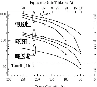
The integration of high-k dielectrics into current MOSFET technology can potentially enable continued device scaling. Since capacitance scales as the dielectric constant over the dielectric thickness, a high-k dielectric should provide sufficient physical thickness to block electron tunneling, while maintaining the specific desired capacitance. When designing a new device technology, this specific capacitance is usually described in terms of an equivalent oxide thickness (EOT). Figure 1.1 illustrates the potential roadblock associated with scaling the silicon dioxide thickness and the potential advantages high-k dielectrics can provide. Figure 1.1 plots the physical thickness versus the device generation and EOT for SiO2 (k = 3.9) and high-k dielectrics with k = 15 and k = 80. The EOT values
Semiconductors (ITRS).7 For each high-k dielectric, three curves are presented where the
high-k is assumed to be on an interfacial SiO2 layer of zero, 7 and 15 Å, where the physical
thickness is calculated using a simple capacitors in series model. The proposed tunneling limit for SiO2 is illustrated in Fig. 1.1 as the dashed line at a physical thickness of 15 Å. It is
clear from Fig. 1.1 that SiO2 will cross the tunneling limit somewhere around the 100-50 nm
device nodes. Therefore, a high-k dielectric will be necessary to achieve the device performance required of a 50 nm device. A high-k material with a dielectric constant of 15 without an interfacial SiO2 layer will enable EOT = 10 Å while remaining above the
tunneling limit. A high-k with a dielectric constant of 80 can afford up to 7 Å of interfacial SiO2 and still achieve EOT = 10 Å while remaining above the proposed tunneling limit.
With these considerations in mind, recent interest in high dielectric constant (high-k) materials currently focuses on the eventual replacement of silicon dioxide.
To replace silicon dioxide as the gate insulator in MOSFET technology, high-k dielectrics must exhibit properties similar to the SiO2/Si system. Any high-k dielectric must
provide low levels of interface defects with interface trap density (Dit) ∼1010 cm-2⋅eV-1 and
fixed charges (Qf) <5x1010 cm-2. High breakdown fields in excess of 10 MeV/cm are also
necessary. The increased physical thickness of a high-k dielectric should limit tunneling current to <1 A/cm2, but the tunneling current is also exponentially dependent on the
barrier height. Therefore, a high-k dielectric should possess a suitably large bandgap and barrier height. However, the bandgap is inversely proportional to the dielectric constant for many high-k dielectrics, consequently the bandgap decreases as the dielectric constant increases.8 The danger exists that the leakage reduction achieved by an increase in the
bandgap should increase the chance of obtaining a suitably large barrier height. The physical properties of any potential high-k dielectric are also crucial, and a covalent amorphous microstructure is advantageous, since grain boundaries may provide high conductivity pathways. The stability between the high-k dielectric and silicon is of paramount importance. Instability of the high-k/Si or polysilicon/high-k interface resulting in excess formation of SiO2 can reduce the effective dielectric constant of the stack and negate the
benefits of the high-k, as illustrated in Fig. 1.1. Integration of a high-k dielectric into the current process flow requires the high-k to remain stable during the particularly strenuous
dopant “drive-in” anneal (∼1000 °C, ∼30s). As of today, no one material has been identified that meets all these requirements.
The most common materials proposed to replace silicon dioxide are the metal oxides, including Ta2O5, TiO2, HfO2, ZrO2, Y2O3, and Al2O3, and the metal silicates,
including Hf, Zr and Y silicates.9-15 The major drawbacks associated with the metal oxides
are: 1) instability on silicon, namely for Ta2O5 and TiO2, resulting in low-k interface layers,12
2) pure metal oxides tend to crystallize at relatively low temperatures (∼200 °C),16 and, 3)
pure metal oxides tend to conduct oxygen, and the oxygen diffusion can lead to oxidation of
the silicon substrate, as well as, oxygen vacancies that act as traps.17 Silicate films may
alleviate some of these problems by combining the high-k advantages of the pure metal oxide with the electrical advantages of SiO2. MOS capacitors using Hf, Zr or Y silicates as
the dielectric have been demonstrated with k∼12.9,15 Furthermore, amorphous
microstructure has been demonstrated for Hf and Zr silicates after annealing at 1050 °C
1.2 OBJECTIVE
Developing an alternate high-k material to replace silicon dioxide as the gate dielectric in MOSFET technology is an arduous undertaking, and the ITRS has set an aggressive timetable for implementation for these materials. Taking into consideration the present knowledge and future needs of high-k dielectrics we have outlined certain goals for this work. The first is to evaluate and develop processes to form yttrium silicate films on silicon. Specifically, we will appraise oxidation of yttrium on silicon, both thermal and plasma, and reactive sputtering of yttrium as methods toward yttrium silicate formation. Next, we must determine of the physical properties of yttrium silicate films on silicon, including their microstructure and local bonding configurations. Another goal is to
demonstrate yttrium silicate films with EOT ≅ 10 Å and leakage current <1 A/cm2. And
finally, we will show the effect of metal-silicon bonds on silicon consumption and interface formation.
1.3 OVERVIEW OF DISSERTATION
This dissertation focuses on the development of yttrium silicate as a high-k replacement for silicon dioxide in MOSFET technology, the physical and electrical properties of yttrium silicate and the role of metal-silicon bonds on silicon incorporation and interface formation. The main approach we use to form yttrium silicate thin films is the thermal oxidation of yttrium metal on silicon. The yttrium silicate forms through a competition for yttrium through reactions with silicon and oxygen. This competition can be mediated by the thickness of the initial yttrium film, the oxidation temperature and through the implementation of engineered interfaces.
SiO2 and Y2O3, evaluate the surface morphology of yttrium silicate and characterize yttrium
silicate MOS capacitors.
In CHAPTER THREE, we discuss the physical and electrical properties of yttrium silicate thin films, compare the film formation by oxidation of yttrium on silicon and by oxidation of yttrium silicide, describe the competition between silicide formation and oxidation, and finally, analyze the oxidation kinetics of yttrium films on silicon.
In CHAPTER FOUR, we demonstrate the ability to control silicon consumption through the use of engineered interfaces.
In CHAPTER FIVE, we further analyze the effect of oxidized silicon and nitrided silicon interface layers on the consumption of silicon during the oxidation of yttrium and we demonstrate the interface reaction between yttrium and SiO2 to form yttrium silicate.
In CHAPTER SIX, we describe the effect of oxidation temperature on silicon consumption and analyze the energetics of silicon incorporation.
In CHAPTER SEVEN, we present the chemical bonding and structural characterization of yttrium silicate thin films formed by the remote N2O plasma oxidation of
yttrium on silicon.
In CHAPTER EIGHT, we present a study on the use of mass spectrometry to sense silicon dioxide etch end point uniformity and propose a model to explain the observed mass spectrometry signal.
In CHAPTER NINE, we summarize the major results of this work.
1.4 REFERENCES
1 M. M. Atalla, U.S. Patent 3,206,670 (1960).
2 H. Hwang, W. Ting, D.-L. Kwong, and J. Lee, IEEE Electron Device Lett. 12
(1991).
3 Y. Wu, H. Niimi, H. Yang, G. Lucovsky, and R. B. Flair, J. Vac. Sci. Tecnol. B 17,
1813 (1999).
4 H. Hwang, W. Ting, B. Maiti, D.-L. Kwong, and J. Lee, Appl. Phys. Lett. 57, 1010
(1990).
5 D. Bouvet, P. A. Clivaz, M. Dutoit, C. Coluzza, J. Almeida, G. Margaritondo, and F.
Pio, J. Appl. Phys. 79, 7114 (1996).
6 D. A. Buchanan, IBM J. Res. Dev. 43, 245 (1999).
7 S. I. Association, The International Technology Roadmap for Semiconductors, 1997 edition
(Austin, TX, 1997).
8 S. A. Campbell, D. C. Gilmer, X. Wang, M. T. Hsieh, H. S. Kim, W. L. Gladfelter,
and J. H. Yan, IEEE Trans. Electron Devices 44, 104 (1997).
9 M. Gurvitch, L. Manchanda, and J. M. Gibson, Appl. Phys. Lett. 51, 919-921 (1987).
10 B. He, T. Ma, S. A. Campbell, and W. L. Gladfelter, Tech. Dig. Int. Electron Devices
Meet., 1038 (1998).
11 L. Manchanda, W. H. Lee, J. E. Bower, F. H. Baumann, W. L. Brown, C. J. Case, R.
C. Keller, Y. O. Kim, E. J. Laskowski, M. D. Morris, R. L. Opila, P. J. Silverman, T. W. Sorsch, and G. R. Weber, Tech. Dig. Int. Electron Devices Meet., 605 (1998). 12 K.-A. Son, A. Y. Mao, B. Y. Kim, F. Liu, E. D. Pylant, D. A. Hess, J. M. White, D.
13 M. Balog, M. Schieber, S. Patai, and M. Michman, J. Cryst. Growth 17, 298 (1972).
14 M. Copel, M. Gribelyuk, and E. Gusev, Appl. Phys. Lett. 76, 436 (2000).
15 G. D. Wilk, R. M. Wallace, and J. M. Anthony, J. Appl. Phys. 87, 484 (2000).
16 S. A. Campbell, H.-S. Kim, D. C. Gilmer, B. He, T. Ma, and W. L. Gladfelter., IBM
J. Res. Dev. 43, 383 (1999).
6 8 10 2 4 6 8 100 2 4 6 8 1000 Physi cal Thi ckness (Å)
300 250 200 150 100 50 0
Device Generation (nm)
ε = 15
ε = 80
ε = 3.9
Tunneling Limit
tox = 0 Å 7 Å 15 Å
50 35 30 25 20 15 10 Equivalent Oxide Thickness (Å)
Figure 1.1 Physical thickness versus EOT for SiO2, k=15
Chapter 2 is a reprint of a manuscript that will appear in Materials Research Society Symposia Proceedings Vol. 611
PHYSICAL AND ELECTRICAL PROPERTIES OF
YTTRIUM SILICATE THIN FILMS
J. J. Chambers and G. N. Parsons
ABSTRACT
This article reports on the physical and electrical properties of yttrium silicate, which is a possible high k replacement for the SiO2 gate dielectric in CMOS devices. The yttrium
silicate (Y2O3)x⋅(SiO2)y films are formed by sputtering yttrium onto clean silicon, annealing in
vacuum to form yttrium silicide and oxidizing in N2O to form the silicate. Shifts in the Y 3d,
Si 2p and O 1s photoelectron spectra with respect to Y2O3 and SiO2 indicate that the films
are fully oxidized yttrium silicate. FTIR results that reveal a Si-O stretching mode at 950 cm -1 and Y-O stretching modes in the far-IR are consistent with XPS. XPS and FTIR results
are in accordance with the donation of electron density from the yttrium to the Si-O bond in the silicate. AFM reveals the yttrium silicate films a RMS roughness of 8.0 nm. The yttrium
silicate films contain a fixed charge density of ∼9x1010 cm-2 negative charges as calculated
from measured C-V curves. The properties of ultra-thin yttrium silicate films with an
CHAPTER 2
PHYSICAL AND ELECTRICAL PROPERTIES OF
YTTRIUM SILICATE THIN FILMS
2.1 INTRODUCTION
The continuous scaling of complementary-metal-oxide-semiconductor (CMOS) devices towards smaller dimensions will require replacing the gate SiO2 with an alternate
high dielectric constant (high-k) material. Metal silicates are appealing materials, since they are expected to posses a greater dielectric constant than SiO2 and remain amorphous during
annealing. Yttrium silicate possesses desirable thermodynamic, dielectric and structural properties that make it attractive as a high-k candidate. The Y-O bond is quite strong, since
the free energy of formation1 (at 25 °C, per oxygen atom) is –2.40x10⁻²² kcal compared to –
1.70x10⁻²² kcal for SiO
2, which implies an yttrium silicate should be stable on silicon.
Capacitance measurements2 on MOS capacitors with an Al/Y2.45Si0.55O5/Si structure yielded
a dielectric constant for the silicate layer of ∼12, which should be suitably large to obtain
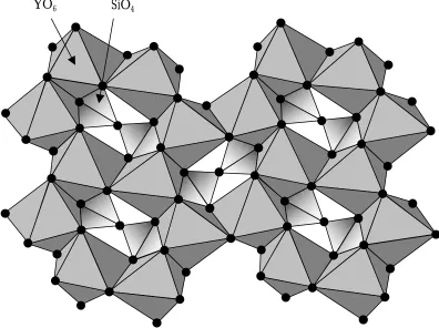
EOT < 1.0 nm with low tunneling. Figure 2.1a depicts the mineral keiviite (Y2Si2O7), which
consists of a Si2O76- structural unit with yttrium connecting the two corner sharing SiO4
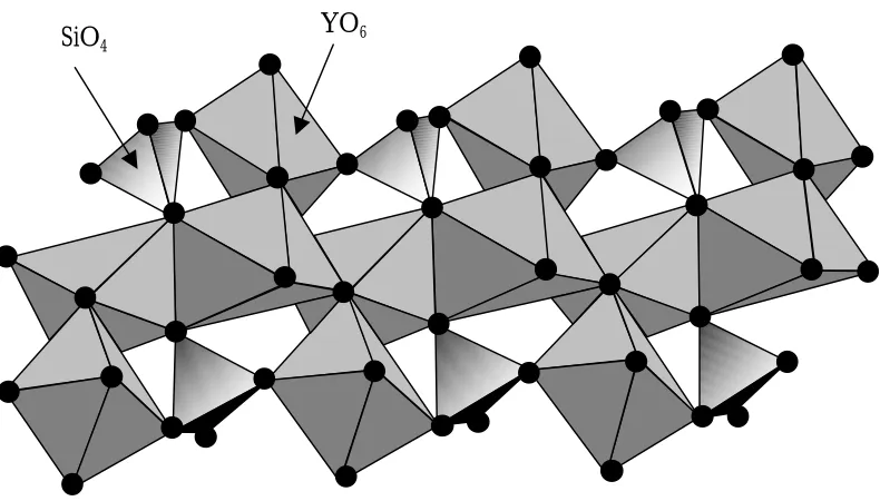
tetrahedra.3 Figure 2.1b shows the yttrium orthosilicate (Y2SiO5) structure where four of the oxygen atoms are bound in a silicon tetrahedron with each corner joining two yttrium octahedron and the fifth oxygen atoms, which are not involved with the silicon tetrahedron,
are shared between four yttrium octahedron in a rod-like chain.4 Y2O3⋅2SiO2 and Y2O3⋅SiO2
and a(Y2SiO5) = 1.041 nm are closely match with a (Si) = 0.543 and a(Si)⋅2 = 1.086 nm,
respectively. Also, yttrium silicate films exhibit low oxygen permeability and should provide
excellent passivation.5 These advantageous properties make yttrium silicate an suitable materials choice for CMOS technology.
We form yttrium silicate films on silicon by oxidation of yttrium silicide, where the silicide films are formed by vacuum annealing of yttrium films on cleaned silicon. A similar approach has been utilized elsewhere to investigate the oxidation properties of silicides,
where hafnium silicide is oxidized to from hafnium silicate.6 One problem with the oxidation of silicides is that oxidation does not always result in silicate formation, but results
in a SiO2 film on silicide, as in the case of nickel silicide and cobalt silicide.7 It has been
postulated that oxidation of a metal silicide will result in silicate formation if the metal-oxygen bond posses a more negative free energy of formation than the silicon-metal-oxygen
bond.8 Since the Y-O bond is stronger than the Si-O bond, we expect oxidation of yttrium silicide to result in silicate formation.
This article reports on the physical and electrical properties of yttrium silicate (Y-O-Si) as compared to the properties of SiO2 and Y2O3. X-ray photoelectron spectroscopy
(XPS) is used to compare the oxidation state of yttrium, silicon and oxygen in Y-O-Si, SiO2
and Y2O3. Fourier transform infrared spectroscopy (FTIR) is used to identify the Si-O and
Y-O vibrational modes in Y-O-Si, SiO2 and Y2O3. Y-O-Si film topology is investigated
2.2 EXPERIMENTAL
Substrates were p-type Si(100) with resistivity 0.1-0.3 Ω cm. Samples were prepared by dipping for 5 minutes in JTB 100 (a tetramethylammonium hydroxide based alkaline solution with a carboxylate buffer), rinsing in deionized water, etching in buffered hydrogen fluoride for 30 seconds with no final rinse and loading immediately into vacuum.
Y-O-Si films were formed by sputtering yttrium onto cleaned silicon, vacuum annealing and oxidizing in N2O. The exact composition of the films reported here is
unknown and we will denote our films as Y-O-Si or simply as yttrium silicate. Sputtering
was performed at 25 °C in 4.3 mTorr Ar, a radio frequency (rf) power of 420 W at 13.56 MHz and an yttrium target dc bias of –1000 V in a system with an ultimate vacuum of 5x10⁻⁸
Torr. The yttrium films on silicon were annealed in situ in vacuum (< 1x10⁻⁶ Torr) at 600 °C
to form yttrium silicide. The yttrium silicide was thermally oxidized ex-situ in a standard tube
furnace in 1 atm N2O at 900 °C. SiO2 films were thermally grown (∼100 nm) by wet
oxidation. Y2O3 films were formed by sputtering yttrium onto ∼50 nm SiO2 and oxidizing in
N2O for 20 minutes.
Y-O-Si films for XPS, FTIR and SEM analysis were formed by sputtering 240 nm of yttrium onto cleaned silicon, annealing in vacuum for 30 minutes and oxidizing in N2O for
20 minutes. XPS was performed ex situ using a Riber LAS3000 utilizing a single-pass, field
retarded cylindrical mirror analyzer and non-monochromatic Mg Kα (hν = 1253.6 eV).
Spectra were collected using 0.1 eV step sizes and a resolution of ∼1.0 eV. The binding
normalized to the silicon substrate. The thin SiO2 buffer that the Y2O3 films were formed
on was substracted from the Y2O3 FTIR spectra. High resitivity (15 Ω-cm) silicon wafers
were used for FTIR analysis to minimize free carrier absorption in the substrate. These substrates were single side polished and “orange peel” roughened on the backside to reduce background interference fringes.
Y-O-Si films for electrical testing were formed by sputtering 2.5 nm of yttrium onto
cleaned silicon, annealing in vacuum for 5 minutes and oxidizing at 900 °C in N2O for 15
seconds. Front-side electrical contact (no back-side metal employed) was made to the Y-O-Si films using a Four Dimensions CV map 92-A mercury probe. Capacitance measurements were taken at 1 MHz using a HP 4284a LCR meter.
2.3 RESULTS AND DISCUSSION
Chemical bonding in Y-O-Si, SiO2 and Y2O3 was investigated using XPS. Figure 2.2
presents the Y 3d photoelectron spectra for Y-O-Si and Y2O3. The Y 3d peak is a doublet
resulting from the Y 3d3/2 and the Y 3d5/2 (the more intense component where peak position
is referenced) components of the spin-orbit splitting. The Y 3d peak for Y2O3 is measured
at 156.8 eV binding energy (BE) and reported in the literature9 at 156.8 eV. The Y 3d peak for yttrium silicate is measured at 157.6 eV.
The Y 3d spectra for Y-O-Si and Y2O3 in Fig. 2.2 indicate that the yttrium in both
films is fully oxidized, since a metallic Y 3d peak at 156.0 eV is not observed.10 There is no evidence for Y-Si bonds (155.8 eV) in the yttrium silicate Y 3d spectrum. Since yttrium and silicon are only bonded to oxygen in the yttrium silicate crystal structures exhibited in Figs. 2.1a and 2.1b, the absence of Y-Si bonding in Y-O-Si films is expected. The Y 3d peak for Y-O-Si is shifted to higher BE than the Y 3d peak for Y2O3. This is likely due to increased
density donation from yttrium to oxygen in Y2O3, consistent with the relative
electronegativities of yttrium, silicon and oxygen (1.2, 1.8, 3.5 on the Pauling scale).
Figure 2.3 shows the Si 2p portion of the XPS signal for Y-O-Si and SiO2. The Si 2p
photoelectron peak position for SiO2 is measured and reported in the literature10 at 103.3
eV. The Si 2p photoelectron peak position for Y-O-Si is measured at 101.0 eV. The yttrium silicate Si 2p peak is shifted to lower BE than that for SiO2, indicating the silicon in yttrium
silicate is in a lower oxidation state than the silicon in SiO2. This is consistent with yttrium
donating electron density to the Si-O bond. The observation that the Y 3d and Si 2p peak positions for the Y-O-Si are different than either Y 3d in Y2O3 or Si 2p in SiO2 indicates the
presence of a uniform material with the absence of phase separated Y2O3 or SiO2.
Figure 2.4 presents the O 1s spectra for Y-O-Si, Y2O3 and SiO2. The peak positions
for the Y-O-Si, Y2O3 and SiO2 are 530.5, 529.25 and 533.0 eV, respectively. The shoulder
observed on the Y2O3 spectrum at 531.5 eV is assigned to O-H bonding in the film likely
acquired during post-deposition exposure to ambient water.9 The O 1s peak for Y-O-Si is measured to fall between Y2O3 and SiO2, as expected considering the electronegativity
differences between yttrium and silicon. Again, the absence of an O 1s peak for SiO2 or
Y2O3 in the Y-O-Si spectrum indicates the absence of any phase segregation in the silicate.
Analysis of the bonding environments in Y-O-Si, SiO2 and Y2O3 were investigated
using FTIR. Figure 2.5a presents the mid-IR region of the FTIR spectrum for Y-O-Si and Y2O3. The SiO2 FTIR spectrum presented in Fig. 2.5a exhibits three characteristic
vibrational modes of SiO2. The peaks located at 1077, 810 and 400 cm-1 are the Si-O-Si
asymmetric stretching, bending and rocking modes, respectively. These peaks are typical for a stoichiometric and relaxed amorphous SiO2 network. The dominant peak in the Y-O-Si
FTIR spectrum is broader and shifted to lower frequency, it is similar in shape to the asymmetric stretch measured at 1077 cm-1 and is assigned to Si-O stretching in the Y-O-Si.
The frequency shift and broadening of the Si-O stretch in the yttrium silicate is consistent with a weakening of the Si-O bond resulting from the combined effects of transfer of electron density from the yttrium to the Si-O bond and a wider distribution of Si-O bond angles available in the silicate. Figure 2.5b presents the far-IR region of the FTIR spectrum for Y-O-Si and Y2O3. The Y2O3 spectrum in Fig. 2.5b exhibits vibrational modes at 374, 335
and 303 cm-1 characteristic of Y-O stretching in Y
2O3.11 The Y-O-Si spectrum in Fig. 2.5b
displays two broad peaks assigned to Y-O stretching in the silicate.
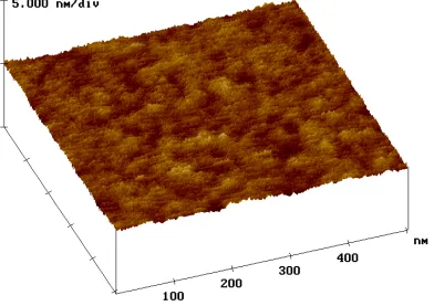
Figure 2.6 presents an AFM image of a Y-O-Si film with a root mean square surface roughness of 8.0 nm. It has been reported that vacuum annealing of yttrium films on silicon
forms an epitaxial silicide with grain sizes on the order of 70 nm.12 The roughness inherent in the yttrium silicide is consistent with the observed roughness in the Y-O-Si film.
Capacitance-voltage testing of Y-O-Si films was performed to ascertain their electrical quality and the results are depicted in Fig. 2.7. The equivalent oxide thickness
(EOT) for this film was calculated to be ∼5.0 nm. The ideal flat band voltage (Vfb) for a
mercury-oxide-semiconductor (Na = 1x1017 cm-3) is -0.55 V. Vfb for the C-V curve displayed
in Fig. 2.7 is calculated at –0.51 V, which corresponds to a fixed charge density of ∼9x10¹⁰
cm-2 and suggests the presence of negative fixed charges in the silicate.
2.4 CONCLUSIONS
We have shown the physical and electrical properties of Y-O-Si films formed on silicon by oxidation of yttrium silicide. The shift of the Y 3d photoelectron peak to higher BE compared Y2O3, the shift of the Si 2p peak to lower BE compared to SiO2 and the
Y-O-Si bonding structure. There is no evidence in the XPS spectra for the presence of SiO2,
Y2O3 or yttrium silicide. XPS spectra are consistent with FTIR spectra where a Si-O
stretching peak is measured at 950 cm-1 and Y-O stretching peaks are measured in the far-IR,
which are also consistent with the formation of Y-O-Si. These results are consistent with the donation of electron density from yttrium to the Si-O bond in the silicate. C-V measurements reveal that the Y-O-Si films are of low defect density. Based on these results,
we have investigated ultra-thin (EOT = ∼1.0 nm) Y-O-Si films and will report the results elsewhere.
2.5 ACKNOWLEDGEMENTS
2.6 REFERENCES
1 I. Barin, Thermochemical Data of Pure Substances (VCH Verlagsgesellschaft, Weinheim,
Germany, 1989).
2 M. Gurvitch, L. Manchanda, and J. M. Gibson, Appl. Phys. Lett. 51, 919-921 (1987).
3 N. G. Batalieva and Y. A. Pyatenko, Zhurnal Strukturnoi Khimii 8, 548-549 (1967).
4 B. A. Maksimov, V. V. Ilyukhin, Y. A. Kharitonov, and N. V. Belov, Kristallografiya
15, 926-933 (1970).
5 J. D. Webster, M. E. Westwood, F. H. Hayes, R. J. Day, R. Taylor, A. Duran, M.
Aparicio, K. Rebstock, and W. D. Vogel, J. European Ceram. Soc. 18, 2345-2350 (1998).
6 S. P. Murarka and C. C. Chang, Appl. Phys. Lett. 37, 639-641 (1980).
7 F. M. Dheurle, Thin Solid Films 105, 285-292 (1983).
8 S. P. Murarka, J. Vac. Sci. Technol. 17, 775 (1980).
9 O. G. Alekseev, N. V. Krivosheev, M. Y. Khodos, V. R. Galakhov, V. V. Shumilov,
V. M. Cherkashenko, E. Z. Kurmaev, and V. A. Gubanov, Inorg. Mater. 22, 1748-1751 (1986).
10 J. F. Moulder, W. F. Stickle, P. E. Sobol, and K. D. Bomben, Handbook of X-ray
Photoelectron Spectroscopy (Perkin-Elmer Corporation, Eden Prairie, MN, 1992).
11 Y. Nigara, M. Ishigame, and T. Sakurai, J. Phys. Soc. Japan 30, 453 (1971).
Figure 2.1a Schematic depicting crystal structure of Y2Si2O7.
Figure 2.1b Schematic depicting crystal structure of Y2SiO5.
YO6
Figure 2.2 Y 3d portion of the XPS spectra for Y-O-Si and Y2O3.
Intensity (a.u.)
162
160
158
156
154
152
150
148
Binding Energy (eV)
Y
2O
3Y-O-Si
Figure 2.3 Si 2p portion of the XPS spectra for Y-O-Si and SiO2.
Inte
nsity (a.u.)
110
105
100
95
90
Binding Energy (eV)
SiO
2
Y-O-Si
Figure 2.4 O 1s portion of the XPS spectrum for Y-O-Si, Y2O3 and
SiO2.
Inte
nsity (a.u.)
535
530
525
520
Binding Energy (eV)
SiO
2
Y-O-Si
Y
2
O
3
O 1s
Inte
nsity (a.u.)
4000
3000
2000
1000
Wavenumber (cm
-1)
SiO
2
Y-O-Si
Inte
nsity (a.u.)
600
500
400
300
200
100
Wavenumber (cm
-1)
Y-O-Si
Y
2
O
3
700
600
500
400
300
200
100
0
C (pF/c
m
2
) x10
3
-4
-3
-2
-1
0
1
2
V
g(V)
Chapter 3 is a reprint of a manuscript to be submitted to the Journal of Applied Physics
PHYSICAL AND ELECTRICAL CHARACTERIZATION OF YTTRIUM
SILICATE HIGH-K DIELECTRICS
J. J. Chambers and G. N. Parsons
ABSTRACT
The physical and electrical properties of yttrium silicate thin films are described. The reactivity of yttrium metal with silicon and oxygen is exploited to form interface layer free yttrium silicate thin films. X-ray photoelectron spectroscopy (XPS) and Fourier transform infrared spectroscopy (FTIR) are used to determine chemical bonding and composition of yttrium silicate films. Capacitance-voltage testing is used to determine the quality of the dielectric and the electrical thickness. The oxidation of yttrium on silicon to form
amorphous yttrium silicate films (∼40 Å) with EOT ≅ 1.0 nm has been demonstrated. We establish that the oxidation of yttrium silicide also results in an yttrium silicate film. The oxidation of yttrium on silicon results in a films nearly identical, although with a lower silicon fraction, to films formed by the oxidation of yttrium silicide. These results suggest that the yttrium silicate forms through a competition between yttrium-silicon reaction and oxidation. This competition results in an yttrium silicate film for thin (<40 Å) initial yttrium coverage and in an Y2O3/Y-O-Si bi-layer at thick (>80 Å) initial yttrium coverage. Analysis
slow oxidation during consumption of the silicon substrate. It is the high reactivity of yttrium that enables complete oxidation of the yttrium silicate while avoiding excessive oxidation of the silicon substrate. In principle, the oxidation of other metals on silicon of the metal oxides of interest as high-k dielectrics (such as, ZrO2, HfO2 and La2O3) is expected
CHAPTER 3
PHYSICAL AND ELECTRICAL CHARACTERIZATION OF YTTRIUM
SILICATE HIGH-K DIELECTRICS
3.1 INTRODUCTION
The semiconductor industry improves performance by decreasing the gate length with each successive complementary metal oxide semiconductor (CMOS) device generation. With each generation, the silicon dioxide gate dielectric thickness scales with gate length to promote high channel transconductance. The International Technology Roadmap for
Semiconductors predicts that a 50 nm device generation will require the equivalent of a sub-1.0
nm silicon dioxide.1 Reducing the silicon dioxide thickness to the sub-1.0 nm regime may
not be feasible because significant leakage and reliability issues become major concerns
below ∼2.0-1.5 nm2 due to direct tunneling, which is exponentially dependent on the
dielectric thickness. Maintaining low tunneling current requires an increase in the gate dielectric thickness and an accompanying increase in the dielectric constant (k), since capacitance scales as k/thickness, to obtain the desired equivalent silicon dioxide thickness (EOT).
A variety of metal oxides, including Y2O3, Ta2O5, TiO2, HfO2, ZrO2 and Al2O3, have
been suggested as high-k (k > kSiO2 = 3.9) replacements for silicon dioxide.
3-8 A Ta
2O5 (k ≅
25) gate dielectric can be made approximately 6 times thicker than the equivalent silicon dioxide gate, assuming the silicon/high-k interface does not contain any SiO2, which would
material. Thermodynamic calculations have been used to evaluate the stability, with respect to no silicide or SiO2 formation, of binary metal oxides in contact with silicon. Y2O3, ZrO2,
HfO2 and the rare earth oxides are the most promising binary metal oxides from using this
thermodynamic analysis.9 However, pure metal oxides tend to crystallize at relatively low
temperatures10 resulting in possible high conductivity pathways along grain boundaries
counteracting the benefits of the high-k dielectric. Therefore, scaling the gate insulator into the sub-1.0 nm regime requires a material with suitably high-k that remains stable and amorphous during typical annealing cycles.
Recently, zirconium silicate and hafnium silicate have been demonstrated as potential
high-k gate dielectrics with k ∼ 11 and an amorphous microstructure after annealing at 1050
°C for 20 seconds.11 Yttrium silicate also possesses desirable thermodynamic, dielectric and
structural properties that make it attractive as a high-k candidate. The Y-O bond is quite
strong, since the free energy of formation per oxygen atom (-∆Gf) (at 25 °C) is 2.40x10⁻²²
kcal for Y2O3 compared to 1.70x10⁻²² kcal for SiO2.12 The mineral keiviite (Y2Si2O7) (Fig.
3.1a) consists of a Si2O76- structural unit with yttrium connecting the two corner sharing SiO4
tetrahedra.13 In the yttrium orthosilicate (Y
2SiO5) structure (Fig. 3.1b), four of the oxygen
atoms are bound in a silicon tetrahedron where each corner joins two yttrium octahedron, and the fifth oxygen atoms, which are not involved with the silicon tetrahedron, are shared between four yttrium octahedron arranged in a chain.14 Y
2Si2O7 and Y2SiO5 exhibit low
lattice mismatch with silicon, since the lattice constants a(Y2Si2O7) = 0.554 nm and a(Y2SiO5)
= 1.041 nm are closely match with a(Si) = 0.543 and a(Si)⋅2 = 1.086 nm, respectively.13,14
phase diagrams of the group IV silicates (i.e. zircon and hafnon)15 where the two-phase
regions are silicate with metal oxide or SiO2. Yttrium silicate films exhibit low oxygen
permeability and should provide excellent passivation.16
Previous studies have demonstrated the formation of yttrium silicate by the
oxidation of yttrium on silicon in dry air at 500-700 °C.3 Yttrium silicate films with the
composition Y2.45Si0.55O5 approximately 26.0 nm thick were created using this process.
Capacitance measurements on MOS capacitors with an Al/Y2.45Si0.55O5/Si structure yielded
k∼12 for the silicate layer, which should be suitably large to obtain EOT < 1.0 nm with low tunneling. These films also exhibited acceptable current-voltage and breakdown characteristics.
Formation of YSi2-x by vacuum annealing of yttrium films on silicon is a
well-characterized process where the silicide is formed by the fast diffusion of silicon into the
metal film.17,18 Hexagonal YSi
2-x films have been epitaxially grown on Si(100) by annealing
yttrium films on silicon above 550 °C in vacuum.19 Yttrium silicide formation occurs at
relatively low temperatures (120 to 140 °C) and at a very rapid rate (estimated as 40 to 50
Å/s at 350 °C).20 Furthermore, films created in this manner have been found to oxidize up
to ∼15 times faster than crystalline silicon.21 This creates a situation where thin yttrium
silicate films can be formed on silicon with minimal or no oxidation of the underlying silicon substrate.
The possibility of forming silicate materials on silicon by oxidizing the metal silicide is intriguing. The oxidation of silicides has been addressed in terms of the free energy of
formation per oxygen atom (-∆Gf) for metal oxides compared with that of SiO2.22 If the
Conversely, if the -∆Gf of a metal oxide is greater than that of SiO2, the metal oxide can
reduce SiO2. It has been proposed that oxidizing a metal silicide where the metal oxide has a
-∆Gf greater than that of SiO2 will result in a mixed metal oxide/SiO2 film and oxidizing a
metal silicide where the metal oxide has a -∆Gf less than that of SiO2 will result in
preferential oxidation of silicon.22 Table 3.1 presents -∆G
f for a variety of metal oxides and
the expected oxidation product of the metal silicide on silicon. For example, the oxidation of MoSi2, WSi2 and TaSi2 (see Table 3.1) on silicon has been reported to result in the
formation of a metal-free SiO2 film on a silicide layer over silicon.23-25 The SiO2 forms
through the oxidation of silicon that has diffused through the silicide, which remains stable. The silicides were found to oxidize only when the silicides were on SiO2 or polycrystalline Si
on SiO2, where there is a limited supply of silicon. However, the oxidation of hafnium
silicide has been demonstrated to result in an Hf-O-Si layer.26 Y
2O3 has a greater -∆Gf than
SiO2. Therefore, yttrium silicide is expected to oxidize to form a Y-O-Si film. It is worth
noting that, for other metal oxides of interest as high-k dielectrics, oxidation of their respective metal silicide is expected to result in a metal-O-Si film.
an oxidizing ambient results in oxidation of the silicide, and the oxidation of yttrium on silicon results in the mixing of yttrium and silicon. The extreme reactivity of yttrium with
silicon and oxygen enables the formation of interface-free Y-O-Si thin (∼40 Å) films using
the methods described in this article. Y-O-Si films with EOT ≅ 1.0 nm are demonstrated, which encourages further study of films formed by oxidation of yttrium on silicon and oxidation of yttrium silicide.
3.2 EXPERIMENTAL
3.2.1 SPUTTERING AND SURFACE PRETREATMENT SYSTEM
Yttrium films were sputtered in the two-chamber vacuum system shown in Fig. 3.2. The system is equipped with a load-lock and a plasma processing chamber. A base pressure of 1x10⁻⁷ Torr is attained in the load-lock using a hybrid-turbo and dry diaphragm pumping
system. Silicon samples are transferred from the load-lock to a manipulator with full X, Y, Z
and θ motion in the processing chamber. A base pressure of 5x10⁻⁸ Torr in the processing
shield. The Ar, N2 and N2O process gas flows are supplied to the chamber through the
front of the plasma tube and regulated from 1-100 sccm (N2) with mass flow controllers.
The processing chamber is equipped with a retractable yttrium (99.1%, Ta as the major impurity) sputter target that can be isolated from the system by a gate valve. A 200 W DC power supply provides up to -1000 V of bias to the sputter target and is run in a constant
voltage mode. A 600 W radiant heater enables substrate temperatures up to 650 °C. All post-deposition vacuum anneals were performed in situ. The plasma processing chamber is also compatible with in situ plasma oxidation, which will be presented in a separate publication. For the results in this article, oxidation is performed ex situ from the processing
chamber in a standard 10 cm diameter tube furnace at temperatures from 500-900 °C in 1 atm N2O or air.
3.2.2 SAMPLE PREPARATION
Substrates were n- (1.0-2.0 Ω-cm) or p-type (0.1-0.3 Ω-cm) Si(100) cut from
commercial wafers into 2.5 X 2.5 cm samples. Samples were prepared by dipping for 5 minutes in JTB 100 (a tetramethylammonium hydroxide based alkaline solution with a carboxylate buffer), rinsing in deionized water (DI), etching in buffered hydrogen fluoride (HF) for 30 seconds with no final rinse and loading immediately into vacuum.
3.2.3 SPUTTER CONDITIONS
Sputtering was performed at room temperature in 4.3 mTorr Ar and an rf power of 420 W. During sputtering, the yttrium target was fully extended into the plasma and biased at –1000 VDC. Yttrium metal is reactive, and residual oxygen or water in the system will affect the target surface and sputter rate. To control this problem, the target was conditioned before loading samples and performing runs by sputtering for 30-60 minutes at