The Design of a Hardware Memory
Allocator Based on the Buddy System
Manyip Ngan
Edward F. Gehringer
July 1995
Technical report 95-10,
CONTENTS PART A
1. Introduction 1
2. System Design 1
2.1 Bit-Vector 2
2.2 Memory Allocation 3
3. System Description 4
4. Conclusion 8
PART B
1. System Description 9
1.1 General Functional Description 9
1.2 Pin Description 9
1.3 Simulation Block Diagram 9
2. Functional Block Description 10
2.1 I/O Latches 10
2.2 Rounded_up 10
2.3 CBT 11
2.3.1 Allocation/free Scheme 12
2.3.1.1 Allocation Scheme 12 2.3.1.2 Deallocation Scheme 17
2.3.2 CBT Block Diagram 19
2.3.3 Pin Description 20
2.4 Selector 20
2.5 MEM 22
2.6 2-1 MUX 24
2.7 4-16 Decoder 24
2.8 16-4 Encoder 24
2.9 Error Detection 24
3. System Data Flow 25
3.1 Allocation Operation 25
3.1.1 Functional Timing 25
3.1.2 Data Flow 26
3.2 Deallocation Operation 28
3.2.1 Functional Timing 28
3.2.2 Data Flow 29
4. Circuit Description 31
4.1 CBT 31
4.1.1 Generation of Availability 32 4.1.2 Find the first ABRS (allocation block of 32
requested size)
ii
4.2 Other Blocks 43
4.2.1 MEM 43
4.2.2 Selector 44
4.2.3 Rounded_up 47
4.2.4 2-1 MUX 48
4.2.5 16-4 Encoder 48
4.2.6 4-16 Decoder 48
4.2.7 Latches 48
5. Simulation Result 49
5.1 Functional Timing 49
5.1.1 Allocation/allocation Cycles 49 5.1.2 Deallocation/deallocation Cycles 50 5.1.3 Allocation/deallocaton/allocaion Cycles 50 5.1.4 Allocation/nop/allocation Cycles 51 5.1.5 Deallocation/nop/deallocation Cycles 51 5.2 Gate Delay and Simulation Pins 51
5.2.1 Gate Delay 52
5.2.2 Simulation Pins 52
5.3 Test Patterns and Simulation Waveforms 53
5.3.1 Allocation Test 54
5.3.2 Deallocation Test 55
5.3.3 Mixed Test 56
5.4 Discussion of AC timing 56
5.5 Discussion 58
Circuits 59
Simulation Waveforms 77
PART A
1. Introduction
Dynamic memory management has been an important topic in
computer systems for many years. Much research on has been carried out on high-performance algorithms. Most of this research focuses on improving memory-management performance through software implementation.
The paper “A high-performance memory allocator based on the buddy system,” written by J. Morris Chang and Edward F. Gehringer, proposes a novel hardware implementation of the buddy system. This implementation uses bit-map tables to represent the allocation status of cache lines, and is capable of allocating one of these lines in a single cycle.
Using Viewlogic simulation tools, we designed the circuits for this hardware implementation. Our work includes architecture design, circuit design, debugging, and testing. In this report, we present the design concept of this system. The remainder of this report is organized as follows. Section 2 presents the basic idea of system design and section 3 presents the functional timing of allocation and deallocation examples. A brief conclusion will come after section 3. A detailed discussion of the system, its circuits, and
simulation results will be covered in Part B.
2. System Design
Object-oriented systems create objects very frequently. Each object occupies a certain amount of memory. In an object-oriented system, memory allocation thus occurs very frequently. Most objects, however, do not “live” very long. That is, after a short period of time, most objects are no longer pointed to by a pointer anywhere in memory. They have effectively been abandoned, and the memory manager may reclaim them.
The memory allocator described in this document implements memory allocation and deallocation. This section addresses its design.
2.1. The bit-vector
Our memory allocator uses a bit-vector to represent the allocation status of each cache-line-size block of virtual memory. A bit has the value 1 if the corresponding block is allocated, and 0 if the corresponding block is free. In order to avoid unnecessary memory reads, all blocks will be allocated in cache. That is, when an allocation occurs, the memory at the allocation address is not read into the cache; rather the target cache line is cleared. When an object dies in cache, the dead object is not written back to memory; its cache line(s) are simply marked as free. A simple example of using a bit-vector to manage 211 = 2048 blocks is shown in the figure below.
111110000...0000
111111110...0000
request creation of object
that has size of 3 blocks 0000 0000 101 00000 bit vector ( 2048 bits)
address :
block # offset
assume each block is 32 bytes *
*
A program’s memory may consist of a very large number of cache-sized blocks. A very large bit-vector would be needed to represent the allocation status of each block. Since it is not very efficient to manipulate large bit-vectors in hardware, the virtual address space is divided into regions, each of which has its separate (smaller) bit-vector.
The bit-vector for a region is held in a series of registers. Each register contains a portion of the bit-vector that represents the allocation status of a particular page of memory. The reason for dividing the bit-vector into page-sized chunks is that most caches are accessed by physical address, while programs reference virtual addresses. A bit-vector represents the allocation status of a region of virtual memory, which is (usually) not contiguous in physical memory. So each page-sized bit-vector may refer to an area of physical memory which is discontiguous from the physical memory of its virtual neighbors. The diagram below shows how this works. In the
. . . .
. .
page frame # bit-vectors (128 bits each)
16 entries
Two major functions of the memory allocator are memory allocation and deallocation. The following sections will describe how our bit-vectors can be used for that purpose.
2.2. Memory allocation
Allocating free memory space to a new object requires searching for an appropriate number of free bits in a bit-vector. In our system, we divide the bit-vector of a virtual-memory region into 16 bit-vectors, each representing one page of memory. The first step is a best-fit search to locate a page that has a free block large enough to allocate the requested block. Associated with each page in the region, there is an availability vector indicating the size of the largest free block in that page. The page is selected and its bit-vector is read out for use in the second step.
When the bit-vector is read out, it is passed through a set of logic gates that construct a complete binary tree (CBT). When a block of the requested size is located using the CBT, the allocation address is output and the bits
. . .
. . .
base page # page frame # bit-vectors (128 bits each) availability vectors
128 bits CBT
page frame # page offset
page # page offset index
1
2
3a
3b
a
b c
1 2 3a
3b a
b
c
free memory space request
bit-vector read out
bit-vector update
availability-vector update
physical address
virtual address
index can be obtained in 2
. . .
3. System Description
The memory allocator allocates or deallocates memory in one single clock cycle. In allocation operation, one can create an object by specifying the requested memory size (object size) and setting the operation mode to allocation. The external pins for user to input these two signals are:
B[7:0] — memory size (for both allocation and deallocation operation) ALLOC — operation mode switch (ALLOC = '1' is allocation mode and
ALLOC = '0' is deallocation mode) When the system receives an allocation request and has enough free space to allocate the memory, it will send out the starting address of the allocated memory block without signaling an error (ERROR = '1'). If the allocation is not successful, the system will return an invalid address while signaling an error (ERROR = '0'). The external pins for outputing these two signals are: ADDR_OUT[10:0] — starting address of the allocated memory
For example, if user creates an object of size = 7 lines, he needs to: . set B[7:0] = 7 = 07 in hexadecimal
. set ALLOC = 1
If the allocation process is successful, the system will return the starting address of the allocated memory and set ERROR pin to '1'. In this example, we assume the starting address is 018 in hexadecimal. CLK1 and CLK2 are two non-overlapping clock signals used to synchronize the internal circuits. The functional timing of this allocation cycle is shown below:
CLK1
CLK2
ALLOC
B[7:0]
ADDR_OUT[10:0]
ERROR
cycle allocation
'1 ' means allocation
07
018
'1 ' means no error
In this allocation cycle, the requested memory size (B[7:0] = 07) and operation mode (ALLOC = 1) are input at the rising edge of CLK1. The system outputs the starting address of newly allocated memory (ADDR_OUT[10:0] = 018) without error (ERROR = 1) at the rising edge of CLK2 in the same cycle.
In deallocation operation, one can free an object by specifying the deallocation memory size (size of object), the address of the memory, and the operation mode at the beginning of the cycle. The external pins for these three signals are B[7:0], ADDR_IN[10:0], and ALLOC. At the end of the cycle, the system will set ERROR to '1' when operation is successful and set ERROR to '0' when the deallocation fails.
For example, if user frees an object located at address 010 and had a size of 5 blocks, he needs to:
. set B[7:0] = 5 = 05 in hexadecimal . set ADDR_IN[10:0] = 010
The functional timing for this example is shown below:
CLK1
CLK2
ALLOC
B[7:0]
ERROR
cycle deallocation
05
'1 ' means no error '0' means deallocation
The system will return ERROR = '1' at the rising edge of CLK2 in the same cycle when the deallocation is successful.
All external pins are listed below:
Pin name In/output Function Used in which mode?
B[7:0] input memory size alloc. and dealloc.
ALLOC input operation mode switch: ALLOC = '1' for allocation, ALLOC = '0' for deallocation
alloc. and dealloc.
ADDR_IN[10:0] input starting address of memory
requested to be freed deallocation only ADDR_OUT[10:0] output starting address of memory
requested to be allocated
allocation only
ERROR output error signal:
ERROR = '1' when no error exists, ERROR = '0' when error exists
alloc. and dealloc.
During development, three test patterns are used for the AC timing test. The system works well within a 75ns clock rate. The testing includes:
• Allocation / Allocation cycles • Deallocation / Deallocation cycles
• Allocation / Deallocation / Allocation cycles • Allocation / Nop / Allocation cycles
• Deallocation / Nop / Deallocation cycles
The simulation is done in the Viewlogic environment with the gate delay set to the following value:
Table 2.2
G Gate Type TPLH, TPHL TPLZ, TPHZ,
TPZL, TPZH
CLKtoQ0, CLKtoQ1,
CLKtoQN0, CLKtoQN1
NOT 0.5 ns — —
BUF 1.0 ns — —
TRIBUF 1.2 ns 1.2 ns —
NAND 2 inputs
3 inputs
4 inputs
0.8 ns
0.8 ns
1.0 ns
—
—
—
—
—
—
NOR 2 inputs
3 inputs
4 inputs
0.8 ns
0.8 ns
1.0 ns
—
—
—
—
—
—
AND 2 inputs
3 inputs
4 inputs
0.8 ns
0.8 ns
1.0 ns
—
—
—
—
—
—
OR 2 inputs
3 inputs
4 inputs
0.8 ns
0.8 ns
1.0 ns
—
—
—
—
—
—
LATCH — — 7.5 ns
T_F/F — — 3.5 ns
D_F/F — — 7.5 ns
Legend:
TPLH — low to high propagation time TPHL — high to low propagation time
4. Conclusion
The system works well with a clock cycle of 75 ns. It cannot work faster than this speed because the whole architecture is designed to generate the output within one clock cycle. There are two possible ways to improve our system speed.
1. Use a pipelined architecture to separate the system into several smaller segments. This allows several allocation or deallocation requests to be handled at the same time and increases the throughput.
2. Reduce the delay time by optimizing the circuits.
As we are entering the world of object-oriented programming, further hardware design should be done to enhance the speed of creating or
PART B
1. System Description
1.1 General Function Description
The memory allocator is a hardware implemetation based on the paper “A high-performance memory allocator based on the buddy system.”
Information about the allocation status of memory blocks is held in a binary tree structure formed by AND/OR/FLIPPER cells. These cells propagate information about allocation status and realize the allocation and
deallocation operations. The system can allocate or deallocate an arbitrary-sized block in a single clock cycle. The bit-map for allocating memory is maintained by a set of 16 bit-vectors, each of which contains 128 mapping bits. 1.2 Pin Description
The pin functions are listed in table 1.1.
Table 1.1
CLK1 Clock 1 — Cooperates with CLK2 to provide two nonoverlapped clock signals to the internal circuits.
CLK2 Clock 2 — Cooperates with CLK1 to provide two nonoverlapped clock signals to the internal circuits.
CLR Clear pin — Clears the previous circuit’s status. Reset the circuits to the initial state.
ALLOC Operation mode switch — Set system to allocation mode when ALLOC = '1'. Set system to deallocation mode when ALLOC = '0'.
B[7:0] Memory size — Specify the number of memory blocks needed to be allocated or deallocated.
ADDR_IN[10:0] Input address — Specify the starting address of the deallocated memory blocks.
ADDR_OUT[10:0] Output address — Output the starting address of the allocated memory blocks.
ERROR Error pin — When the requested value (B[7:0]) is lager than 128 or the system has not enough memory to be allocated, the ERROR pin will be set "L". In normal operation, it is always set to "H".
1.3 Block Diagram of circuits
2. Functional Block Description
The whole system is composed of the following functional blocks. 2.1 I/O Latches
I/O latches synchronize the input and output signal/data with the CLK1 and CLK2 signals. There are five I/O latches in all, which are classified as input and output latches:
The input latches are all triggered by the rising edge of CLK1. They include:
N a m e Function
LATCH_A Latches in the memory size from the external signal B[7:0].
LATCH_B Latches in the starting address of the memory to be freed from the external signal ADDR_IN[10:0].
LATCH_C Latches in the operation mode signal from external pin ALLOC.
The output latches are all triggered by the rising edge of CLK2. They include:
N a m e Function
LATCH_D latches out the starting address of allocation memory to external pins ADDR_IN[10:0].
LATCH_E latches out the error signal to external pin ERROR.
2.2 ROUND_UP
ROUND_UP
OUT0
OUT1 OUT2 OUT3 OUT4
OUT5
OUT6 OUT7
ERROR
FLIP_ALL IN0
IN1
IN2 IN3
IN4
IN5 IN6
IN7
The size of the requested block B is rounded_up to generate the internal signal Brounded_up. Brounded_up is defined as:
Brounded_up = 2 log B
If the size of the requested block is so large that all 128 of the bits need to be flipped, the FLIP_ALL signal will be asserted. Here are some examples of Brounded_up, FLIP_ALL, and ERROR generated from a requested block size of 8 bits:
B [7:0] log B
log B
2 FLIP_ALL ERROR (low-active)
00000100 2 00000100 ( 22 ) 0 1
00010000 4 00010000 ( 24 ) 0 1
01000000 6 01000000 ( 26 ) 0 1
00000011 2 00000100 ( 22 ) 0 1
00001010 4 00010000 ( 24 ) 0 1
00010010 5 00100000 ( 25 ) 0 1
00101101 6 01000000 ( 26 ) 0 1
10000000 7 10000000 ( 27 ) 1 1
01000001 7 10000000 ( 27 ) 0 1
10000010 exceeds limit not valid 0 0
The maximum number of blocks requested at a time is 128, which is the total number of mapping bits in each bit-vector. If the requested block size is larger than 128, the system cannot handle this request, and ERROR will be set to '0'. The Brounded_up is not valid when ERROR is '0'. Otherwise, if the
requested block size is exactly equal to 128, the FLIP_ALL pin will become '1' to inform the CBT to allocate all 128 mapping bits in the selected bit-vector. The Brounded_up is used by SELECTOR block to select the appropriate bit-vector and also by the CBT to allocate/deallocate the requested mapping bits.
2.3 CBT
2.3.1 Allocation/free scheme
The CBT can allocate arbitrary requested block size when it has located sufficient free mapping bits in the bit-vector under the following schemes: 2.3.1.1 . Allocation scheme:
User attempts to allocate a memory block of size B. System will try to flip the
corresponding number of bits in a suitable bit-vector.
Find enough contiguous free mapping bits, corresponding to an allocation block of requested size (ABRS).
If more than one ABRS exists, choose the one with the lowest address. This is the best ABRS.
Allocate the B mapping bits in the location of the best ABRS.
Output the starting address of the best ABRS. This is also the starting address of the allocated blocks.
ADDR_OUT[6:0] ...
b0 b1 b127
current bit-vector
...
size of ABRS = 2 log B = 2 n
2. In the ABRS, the 2n mapping bits must be contiguous and share the common level-n node on the complete binary tree (CBT) structure. For example, for a 8-mapping-bit CBT.
level 3
level 2
level 1
level 0
The mapping bits are the nodes on level 0. A level-1 node has two level-0 children. We say the two children share the same level-1 node. Similarly a level-2 node has four level-0 children. Therefore, these four children are sharing the same level-2 node.
Here are the ways for locating ABRS in the mapping bits of size 2n. For n = 0, the mapping bits found
must share the same level-0 node. Each node and its children form an ABRS. As there are eight level-0 nodes, there are eight possible ABRSs.
level 3
level 2
level 1
level 0
For n = 1, there are four level-1 nodes, so there are four possible
ABRSs. level 3
level 2
level 1
For n = 2, there are two level-2 nodes, so there are two possible
ABRSs. level 3
level 2
level 1
level 0
For n = 3, there is one level-3 node,
so there is only one possible ABRS. level 3
level 2
level 1
level 0
If more than one possible ABRS exists, the CBT will choose the one with the lowest starting address, which is the first one on the left in the diagram. To illustrate the allocation scheme, we use an allocation example on a 8-bit bit-vector. Assume the user allocates memory five times and the requested block size are 1, 2, 3, 1 respectively. Assume all bits (mapping bits) on the bit-vector are ‘0’ ( free ) initially.
Allocate a memory block of size 1.
level 3
level 2
level 1
level 0 requested size
= 1
Before allocation 0 0 0 0 0 0 0 0
After allocation 1 0 0 0 0 0 0 0
allocated
Allocate memory of size 2.
level 3
level 2
level 1
level 0 requested size
= 2
Before allocation 1 0 0 0 0 0 0 0
After allocation 1 0 1 1 0 0 0 0
allocated
As the requested size = 2 = 21, the size of ABRS is also 21. There are 3 possible ABRSs. The CBT will choose the first one on the left.
Allocate memory of size 3.
level 3
level 2
level 1
level 0 requested size
= 3
Before allocation 1 0 1 1 0 0 0 0
After allocation 1 0 1 1 1 1 1 0
allocated
Allocate memory of size 1.
level 3
level 2
level 1
level 0 requested size
= 1
Before allocation 1 0 1 1 1 1 1 0
After allocation 1 1 1 1 1 1 1 0
allocated
As the requested size = 1 = 20, the size of ABRS is also 20. There are 2 possible ABRSs, and the CBT will cloose the first one on the left.
After the allocations, the mapping bits in the bit-vector change from 00000000 to 11111110.
There will be an error if there is no possible ABRS found for an allocation request. Therefore, ROUND_UP and SELECTOR blocks will check if a possible ABRS exists or not. If at least one exists, the CBT will be enabled (ENABLE pin is set to ‘1’). If no possible ABRS is found, CBT is disabled (ENABLE pin is set to ‘0’) and no mapping bit will be affected.
2.3.2. Deallocation scheme
...
b0 b1 b127
current bit-vector
... Size of the requested deallocation blocks
Starting address of the requested deallocation blocks
Deallocate the corresponding mapping bits on the current bit-vector
For deallocation operation, the user must supply the size and the starting address of the memory blocks he wants to free. The CBT will free the blocks that are allocated through the allocation scheme discussed in the previous part. This means that the address supplied must be the starting address of a possible ABRS for that size. Otherwise, an error may occur.
For example, for an 8-bit bit-vector:
Free 1 memory block at address a3 (assume the initial bit-vector is 11111111).
level 3
level 2
level 1
level 0 requested size
= 1
Before Free 1 1 1 1 1 1 1 1
After Free 1 1 1 0 1 1 1 1
Free Address a0 a1 a2 a3 a4 a5 a6 a7
the starting address. In this example, the user addresses a3. The resulting level-0 bit-vector is 11101111.
Free 2 memory blocks at address a4 (assume the initial bit-vector is 11111111).
level 3
level 2
level 1
level 0 requested size
= 2
Before Free 1 1 1 1 1 1 1 1 After Free 1 1 1 1 0 0 1 1
Free Address a0 a1 a2 a3 a4 a5 a6 a7
For size = 2, there are four possible ABRSs. The starting address for these ABRSs are a0, a2, a4, and a6. User can assign any one of them as the starting address. In this example, the user addresses a4. The resulting bit-vector is 11110011.
Free 3 memory blocks at address a4 (assume the initial bit-vector is 11111111).
level 3
level 2
level 1
level 0 requested size
= 3
Before Free 1 1 1 1 1 1 1 1
After Free 1 1 1 1 0 0 0 1
Free Address a0 a1 a2 a3 a4 a5 a6 a7
Free 5 memory blocks at address a0 ( assume the initial bit-vector is 11111111).
level 3
level 2
level 1
level 0 requested size
= 5
Before Free 1 1 1 1 1 1 1 1
After Free 0 0 0 0 0 1 1 1
Free Address a0 a1 a2 a3 a4 a5 a6 a7
For size = 5, there only one possible ABRS. The starting address must be a0. In this example, the user addresses a0 correctly. The resulting bit-vector is 00000111.
2.3.2 The CBT block diagram
PRE_RDUP[6:0]
POST_RDUP[6:0]
ADDR_IN[6:0]
FLIP_ALL
ENABLE
ADDR_SEL
IN[127:0] FLIP[127:0] ADDR_OUT[6:0] from LATCH_A
from ROUND_UP
to LATCH_D
from ROUND_UP
from LATCH_C
to MEM from LATCH_B
7
7
128
128 7
2.3.3 Pin description
N a m e Input/Output Function
PRE_RDUP[6:0] input Pre_roundup requested block size
POST_RDUP[6:0] input Post_roundup requested block size
The PRE_RDUP and POST_RDUP are used to find out the location of bits expected to be allocated or deallocated.
ADDR_IN[6:0] input Input address. This is the starting address of the deallocating memory blocks specified by user.
ADDR_OUT[6:0] output Output address. This is the starting address of the allocated memory block.
FLIP_ALL input Flip_all pin. When this pin is '1', the CBT will allocate all 128 mapping-bits in the bit vector.
ENABLE input Enable pin. The CBT will be disabled when ENABLE = '0' and will be activated when ENABLE = '1'.
ADDR_SEL input Address-select pin. When ADDR_SEL = '1', the CBT runs in allocation mode and allocates the memory blocks specified by the starting address generated internally. When ADDR_SEL = '0', the CBT runs in deallocation mode and frees the memory blocks specified externally from ADDR_IN[6:0].
IN[127:0] input IN bus. This inputs the 128 mapping bits of the bit-vector from the MEM block.
FLIP[127:0] output FLIP bus. This contains 128 bits. The CBT sets the flip bit to '1' when it allocates or deallocates the corresponding mapping bit. Otherwise, the flip bit is always set to '0'.
2.4 SELECTOR
There are 16 bit-vectors in the MEM block. Each bit-vector contains 128
Scheme of operation:
request to allocate block of size B
ROUND_UP
SELECTOR Compare the Brounded_up with the the values in 16 availability vectors. Then choose the appropriate vector by sending the selected vector address to the MEM block.
B
Brounded_up
availability vector 0 availability vector 1
availability vector 14
availability vector 15 .
. . . . .
MEM
. . . . .
. Error
selected vector address
The SELECTOR chooses one of the 16 bit-vectors by the following algorithm: if (there are availability vectors that have a run of exactly as many zero bits as specified by Brounded_up)
{
if the number of such availability vectors is more than one Choose the one with the lowest address.
else
Select that vector. }
else if there are availability vectors that have a run of zero bits larger than specified by Brounded_up)
{
if number of such availability vectors is more than one Choose the one with the lowest address.
else
Select that vector. }
else
The selected vector address is output to the MEM to select the bit-vector for allocation. If no vector has a large enough block available for such allocation request, SELECTOR will set the ERROR pin to '0'.
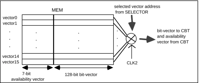
2.5 MEM (Memory) Block
A MEM block has 16 vectors. Each vector in turn is composed of a bit-vector and an availability vector.
A bit-vector has 128 mapping bits. Each mapping bit represents the allocation status of the corresponding cache memory block.
An availability vector has 7 availability bits. It represents the size of the largest contiguous run of free mapping bits in that bit-vector.
. . . .
. .
vector0 vector1
vector14 vector15
. . .
. . .
CLK2
Selected Vector Address from SELECTOR
Bit-vector to CBT and Availability-vector from CBT
MEM
availabilitys vector
bit-vector
The CBT determines which mapping bits in bit-vector should be allocated or freed by considering:
. current status of the mapping bits
. in allocation or deallocation mode
. B value
. Brounded_up value . starting address of the block to be deallocated
There are 128 flip bits on the flip bus. Each bit is
corresponding to the mapping bit on the same address. If CBT wants to allocate or deallocate a
mapping bit, it will set the corresponding flip bit to '1'. The other flip bit are all '0'.
The CBT will calculate the availability of the new mapping bits in bit-vector and output it through availability bus
The MEM outputs the 128 mapping bits of the bit-vector through IN bus.The bit-vector is specified by the selected vector address (SEL) sent from SELECTOR.
At the rising edge of CLK2, the MEM will toggle the value of mapping bits that have the corresponding flip bits being set to '1'.
After the toggling, the new mapping bits are sent through IN bus to CBT.
At the falling edge of CLK2, the MEM will update the availability value into the availability vector.
1
2
3
4
5 1
2
3
4
IN
FLIP
IN
AVAIL
CBT MEM
B
Brounded_up
Starting address of block being freed
SEL
CLK2
2.6 2-1 MUX The 2-1 MUX is a 2-to-1 multiplex-er.
During allocation operation,
ALLOC ='1'. The 2–1 MUX will select and output the SELECTOR's data onto the SEL
4-16 DECODER
SELECTOR
2-1 MUX MEM
ALLOC
SEL bus
bus which will select a suitable bit-vector for allocation.
In deallocation operation, the user will specify the block size and the starting address of the memory block. The starting address will go through the LATCH_C and come to the 4–1 DECODER. During deallocation
operation, ALLOC = '0' and the 2–1 MUX will select the starting address from the 4–16DECODER and output it to select the bit-vector.
2.7 4-16 DECODER
This 4-to-16 decoder converts from a 4-bit address to 16 bits of selection information. The 16-bit value will go through the 2–1MUX to MEM and select the desired bit-vector for deallocation operation.
2.8 16-4 ENCODER
This 16-to-4 encoder converts from 16 bits of selection information to a 4-bit address. During allocation operation, the address of selected bit-vectors generated from SELECTOR will go through the 2–1MUX and 16–4 ENCODER and is finally output to the user.
2.9 ERROR
ERROR will be set to '0' only when an “error” occurs. In allocation operation, possible errors are:
• User requests an allocated block size that is larger than 128 ( number of all mapping bits on a bit-vector ).
• SELECTOR cannot find any bit-vector with possible possible ABRS (allocation block of the requested size).
In deallocation operation, a possible error is:
3. System Data Flow
The memory allocator can allocate or deallocate an arbitrary number of requested blocks (mapping bits) in a single clock cycle. How can it allocate or free the mapping bits? We now illustrate the operations through the data flow diagrams.
3.1 Allocation operation 3.1.1 Functional timing
The input data, ALLOC and B[7:0], must be valid before the rising edge of CLK1. ADDR_OUT[10:0] (starting address of allocated block) and ERROR will be latched at the rising edge of CLK2. The timing for sequential allocation operations is:
CLK1
CLK2
ALLOC
B[7:0]
ADDR_OUT[10:0]
ERROR
cycle 1 cycle 2
allocation allocation
D 1
D 1 D 2
D 1 D 2
D 2 D 3
3.1.2 Data Flow
LATCH_C LATCH_A
ROUND_UP
COMPARATOR
MEM CBT
21MUX
164ENCODER
LATCH_D LATCH_E
ERROR
AV0 AV1
AV14 AV15
IN
FLIP
AVAIL
OUT_ADDR
ADDR_OUT
ERROR
B ALLOC
. . . .
3
4
5
6 7
1
2 1
6
7 7
8 9
B
Brounded_up
The data flow sequence is listed below: After rising edge of CLK1
step 1. Triggered by the rising edge of CLK1, the B[7:0] (requested
allocation-block size) and the ALLOC (operation mode) are latched in through the LATCH_A and the LATCH_C.
step 2. The B[7:0] value is rounded_up for availability comparision and CBT processing.
step 4. The selected vector address is sent out through the 2–1MUX and finally to the MEM.
step 5. The bit-vector selected by selected vector address is sent to the CBT through the IN bus.
step 6. The CBT calculates the location of the requested allocated block from the information of B[7:0] , Brounded_up[7:0] , and IN[127:0]. It then sets the corresponding flip bit to '1'. The 128 flip bits are sent out through FLIP[127:0].
At the same time, the starting address of the allocated block is generated and passed out to the LATCH_D.
After rising edge of CLK2
step 7 . Triggered by the rising edge of CLK2, the MEM uses the flip-bit value to update the corresponding vector. The updated bit-vector is sent out to the CBT.
At the same time, the starting address and error signal are latched out through LATCH_D and LATCH_E.
step 8 . The CBT generates the availability value of the updated bit-vector and send it to the MEM through AVAIL[7:0].
After falling edge of CLK2
3.2 Deallocation operation 3.2.1 Functional timing
Timing for sequential free operations:
CLK1
CLK2
ALLOC
B[7:0]
ADDR_OUT[10:0]
ERROR
cycle 1 cycle 2
D 1
D 1 D 2
D 2 D 3
not valid not valid
D 0
free free
D 1 D 2
D 0 ADDR_IN[10:0] not valid
3.2.2 Data Flow
LATCH_C LATCH_A
ROUND_UP
MEM CBT
21MUX LATCH_E
ERROR
IN
FLIP
AVAIL
ERROR
B ALLOC
3
5 1
2 1
4
5
6
B
Brounded_up 416DECODER
LATCH_B
1
2
7
ADDR_IN
The data flow sequence is listed below: After rising edge of CLK1
step 1. Triggered by the rising edge of CLK1, B[7:0] (requested allocated block size), ADDR_IN[10:0] (starting address of the block being freed), and ALLOC (operatIon mode) are latched in through LATCH_A, LATCH_B, and LATCH_C.
step 2. The B[7:0] value is rounded_up for CBT processing.
4–16 ENCODER converts the ADDR_IN[10:7] to the selected vector address.
step 3. The bit-vector selected by selected vector address is sent to the CBT through the IN bus.
After rising edge of CLK2
step 5. Triggered by the rising edge of CLK2, the MEM uses the flip bits value to update the corresponding vector. The updated bit-vector is sent out to the CBT.
step 6. The CBT generates the availability value of the updated bit-vector and sends it to the MEM through AVAIL[7:0].
After falling edge of CLK2
4. Circuit Description 4.1 CBT
The MEM connects the selected bit-vector and availability vector to the CBT. This connection is controlled by the selecting address from SELECTOR in allocation mode or from the user in deallocation mode. The CBT will perform the following operations in the various modes:
a. Allocation mode:
The CBT enters allocation mode when ALLOC pin = '1'. step 1. Receives the requeated block size B from LATCH_A.
Receives the rounded_up size Broundup, from ROUND_UP. This is equal to the size of the ABRS (allocation block of the requested size).
Receives the selected bit-vector from MEM. step 2. Finds out the first available ABRS.
step 3. Generates the starting address of the first available ABRS. Finds out the position of the mapping bits intended to be allocated. Sets the corresponding flip bits to '1'.
step 4. Generates the availability value when it receive the new bit-vector from the MEM.
b. Deallocation mode:
The CBT enters deallocation mode when ALLOC pin = '0'. step 1. Receives the requeated block size B from LATCH_A.
Receives the starting address of the deallocating block from user through LATCH_B.
step 2. Finds out the position of the mapping bits intended to be freed. Sets the corresponding flip bits to '1'.
step 3. Generates the availability value when it receives the new bit-vector from the MEM.
How can the CBT perform the above functions? We will illustrate the operation by looking at the mechanisms for:
• generating the availability vector • generating the flip-bit signal • finding the first available ABRS • generating the starting address
4.1.1 Generation of availability value
Let's look at an example of a CBT for an 8-bit bit-vector. Fig 4.1
8
4
2
1 Size
: two input OR fate for detecting contiguous '0'
: low active pull-low wire-OR point Availability
1 0 1 1 0 0 0 0
1 1 0 0
1 0
1
0 0 1
0 AV0
AV1 AV2 AV3
Node level
3
2
1
0
The AV[3:0] are the availability lines of this CBT. Each AV line is connected to a pull-high resistor and is pulled down to '0' whenever one or more connecting node-to-node lines (the horizontal lines in the diagram) are '0' (low-active pull-low wired-OR). Any '0' on the node-to-node line will pull the same-level AV line to '0'. If no '0' exists, the AV line on the same level will remain '1'. In this example, AV0=AV1=AV2='0'. This means that contiguous runs bits of length 20, 21, and 22 exist. The system can know how many contiguous free mapping bits are present by checking the availability value at any time.
4.1.2 Find the first available ABRS (allocation block of the requested size) How to calculate the size of ABRS?
size of ABRS = 2 log B
In the or-tree, if the output of an level-n or-gate is '0', the children below this or-gate must all be '0'. Therefore, if size of ABRS is 2n, the CBT will look on level n to search for the first or-gate with a '0' output value.
Fig 4.2
: two input AND gate 1 0 1 1 0 0 0 0
Node level
3
2
1
0
a
b c
d e f g
0 1 0 0
0 0
0 Searching path
Let's look at the possible input/output relations in an and-gate: Fig 4.3
: two input AND gate
a: b: c:
0 1 1 0 0 0
0 0
0
L R L R L R
Whenever there is at least one '0' on the input pins, the output will be '0'. Therefore, if we look down from the top of and-gate and see a '0', we can be sure that there is at least one '0' among its children. As we are only
concerned with the side the first '0' is located on, we can derive a simple relationship from the above three and-gates.
• When the left input pin is '1', the first '0' must be on the left. • When the left input pin is '0', the first '0' must be on the right.
and-node a. Whenever the search path comes to an and-node, it will check the value on the left input pin. A value of '1' means that the first '0' must be on the right, so the search path will proceed down to the right child. A value of '0' means the first '0' must be on the left, so the search path will go down to the left child.
In this example, the search path will go down in this way: Fig 4.4
: two input AND gate 1 0 1 1 0 0 0 0
a
b c
d e f g
0 1 0 0
0 0
0 Searching path
node
value of left input pin
turning direction
a
b
d
0
0
1
left
right left
a0 a1 a2 a3 a4 a5 a6 a7
It finally reaches the first '0' at a1.
In this example, we are searching for the first '0' on level 0. We can select the first '0' on a higher level by dynamically ignoring the and-nodes below that level.
The or-tree can show us if a block of 2n contiguous '0's exists or not. The and-tree leads us to find the first '0' on a particular level. We can combine these two functions to find the first ABRS.
Fig 4.5
1 0 1 1 0 0 0 0
1 1 0 0
1 0
1
a0 a1 a2 a3 a4 a5 a6 a7
a
b c
d e f g
0 1 0 0
0 0
0 Searching path
1
1 0 1 1 0 0 0 0
a : AND-gate ( AND-node )
: OR-gate ( OR-node )
: connection point
Therefore, if we have to find the first '0' on level 0, we can connect all the level-0 pins to the and-tree as in the diagram above. The search path will go down through each and-node and finally locate the first ABRS at address a1.
Assume we have to allocate three blocks. We need to find the first ABRS of size 22. Therefore we search the first '0' on level 2.
Fig 4.6
1 0 1 1 0 0 0 0
1 1 0 0
1 0
1
a0 a1 a2 a3 a4 a5 a6 a7
a
0 Searching path
a : AND-gate ( AND-node )
: OR-gate ( OR-node )
: connection point Level
3
2
1
0
The and-tree can easily see that the first '0' is located on the right. This means the first ABRS is on the right side of the and-tree.
The connection between the and-tree and the or-tree is set up dynamically based on the ABRS size. The connection diagram is shown below:
Fig 4.7
a0 a1 a2 a3 a4 a5 a6 a7
a
b c
d e f g
a : AND-gate ( AND-node )
: OR-gate ( OR-node )
: connection point sw 1b
sw2b sw3b sw3a
sw2a
sw1a
s1 s2
s3
: high-active array switch
: low-active array switch
The ABRS size, held in s3s2s1s0, is used to control the ON/OFF of the array switches. (s0 is not shown in the diagram because there are no child nodes below it.) For example, if size = 22 = 01002.
a3 = 0 sw3a = OFF sw3b = ON
a2 = 1 sw2a = ON sw2b = OFF
a1 = 0 sw1a = OFF sw1b = ON
a0 = 0 nil nil
The connection will then be as shown in Fig 3.6.
How can the CBT locates the position of the bits allocated and set the corresponding flip-bit to '1'?
Assume we have a flipper-tree which works together with the and-tree. The direction data (value of the left input pin of each and-node) for searching is passed to the flipper-nodes.
Fig 4.8
: AND node
: FLIPPER node Enable path
In the flipper-tree, we have an enable path going down from the top. It is similar to the search path in the and-tree. The enable path can find the first ABRS, which is equivalent to the first '0' at the corresponding level, by checking the direction data from the and-tree.
From the and-tree diagram Fig 4.4, the direction data from each and-node is used by the flipper-node in the corresponding location in the figure below. By the same mechanism, the enable path can easily find the first '0'. Assume we use the value of the left output pin on each and-node in diagram Fig 3.5 and put them into the flipper-tree:
0
0 0
1 1 0 0
a0 a1 a2 a3 a4 a5 a6 a7 Enable path
When the direction data from the and-node is '0', the enable path goes down to the left by setting the left output pin to '1'. If it is '1', enable path descends to the right by setting the right output pin to '1'. Finally, a continuous enable path forms going from top to the first '0' at address a1.
How can the flipper-tree generate the flip-bit signal? The enable path is formed by setting to '1' all the lines it passes. The lines being set to '1' are activated. The other lines are all '0'; they are not activated. The enable path has the useful characteristic that it always points to the first ABRS. If we want to allocate 2n blocks (flip 2n mapping bits), we can send a signal to the level-n
flipper-node at which the enable path is pointing. This signal is called the flip control and the flipper-node that receives a flip control will propagate a flip signal down to the lowest-level bits. Here, we use a new line, called the flip line, to propagate the flipping signal downward. Looking from the site of a flipper-node, the flip line coming from the parent is called flip input, while the flip lines going to the children are called flip outputs.
Fig 4.10
FLIPPER NODE
flip input enable input
flip output
enable output
enable output flip
output flip contol
A flip line is activated by being set to '1' and deactivated by being set to '0'. For example, in case of allocated block size = 2 = 21, we can set the flip control of level-1 nodes to '1'. This will cause the flip output of level-1 nodes to be '1' if the flip output is going out with the enable path. The flip output signal will be propagated down and eventually used as the flip-bit signal for an allocation or deallocation operation. In this example, all four flipper-nodes on level-1 receive the same flip control value. However, the flip outputs are set
according to the following conditions: if the flip input of a flipper-node ='1'
set the flip outputs to both left and right children to '1' … (Cond. 1) if the flip input of a flipper-node ='0'
{
if the flip control = '1' {
if the left eable output = '1'
set the left flip output to '1' … (Cond. 2 ) if the right enable output = '1'
set the right flip output to '1' … (Cond. 3 ) }
}
In all other conditions, the flip outputs are kept '0' … (Cond. 4 )
If the allocated block size = 4 = 22 and the enable line is pointing down to a0, the flipper-tree will look like this:
Fig 4.11
1
0
0
: active Enable line ( forms Enable path ) : inactive Enable line
: active Flip line
: inactive Flip line
* When the Enable or Flip line is active, it = '1'.Else, it = '0'. Flip control
Level
2
1
0
a
b c
The left flip input of node a is set '1' because of condition 2. The flip outputs of node a, d, and e are all set to '1' because of condition 1. The flip control for each level l is actually the value of bit l of the requested block size. A
requested block size of 4 (100 in binary) will set the flip control on level-2 nodes to '1' while size of 6 (110 in binary) will set the flip control on all level-2 and level-1 nodes to '1'.
How can we allocate blocks of a size that is not exactly equal to 2k?
We do this by adding another feature to the enable line. From Fig 4.9, we know that direction data from and-tree will direct the enable line to propagate down to the left child or to the right child. We call this data “address
control.” With the address-control signal, the flip-node becomes: Fig 4.12
FLIPPER NODE
flip input enable input
flip output
enable output
enable output flip
output flip contol
to left child to right child
address control
( from AND-tree)
In the diagram Fig 4.9, we have: if the enable input = '1'
if the address control = '1'
set right enable output to '1' else
set left enable output to '1' We now change these conditions to:
if the enable input = '1' {
if the flip control = '0' {
if the address control = '1'
Set right enable output to '1' … (Cond. 5) else
else
Set both right and left enable outputs to '1' … (Cond. 7) However, the right flip output will be kept '0' (Cond. 3 does not hold)
} else
All the enable outputs are kept '0'
Suppose the allocated block size = 5, then the flip control = 5 (101 in binary). Assume we have a bit-vector of value 00000000 in binary.
Fig 4.13
1
0
: active enable line ( forms enable path ) : inactive enable line
: active flip line
: inactive flip line flip control
Level
2
1
0
a
b c
d e f g
1
a0 a1 a2 a3 a4 a5 a6 a7 1 1 1 1 1 0 0 0
Thus, the flip outputs on a0to a4 are set to '1'. Here different nodes follow different conditions.
conditions for conditions for node enable line flip line
a Cond. 7 Cond. 2
b Cond. 6 Cond. 1
c Cond. 6 Cond. 4
d Cond. 6 Cond. 1
e Cond. 8 Cond. 1
f Cond. 6 Cond. 2
g Cond. 8 Cond. 4
, and-node, and other auxillary logic to form a CBT cell (cbt_c), which is a basic unit of the CBT block. The logic of the CBT cell is shown in Fig. C3 (on page 61). In Fig. 4.13, the enable outputs on the level-0 flipper-node are not used because they are the lowest-level nodes. In Fig. C4 (page 62) is shown a simplified version of a flip node called a ground-level flip cell (gflip_c), which does not have the enable output pins. Similary, in the CBT cell, the switching circuits between or-nodes and and-nodes are not necessary on level 0, and are therefore omitted. This yields a simplified version called a ground-level CBT cell (gcbt_c). The logic of gcbt_c is shown in Fig. C5 (page 63).
The cbt_c and gcbt_c are the basic units of the complete binary tree (CBT). Each cell contains an or-node, an and-node, and a flipper-node. The cells can be easily used to construct a CBT of various sizes. In our application, we build a CBT with 128 flip bits (128 flip outputs from the lowest-level nodes).
The whole circuit is shown in Fig. C6 (page 64). The lowest level is composed of four 32-bit CBTs. The logic for a 32-bit CBT is shown in Fig. C7 (page 65). How can one generate the starting address of the allocated blocks?
The enable path has a useful characteristic that it always goes down and
reaches the starting bit of allocated block when it arrives the lowest level. We can easily extract the address from the enable path by wired-oring the left enable output pin of every flipper-node. As there are no enable outputs on the level-0 flipper-node, we can wired-or the left flip output pins and this will give us the same result.
For example, if the enable path goes down to address a4and two bits are allocated, the flipper-tree will look like this:
: active Enable line ( forms Enable path ) : inactive Enable line
: active Flip line
: inactive Flip line
a
b c
d e f g
a0 a1 a2 a3 a4 a5 a6 a7 0 0 0 0 1 1 0 0
1
0
0
Starting address
OUT_ADDR 2
OUT_ADDR 1
OUT_ADDR 0
: high-active pull-low wire_OR
All the OUT_ADDR lines are connected to the pulled-high resistor.
Whenever the enable path goes to the left, it will pull the OUT_ADDR line to '0'. If it goes down to right, the OUT_ADDR will remain '1'. In this example, the address generated is 100, which is the address of a4.
Deallocation operation:
In the CBT, a free operation is similar to an allocation operation except that the location of block being freed is specified externally by the user. In this case, the address control for flipper-node is supplied by the user, not from the and-node. In both the CBT cell and ground-level CBT cell, we have a
selecting pin (SELECT) to choose the address from either the internal and-node or the external ADDR_IN signal. In allocation operation, the SELECT pin is set to '1'. Otherwise, it is set to '0'.
4.2. Other blocks 4.2.1 MEM
The MEM is composed of 8 vectors. Each vector in turn is composed of a 7-bit availability vector and a 128-bit bit-vector. The vector is selected by the vector address from SELECTOR and its bit-vector is output to the CBT for
will be loaded into the availability vector in the same MEM vector from which it was obtained.
Fig 5.1
. . . .
. .
vector0 vector1
vector14 vector15
. . .
. . .
CLK2
selected vector address from SELECTOR
bit-vector to CBT and availability vector from CBT
MEM
7-bit availability vector
128-bit bit-vector
The logic of MEM is shown in Fig C8 (page 66). The MEM is separated into two parts, the toggle-memory (tmem) and the D-memory (dmem). The toggle-memory contains eight 128-bit bit-vectors and is shown in Fig C9 (page 67). The D-memory consists of eight 7-bit availability vectors and is shown in Fig. C10 (page 68). There is a CLR pin to initialize the vectors when the system is started. In our application, two memory blocks are used together to supply 16 vectors for the whole system.
4.2.2 SELECTOR
The SELECTOR compares the rounded_up requested block size
The SELECTOR chooses one of the 16 bit-vectors by the following algorithm: if there are availability-vectors that have exactly the same values as the Brounded_up
{
if the number of such availability-vectors is more than one Choose the one with the lowest address.
else
Select that vector. }
else if there are availability vectors with values larger than Brounded_up
{
if the number of such availability-vectors is more than one Choose the one with the lowest address. else
Select that vector. }
else
Report error.
Each SELECTOR is composed of eight comparators (comp_c) to compare the availability value and one priority selector (priority_sel) to select the right vector address.
Comparator (comp_c): This is an 8-bit comparator. Here, we use a 4-bit comparator to illustrate the concept.
If the rounded_up requested Size = 4 (0100 in binary). We want to have a equal (EQ) bit and greater-than-or-equal (GE) bit to indicate whether the availability-vector value is =, or ≥ the rounded-up request size.
rounded_up availability expected expected requested size vector value EQ value GE value
0100 0000 0 0
0100 0001 0 0
0100 0011 0 0
0100 0111 1 1
0100 1111 0 1
For GE :
A[3:0] B[3:0] Ci = Ai * Bi GE=C0+C1+C2+C3
0100 0000 0000 0
0100 0001 0000 0
0100 0011 0000 0
0100 0111 0100 1
0100 1111 0100 1
where * is and operator + is or operator
For all possible values of B, only the last two B value can have the GE set to '1'. Therefore, GE can be obtained by first performing Ci = (Ai * Bi) followed by oring all the C bits together.
For EQ :
A[3:0] B[3:0] Ci = Ai * Bi D[3:0] EQ = D0+D1+D2+D3
0100 0000 0000 0000 0
0100 0001 0000 0000 0
0100 0011 0000 0000 0
0100 0111 0100 0100 1
0100 1111 0100 0000 0
where * is and operator D0 = C0*(~B1) + is or operator D1 = C1*(~B2)
D2 = C2*(~B3) D3 = C3*1
cascading two 8-vector SELECTORs to form a 16-vector SELECTOR. The SELECTOR with the higher priority on its vector address will connect the CASCADE_IN pin to '0'. The one with lower priority will connect the CASCADE_IN pin to '1'. A diagram of connecting two SELECTORs and the MEM blocks is shown below: GEIN, GEOUT below
AV0 AV1
AV6 AV7
AV8 AV9
AV14
AV15 . . . . . . EQIN
EQOUT GEIN
GEOUT CASCADE_IN
EQIN
EQOUT GEIN GEOUT
ERROR
ERROR
CASCADE_IN
NOR
MEM
MEM rounded_up
requested block size
Error
SELECTOR and MEM blocks for vector[7:0]
SELECTOR and MEM blocks for vector[15:8]
4.2.3 ROUND_UP
ROUND_UP converts the requested block size B to the rounded_up block size Brounded_up according to the following relation:
Brounded_up = 2 log B
The maximum requested block size in our system is 128. ROUND_UP will set ERROR to '0' if B is larger than 128. If B is exactly equal to 128,
ROUND_UP will issue a FLIP_ALL signal to the CBT to allocate all 128 mapping bits in a faster way. The circuits for ROUND_UP is shown on Fig C14 (page 72).
4.2.4 2-1 MUX
pin (ALLOC). 2–1MUX will output the vector address from the sourse to the MEM.
If ALLOC = '1' source is the SELECTOR
else source is the external ADDR_IN. The circuits are shown on Fig C15 (page 73).
4.2.5 16-4 ENCODER
A 16-to-4 encoder converts vector converts 16 address lines to a 4-bit ADDR_OUT[10:7]. The circuit is shown in Fig. C16 (page 74).
4.2.6 4-16 DECODER
A 4-to-16 decoder converts a 4-bit ADDR_IN[10:7] to 16 bits for internal processing. The circuit is shown on Fig C17 (page 75).
4.2.7 LATCHES
The are five latches in this system. They are all triggered by the positive edge of a clock and cleared by CLR. The input latches are all triggered by CLK1 while output latches are triggered by CLK2. The logic of LATCH_C is shown on Fig C18 (page 76) as an example.
These signals are latched in or out:
L a t c h Signals
LATCH_A B[7:0] (the size of the requested allocation block size or the block to be freed)
LATCH_B ADDR_IN[10:0] (starting address of block to be freed)
LATCH_C ALLOC (operation mode)
LATCH_D ADDR_OUT[10:0] (starting address of block that is allocated)
LATCH_E ERROR (error signal )
Three simulation patterns are used to debug the circuits and measure the timing characteristics during the final development stage. In this section, several items will be discussed:
. the functional timing.
. the gate delay and the simulation pins.
. three test patterns and the simulation waveforms. . the AC timing.
5.1 FUNCTIONAL TIMING
The system can allocate or free a block of arbitrary size in a single clock cycle. Five different combinations of operation timings are described below:
5.1.1 Allocation/allocation cycles
The timing for sequential allocation operations:
CLK1
CLK2
ALLOC
B[7:0]
ADDR_OUT[10:0]
ERROR
cycle 1 cycle 2
allocation allocation
D 1
D 1 D 2
D 1 D 2
D 2 D 3
D 0 D 0
5.1.2 Deallocation/deallocation cycles
The timing for sequential deallocation operations:
CLK1
CLK2
ALLOC
B[7:0]
ADDR_OUT[10:0]
ERROR
cycle 1 cycle 2
D 1
D 1 D 2
D 2 D 3
not valid not valid
D 0
deallocation
D 1 D 2
D 0 ADDR_IN[10:0] not valid
deallocation
For correct operation, the ALLOC and B[7:0] must be valid before the rising edge of CLK1.
5.1.3 Allocation/deallocation/allocation cycles
CLK1
CLK2
ALLOC
B[7:0]
ADDR_OUT[10:0]
cycle 1 cycle 2
D 1 D 2
D 1 not valid
D 0
allocation deallocation
D3
allocation cycle 3
D 3
D 2
ERROR D 0 D 1 D 2 D 3
not valid not valid not valid
ADDR_IN[10:0]
5.1.4 Allocation/nop/allocation cycles
A cycle is a “nop” when no operation is done. When the requested block size B[7:0] (in either allocation or deallocation operation) is zero, the system will assume the user is not using the memory allocator and will enter nop mode. The ERROR pin remains '0' during this cycle.
CLK1
CLK2
ALLOC
B[7:0]
ADDR_OUT[10:0]
ERROR
cycle 1 cycle 2
D 1
D 1 ZERO
D 0
D 1 not valid
D 0
allocation nop
D3
allocation cycle 3
D 3
D 3 not valid
ZERO
5.1.5 Deallocation/nop/deallocation cycles
CLK1
CLK2
ALLOC
B[7:0]
ADDR_OUT[10:0]
cycle 1 cycle 2
D 1
D 1 ZERO
not valid
deallocation nop
D3 cycle 3
D 3 not valid
not valid not valid
ERROR D 0 D 1 ZERO D 3
ADDR_IN[10:0]
D 0
not valid not valid
deallocation
5.2.1 Gate Delay
In the simulation, we use the following delay time for different logic gates.
Gate Type
TPLH, TPHL TPLZ, TPHZ, TPZL, TPZH
CLKtoQ0, CLKtoQ1, CLKtoQN0, CLKtoQN1
NOT 0.5 ns — —
BUF 1.0 ns — —
TRIBUF 1.2 ns 1.2 ns —
NAND 2 inputs 3 inputs 4 inputs
0.8 ns 0.8 ns 1.0 ns
— — —
— — — NOR 2 inputs
3 inputs 4 inputs
0.8 ns 0.8 ns 1.0 ns
— — —
— — — AND 2 inputs
3 inputs 4 inputs
0.8 ns 0.8 ns 1.0 ns
— — —
— — — OR 2 inputs
3 inputs 4 inputs
0.8 ns 0.8 ns 1.0 ns
— — —
— — —
LATCH — — 7.5 ns
T_F/F — — 3.5 ns
D_F/F — — 7.5 ns
5.2.2 Simulation pins External pins:
N a m e Input/output Functions
CLK1 input Clock 1
CLK2 input Clock 2
CLR input Clear pin. This is the signal for initializaton
B[7:0] input Requested block size (allocation or deallocation operation)
ALLOC input Operation mode
ADDR_IN[10:0] input Starting address of the requested freeing block
ADDR_OUT[10:0] output Starting address of the allocated block
Internal pins:
IN[127:0] The bit-vector outputed from the MEM to the CBT.
FLIP[127:0] The flip control bits output from the CBT to MEM
PRE[7:0] The pre_roundup value of the requested block size.
POST[7:0] The post_roundup value of the requested block size.
FLIP_ALL When user alocates 128 mapping bits, FLIP_ALL will be '1'
ALLOC_ The ALLOC signal after being latched in.
SE0[15:0] The selected vector address outputed from the SELECTOR.
DEO[15:0] The output pf 4-16 DECODER.
ERROR_ The error signal before being latched out.
AVAIL[7:0] The availability value of circuit processing Bit-vector. It is generatd from CBT.
SEL[15:0] The selected vector address going into the MEM.
AV[15:0] The availability vector values of vector[15:0].
OUT_ADDR[6:0] The ADDR_OUT signal before latched out.
5.3 TEST PATTERNS AND SIMULATION WAVEFORMS
Three different test patterns are used for allocation, deallocation, and mixed operations.
5.3.1 Allocation test a. Test patterns:
oper- ADDR_ availa- ADDR_
ation IN B <---current bit-vector ---> bility OUT
reset alloc alloc alloc alloc alloc alloc alloc alloc alloc alloc alloc alloc alloc alloc alloc alloc alloc alloc alloc alloc alloc alloc alloc alloc alloc alloc alloc alloc alloc alloc alloc alloc alloc alloc alloc free alloc reset 1 2 3 4 5 6 7 8 9 10 15 20 13 1 2 3 4 5 6 65 65 65 65 128 65 65 65 65 128 65 65 128 65 5 3 13 7 reset 0 0 0 0 0 0 0 0 0 0 0 0 1 0 0 0 0 0 1 2 3 4 5 6 7 8 9 10 11 12 13 14 15 1 0 0 0 0000 0000 0000 0000 0000 0000 0000 0000 0000 0000 0000 0000 000F 0000 000F 000F 000F 000F 1F0F 0000 0000 0000 0000 0000 FFFF 0000 0000 0000 0000 FFFF 0000 0000 FFFF 0000 0000 1F7F 1F7F 1F7F 0000 0000 0000 0000 0000 0000 0000 0000 0000 0000 0000 0000 FFFF 0000 FFFF FFFF FFFF FFFF FFFF 0000 0000 0000 0000 0000 FFFF 0000 0000 0000 0000F FFF 0000 0000 FFFF 0000 0000 FFFF E000 E07F 0000 0000 0000 0000 0000 0000 0000 0000 0000 0000 0000 7FFF 7FFF 0000 7FFF 7FFF 7FFF 7FFF 7FFF 0000 0000 0000 0000 0000 FFFF 0000 0000 0000 0000 FFFF 0000 0000 FFFF 0000 0000 7FFF 7FFF 7FFF 0000 0000 0000 0000 0000 0000 0000 0000 0000 0000 03FF 03FF 03FF 0000 03FF 03FF 03FF F3FF F3FF 0000 0001 0001 0001 0001 FFFF 0001 0001 0001 0001 FFFF 0001 0001 FFFF 0001 0000 F3FF F3FF F3FF 0000 0000 0000 0000 0000 0000 0000 0000 0000 01FF 01FF 01FF 01FF 0000 01FF 01FF 71FF 71FF 71FF 0000 FFFF FFFF FFFF FFFF FFFF FFFF FFFF FFFF FFFF FFFF FFFF FFFF FFFF FFFF 0000 71FF 71FF 71FF 0000 0000 0000 0000 0000 0000 0000 007F FF7F FF7F FF7F FF7F FF7F 0000 FF7F FF7F FF7F FF7F FF7F 0000 FFFF FFFF FFFF FFFF FFFF FFFF FFFF FFFF FFFF FFFF FFFF FFFF FFFF FFFF 0000 FF7F FF7F FF7F 0000 0000 0000 0000 0000 001F 3F1F 3F1F 3F1F 3F1F 3F1F 3F1F 3F1F 0000 3F1F 3F1F 3F1F 3F1F 3F1F 003F FFFF FFFF FFFF FFFF FFFF FFFF FFFF FFFF FFFF FFFF FFFF FFFF FFFF FFFF 1F3F 3F1F 3F1F 3F1F 0000 0001 000D 007D 0F7D 0F7D 0F7D 0F7D 0F7D 0F7D 0F7D 0F7D 0F7D 1FFF 0F7D 3F7F 3F7F 3F7F 3F7F 1FFF FFFF FFFF FFFF FFFF FFFF FFFF FFFF FFFF FFFF FFFF FFFF FFFF FFFF FFFF 1FFF 3F7F 3F7F 3F7F FF 7F 7F 7F 7F 7F 7F 7F 7F 7F 3F 3F 0F 7F 0F 0F 0F 0F 0F 7F 3F 3F 3F 3F 00 3F 3F 3F 3F 00 3F 3F 00 3F 7F 03 0F 07 -— 000 002 004 008 010 018 020 028 030 040 050 060 080 001 00C 03C 04C 078 090 100 180 200 280 300 380 400 480 500 580 600 680 700 780 98 74 UNVALID 60
b. Simulation waveforms:
5.3.2 Deallocation test a. Test patterns:
oper- ADDR_ vector availa- ADDR_ ation IN B # <---current bit-vector ---> bility OUT
reset alloc alloc alloc alloc alloc alloc alloc alloc alloc alloc alloc alloc alloc alloc alloc alloc free free free free free free free free free free free free free free free free free free free free free free free reset — — — — — — — — — — — — — — — — 4 2 10 30 40 58 68 7A 1D0 A2 108 210 3A0 2C0 404 308 490 7A0 560 760 5F0 681 603 reset 128 128 128 128 128 128 128 128 128 128 128 128 128 128 128 128 3 1 5 7 21 4 8 2 15 2 7 15 29 31 3 7 11 10 30 8 15 1 1 reset 0 1 2 3 4 5 6 7 8 9 10 11 12 13 14 15 0 0 0 0 0 0 0 0 3 1 2 4 7 5 8 6 9 15 10 14 11 13 12 0000 FFFF FFFF FFFF FFFF FFFF FFFF FFFF FFFF FFFF FFFF FFFF FFFF FFFF FFFF FFFF FFFF FFFF FFFF FFFF FFFF FFFF FFFF FFFF F3FF FFFF FFFF FFFF FFFF FFFF FFFF FFFF FFFF FFFF FFFF FFFF FFFF 8000 FFFF FFFF 0000 FFFF FFFF FFFF FFFF FFFF FFFF FFFF FFFF FFFF FFFF FFFF FFFF FFFF FFFF FFFF FFFF FFFF FFFF FFFF FFFF FFFF FFFF 00FF 00FF FFFF FFFF FFFF FFFF FFFF FFFF FFFF FFFF FFFF FFFF FFFF FF00 FFFF FFFF FFFF 0000 FFFF FFFF FFFF FFFF FFFF FFFF FFFF FFFF FFFF FFFF FFFF FFFF FFFF FFFF FFFF FFFF FFFF FFFF FFFF FFFF FFE0 F0E0 F0E0 F0E0 8000 FFFF FFFF FFFF FFFF 8000 FFFF FFFF FFFF FFFF C000 FFFF FFFF FFFF FFFF 0000 FFFF FFFF FFFF FFFF FFFF FFFF FFFF FFFF FFFF FFFF FFFF FFFF FFFF FFFF FFFF FFFF FFFF FFFF FFFF FFFF 0000 0000 0000 0000 FFFF FFFF FFFF FFFF FFFF 0000 FFFF FFFF FFFF FFFF 0000 FFFF FFFF FFFF FFFF 0000 FFFF FFFF FFFF FFFF FFFF FFFF FFFF FFFF FFFF FFFF FFFF FFFF FFFF FFFF FFFF FFFF FFFF FFFF FFFF FF80 FF80 FF80 FF80 FF80 FFFF FFFF FFFF FFFF E000 FFFF FFFF FFFF FFFF FFFF FFFF FFFF FFFF FFFF FFFF 0000 FFFF FFFF FFFF FFFF FFFF FFFF FFFF FFFF FFFF FFFF FFFF FFFF FFFF FFFF FFFF FFFF FFFF FFFF FFFF FFFF FFFF FFFF FFFF FFFF FFFF FFF3 FFFF FFFF 0000 FFFF FFFF FFFF FFFF FC00 FFFF FFFF FFFF FFFF FFFF 0000 FFFF FFFF FFFF FFFF FFFF FFFF FFFF FFFF FFFF FFFF FFFF FFFF FFFF FFFF FFFF FFFF FFFF FFFF FFE0 FFE0 FFE0 FFE0 FFE0 FFE0 FFFF FFFF FFFF 8000 FFFF FFFF FFFF FFFF F800 FFFF FFFF FFFF FFFF FFFF FFFF 0000 FFFF FFFF FFFF FFFF FFFF FFFF FFFF FFFF FFFF FFFF FFFF FFFF FFFF FFFF FFFF FFFF FF8F FF8B FF8B FF8B FF8B FF8B FF8B FF8B FFFF FFFF 80FF FFFF FFFF FFFF FF8F 80FF FFFF FFFF FFFF FFFF FFFF FFFD FFF7 FF 00 00 00 00 00 00 00 00 00 00 00 00 00 00 00 00 03 03 07 07 1F 1F 1F 1F 0F 03 07 0F 1F 1F 03 07 0F 0F 1F 0F 0F 01 01 N O T V A L I D
b.Simulation waveforms :